Transcription
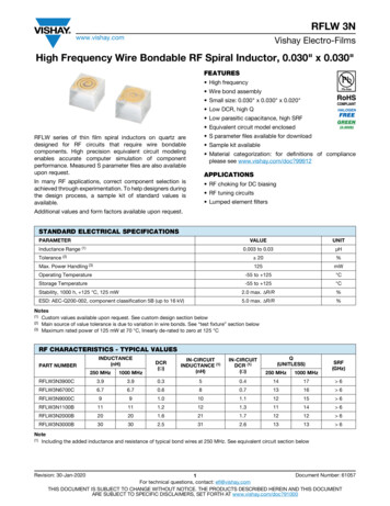
RFLW 3Nwww.vishay.comVishay Electro-FilmsHigh Frequency Wire Bondable RF Spiral Inductor, 0.030" x 0.030"FEATURES High frequency Wire bond assembly Small size: 0.030" x 0.030" x 0.020" Low DCR, high Q Low parasitic capacitance, high SRF Equivalent circuit model enclosedRFLW series of thin film spiral inductors on quartz aredesigned for RF circuits that require wire bondablecomponents. High precision equivalent circuit modelingenables accurate computer simulation of componentperformance. Measured S parameter files are also availableupon request. S parameter files available for downloadIn many RF applications, correct component selection isachieved through experimentation. To help designers duringthe design process, a sample kit of standard values isavailable. RF choking for DC biasing Sample kit available Material categorization: for definitions of complianceplease see www.vishay.com/doc?99912APPLICATIONS RF tuning circuits Lumped element filtersAdditional values and form factors available upon request.STANDARD ELECTRICAL SPECIFICATIONSPARAMETERInductance Range(1)VALUEUNIT0.003 to 0.03μHTolerance (2) 20%Max. Power Handling (3)125mWOperating Temperature-55 to 125 CStorage Temperature-55 to 125 CStability, 1000 h, 125 C, 125 mW2.0 max. R/R%ESD: AEC-Q200-002, component classification 5B (up to 16 kV)5.0 max. R/R%Notes(1) Custom values available upon request. See custom design section below(2) Main source of value tolerance is due to variation in wire bonds. See “test fixture” section below(3) Maximum rated power of 125 mW at 70 C, linearly de-rated to zero at 125 CRF CHARACTERISTICS - TYPICAL VALUESPART NUMBERINDUCTANCE(nH)Q(UNITLESS)DCR( )IN-CIRCUITINDUCTANCE (1)(nH)IN-CIRCUITDCR (1)( )250 MHz1000 MHz50.41417 6SRF(GHz)250 MHz1000 6 6RFLW3N9000C991.0101.11215 6RFLW3N1100B11111.2121.31114 6RFLW3N2000B20201.6211.71212 6RFLW3N3000B30302.5312.61313 6Note(1) Including the added inductance and resistance of typical bond wires at 250 MHz. See equivalent circuit section belowRevision: 30-Jan-2020Document Number: 610571For technical questions, contact: efi@vishay.comTHIS DOCUMENT IS SUBJECT TO CHANGE WITHOUT NOTICE. THE PRODUCTS DESCRIBED HEREIN AND THIS DOCUMENTARE SUBJECT TO SPECIFIC DISCLAIMERS, SET FORTH AT www.vishay.com/doc?91000
RFLW 3Nwww.vishay.comVishay Electro-FilmsDIMENSIONS in inches (millimeters)0.030Ø 0.0040.0300.0010.0130.0040.0010.013LENGTH0.030 (0.75) 0.003WIDTH0.030 (0.75) 0.0030.004THICKNESS0.020 (0.5) 0.001BOND PAD DIAMETER4 (0.1)MECHANICAL SPECIFICATIONSChip substrate materialConductor materialConductor thicknessBond pad diameterQuartzGold5 μm 20 %0.004"ATTACHMENT NOTESRFLW inductors are a robust wirebondable thin film product that requires careful attention to tooling set-up during the wirebonding process. Excessive thermo-mechanical wire bonding forces may result in damaging the underlying quartz substrateand cause wire bond failures.GLOBAL PART NUMBER INFORMATIONGlobal Part Number: RFLW3N2000BMNWSGlobal Part Number Description: RFLW 30 x 30 NO PASS 20 nH 20 % WSRFLWMODELSIZEPASSIVATIONRFLW3 30 x 305 50 x 50N none3N2INDUCTANCE(nH)First 4 digitsare significantfigures ofcapacitance00INDUCTANCEMULTIPLIERCODEC 0.001B 0.01A 0.10BTOLERANCECODEM 20 %L 25 %MNSPECIALN noneWSPACKAGINGCODEWAFFLEWS 100 min., 1 mult.EQUIVALENT CIRCUITThe inductor’s spiral trace presents a substantial amount of series resistance, and the close spacing of spiral turns presentmeasurable amounts of stray capacitance that interact with the inductive characteristics.For accurate modeling of the RFLW component in-circuit performance, measured S parameter files are available upon request.Another useful tool commonly used to model the behavior of electronic components at high frequency is the equivalent circuitmodel. While the equivalent circuit model accurately predicts the reactive part of the total impedance, it fails to determine thereal part of the response at high frequency. This is due to the fact that the model does not include skin and proximity effectsthat significantly increase the real part of the impedance as the frequency rises.Revision: 30-Jan-2020Document Number: 610572For technical questions, contact: efi@vishay.comTHIS DOCUMENT IS SUBJECT TO CHANGE WITHOUT NOTICE. THE PRODUCTS DESCRIBED HEREIN AND THIS DOCUMENTARE SUBJECT TO SPECIFIC DISCLAIMERS, SET FORTH AT www.vishay.com/doc?91000
RFLW 3Nwww.vishay.comVishay Electro-FilmsBond WireRbwSpiral InductorLbwLL: Desire inductanceR: Parasitic self resistanceC: Parasitic shunt capacitanceRbw: Bond wire self resistanceLbw: Parasitic bond wire inductanceRCEquivalent Circuit ModelThe equivalent circuit values are presented in the table below:EQUIVALENT CIRCUIT MODEL - TYPICAL VALUESINDUCTANCE(nH)L3.96.79112030SHUNT CAPACITANCE(fF)C11151011DCR( ) (1)0.30.61.01.21.62.5Lbw(nH)Rbw (2)( ) DCR tolerance 20 %(2) Typical bond wires are approximated as being 1.25 mil in diameter gold, totaling a length of 3 mil. The resistance listed above includes theadded effect of the bond wire adhesion to the circuit board and componentTEST FIXTUREThe results presented in the datasheet were obtained by assembling the components onto a thin film test fixture usingnon-conducting epoxy and 1.25 mil diameter gold bond wires.Measurements were conducted using an HP 8753E network analyzer with cascade micro-tech air coplanar probes.The parasitic elements of the bond wires are a major contributor to the tolerance of the lower value components. We considerthe following bond-wire geometry to be typical for the assembly of the RFLW pars:Side pad on inductorCenter pad on inductor20 milAu bond wire pads,20 mil2RFLW20 milAlumina Test Board, 25 mil thick10 milText Fixture DiagramRevision: 30-Jan-2020Document Number: 610573For technical questions, contact: efi@vishay.comTHIS DOCUMENT IS SUBJECT TO CHANGE WITHOUT NOTICE. THE PRODUCTS DESCRIBED HEREIN AND THIS DOCUMENTARE SUBJECT TO SPECIFIC DISCLAIMERS, SET FORTH AT www.vishay.com/doc?91000
RFLW 3Nwww.vishay.comVishay Electro-FilmsTYPICAL COMPONENT PERFORMANCEAxis TitleAxis Title20100004018351510011 nH10843.9 nH21010010001010 00010069 nH6.7 nH01000121st line2nd line2nd lineQ (Unitless)20 nH205141000251st line2nd line2nd lineInductance (nH)1630 nH3010100003.9 nH6.7 nH9 nH11 nH20 nH30 nH0101001000Frequency (MHz)Frequency (MHz)Inductance vs. FrequencyQuality Factor vs. Frequency1010 000LAYOUT CONSIDERATIONSThe RF spiral inductor is electrically connected to the circuit by wire bonds. All wire bonds add parasitic inductance andresistance, as shown in the schematic drawing above. It is important to note that setup variations might affect the performance of the component. Special care must be given tominimize these effects by careful design of the component host circuit board. The following aspects should be considered: Bond wire length should be minimized. The bond wire added inductance can be roughly estimated at 0.75 nH per mil of1.25 mil diameter gold wire. Any ground plane directly under the component will increase the parasitic shunt capacitance. This will cause self resonanceat lower frequencies. The epoxy used to attach the component is the limiting factor in power handling. Applications that require high power handlingare recommended to use high temperature epoxy and to insure adequate heat sinking.CUSTOM DESIGNED SPIRAL INDUCTORSVishay EFI will custom design and measure additional values and form factors upon request. Typical inductance density is limited to: 110 nH/mm2 It is important to note, that both series resistance and SRF characteristics will degrade as inductance values approach theinductance density limit presented above.Revision: 30-Jan-2020Document Number: 610574For technical questions, contact: efi@vishay.comTHIS DOCUMENT IS SUBJECT TO CHANGE WITHOUT NOTICE. THE PRODUCTS DESCRIBED HEREIN AND THIS DOCUMENTARE SUBJECT TO SPECIFIC DISCLAIMERS, SET FORTH AT www.vishay.com/doc?91000
Legal Disclaimer Noticewww.vishay.comVishayDisclaimerALL PRODUCT, PRODUCT SPECIFICATIONS AND DATA ARE SUBJECT TO CHANGE WITHOUT NOTICE TO IMPROVERELIABILITY, FUNCTION OR DESIGN OR OTHERWISE.Vishay Intertechnology, Inc., its affiliates, agents, and employees, and all persons acting on its or their behalf (collectively,“Vishay”), disclaim any and all liability for any errors, inaccuracies or incompleteness contained in any datasheet or in any otherdisclosure relating to any product.Vishay makes no warranty, representation or guarantee regarding the suitability of the products for any particular purpose orthe continuing production of any product. To the maximum extent permitted by applicable law, Vishay disclaims (i) any and allliability arising out of the application or use of any product, (ii) any and all liability, including without limitation special,consequential or incidental damages, and (iii) any and all implied warranties, including warranties of fitness for particularpurpose, non-infringement and merchantability.Statements regarding the suitability of products for certain types of applications are based on Vishay’s knowledge oftypical requirements that are often placed on Vishay products in generic applications. Such statements are not bindingstatements about the suitability of products for a particular application. It is the customer’s responsibility to validate that aparticular product with the properties described in the product specification is suitable for use in a particular application.Parameters provided in datasheets and / or specifications may vary in different applications and performance may vary overtime. All operating parameters, including typical parameters, must be validated for each customer application by the customer’stechnical experts. Product specifications do not expand or otherwise modify Vishay’s terms and conditions of purchase,including but not limited to the warranty expressed therein.Except as expressly indicated in writing, Vishay products are not designed for use in medical, life-saving, or life-sustainingapplications or for any other application in which the failure of the Vishay product could result in personal injury or death.Customers using or selling Vishay products not expressly indicated for use in such applications do so at their own risk.Please contact authorized Vishay personnel to obtain written terms and conditions regarding products designed forsuch applications.No license, express or implied, by estoppel or otherwise, to any intellectual property rights is granted by this documentor by any conduct of Vishay. Product names and markings noted herein may be trademarks of their respective owners. 2021 VISHAY INTERTECHNOLOGY, INC. ALL RIGHTS RESERVEDRevision: 01-Jan-20211Document Number: 91000
Measurements were conducted using an HP 8753E network analyzer with cascade micro-tech air coplanar probes. The parasitic elements of the bond wires are a major contributor to the tolerance of the lower value components. We consider the following bond-wire geometry to be typica
