Transcription
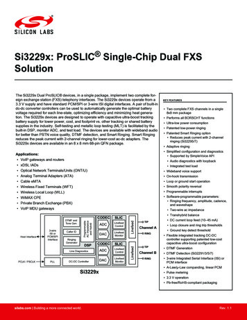
Si3229x: ProSLIC Single-Chip Dual FXSSolutionThe Si3229x Dual ProSLIC devices, in a single package, implement two complete foreign exchange station (FXS) telephony interfaces. The Si3229x devices operate from a3.3 V supply and have standard PCM/SPI or 3-wire ISI digital interfaces. A pair of built-indc-dc converter controllers can be used to automatically generate the optimal batteryvoltage required for each line-state, optimizing efficiency and minimizing heat generation. The Si3229x devices are designed to operate with capacitive ultra-boost trackingbattery supply for lower power, cost, and footprint vs. other tracking or shared batterysupplies in the industry. Self-testing and metallic loop testing (MLT) is facilitated by thebuilt-in DSP, monitor ADC, and test load. The devices are available with wideband audiofor better than PSTN voice quality, DTMF detection, and Smart Ringing. Smart Ringingreduces the peak current with 2-channel ringing for lower-cost ac-dc adapters. TheSi3229x devices are available in an 8 x 8 mm 68-pin QFN package.RingingGeneratorDSPPLL Patented low-power ringing Patented Smart Ringing option Reduces peak current with 2-channelringing (Si32295/7) Adaptive ringing Integrated test load On-hook transmission Loop or ground start operation Smooth polarity reversal Programmable interrupts Software-programmable parameters: Ringing frequency, amplitude, cadence,and waveshape Two-wire ac ODECSLICADCLinefeedControlDACLinefeedMonitorDC-DC ControllerSi3229x Transhybrid balanceLinefeedCODECLine DiagnosticsPCLK / PSCLK Ultra-low power consumption Wideband voice supportLinefeedCaller ID Performs all BORSCHT functions Audio diagnostics with loopbackProgrammableAC Impedanceand HybridHost Interface3-wireISI orPCM/SPIInterface Two complete FXS channels in a single8x8 mm package Simplified configuration and diagnostics Supported by SimpleVoice APIApplications: VoIP gateways and routers xDSL IADs Optical Network Terminals/Units (ONT/U) Analog Terminal Adapters (ATA) Cable eMTA Wireless Fixed Terminals (WFT) Wireless Local Loop (WLL) WiMAX CPE Private Branch Exchange (PBX) VoIP MDU gatewaysDTMF andTone GenKEY FEATURESTIPChannel ARINGTIPChannel BRING DC current loop feed (10–45 mA) Loop closure and ring trip thresholds Ground key detect threshold Flexible integrated tracking DC-DCcontroller supporting patented low-costcapacitive ultra-boost configuration DTMF Generation DTMF Detection (Si32291/3/5/7) 3-wire Integrated Serial Interface (ISI) orPCM interface A-Law/µ-Law companding, linear PCM Pulse metering 3.3 V operation Pb-free/RoHS-compliant packagingsilabs.com Building a more connected world.Rev. 1.1
Si3229x: ProSLIC Single-Chip Dual FXS SolutionOrdering Guide1. Ordering GuideTable 1.1. Si3229x Ordering GuideP/N1DescriptionPackage TypeMax VBATTemperatureSi32290-A-FMWideband Dual FXS, ISIinterfaceQFN682–140 V0 to 70 CSi32290-A-GMWideband Dual FXS, ISIinterfaceQFN682–140 V–40 to 85 CSi32291-A-FMWideband Dual FXS, ISIinterface, DTMF detectionQFN682–140 V0 to 70 CSi32291-A-GMWideband Dual FXS, ISIinterface, DTMF detectionQFN682–140 V–40 to 85 CSi32292-A-FMWideband Dual FXS,PCM interface, daisychain modeQFN682–140 V0 to 70 CSi32292-A-GMWideband Dual FXS,PCM interface, daisychain modeQFN682–140 V–40 to 85 CSi32293-A-FMWideband Dual FXS,PCM interface, DTMFdetection, daisy-chainmodeQFN682–140 V0 to 70 CSi32293-A-GMWideband Dual FXS,PCM interface, DTMFdetection, daisy-chainmodeQFN682–140 V–40 to 85 CSi32295-A-FMWideband Dual FXS, ISIinterface, DTMF detection, Smart RingingQFN682–140 V0 to 70 CSi32295-A-GMWideband Dual FXS, ISIinterface, DTMF detection, Smart RingingQFN682–140 V–40 to 85 CSi32297-A-FMWideband Dual FXS,PCM interface, DTMFdetection, daisy-chainmode, Smart RingingQFN682–140 V0 to 70 CSi32297-A-GMWideband Dual FXS,PCM interface, DTMFdetection, daisy-chainmode, Smart RingingQFN682–140 V–40 to 85 CSi32290-A-ZM1Wideband Dual FXS, ISIinterface, customer-specificQFN682–140 V0 to 70 CSi32291-A-ZM1Wideband Dual FXS, ISIinterface, DTMF detection, customer-specificQFN682–140 V0 to 70 Csilabs.com Building a more connected world.Rev. 1.1 2
Si3229x: ProSLIC Single-Chip Dual FXS SolutionOrdering GuideP/N1DescriptionPackage TypeMax VBATTemperatureSi32292-A-ZM1Wideband Dual FXS,PCM interface, daisychain mode, customerspecificQFN682–140 V0 to 70 CSi32293-A-ZM1Wideband Dual FXS,PCM interface, DTMFdetection, daisy-chainmode, customer-specificQFN682–140 V0 to 70 CSi32295-A-ZM1Wideband Dual FXS, ISIinterface, DTMF detection, Smart Ringing, customer-specificQFN682–140 V0 to 70 CSi32297-A-ZM1Wideband Dual FXS,PCM interface, DTMFdetection, daisy-chainmode, Smart Ringing,customer-specificQFN682–140 V0 to 70 CSi32290-A-ZM2Wideband Dual FXS, ISIinterface, customer-specificQFN682–140 V0 to 70 CSi32291-A-ZM2Wideband Dual FXS, ISIinterface, DTMF detection, customer-specificQFN682–140 V0 to 70 CSi32292-A-ZM2Wideband Dual FXS,PCM interface, daisychain mode, customerspecificQFN682–140 V0 to 70 CSi32293-A-ZM2Wideband Dual FXS,PCM interface, DTMFdetection, daisy-chainmode, customer-specificQFN682–140 V0 to 70 CSi32295-A-ZM2Wideband Dual FXS, ISIinterface, DTMF detection, Smart Ringing, customer-specificQFN682–140 V0 to 70 CSi32297-A-ZM2Wideband Dual FXS,PCM interface, DTMFdetection, daisy-chainmode, Smart Ringing,customer-specificQFN682–140 V0 to 70 CNote:1. Adding the suffix "R" to the part number (e.g., Si32292-C-FMR) denotes tape and reel.2. QFN - Quad-Flat No-leadsTable 1.2. Evaluation Kit Ordering GuidePart NumberDescriptionVBAT MaxSi32293AUB20SL0KIT2 FXS evb with lowest-cost capacitive ultraboost dc-dc converter for Si32290/1/5–140 VSi32297AUB20SL0KIT2 FXS evb with lowest-cost capacitive ultraboost dc-dc converter for Si32292/3/7–140 Vsilabs.com Building a more connected world.Rev. 1.1 3
Si3229x: ProSLIC Single-Chip Dual FXS SolutionOrdering Guide1.1 Product IdentificationThe product identification number is a finished goods part number or is specified by a finished goods part number, such as a specialcustomer part number.Si32292-A-FMRProduct DesignatorRevisionShipping OptionBlank TraysR Tape and ReelPackage Type M QFNPart Type / Lead FinishF Commercial / RoHS-CompliantG Industrial / RoHS-CompliantFigure 1.1. Example Product Identification Numbersilabs.com Building a more connected world.Rev. 1.1 4
Table of Contents1. Ordering Guide. . . . . . . . . . . . . . . . . . . . . . . . . . . . . . 21.1 Product Identification . 42. Functional Description . . . . . . . . . . . . . . . . . . . . . . . . . . . . 63. Electrical Specifications . . . . . . . . . . . . . . . . . . . . . . . . . . . 74. FXS Features. . . . . . . . . . . . . . . . . . . . . . . . . . . . . . 204.1 DC Feed Characteristics.204.2 Linefeed Operating States .204.3 Line Voltage and Current Monitoring.204.4 Power Monitoring and Power Fault Detection .204.5 Thermal Overload .204.6 Loop Closure/Ring Trip Detection.214.7 Ground Key Detection.214.8 Ringing Generation.224.9 Polarity Reversal .224.10 Two-Wire Impedance Synthesis .224.11 Transhybrid Balance Filter.22.224.13 DTMF Detection (Si32291/3/5/7 Only).224.14 Pulse Metering4.12 Tone Generators .234.15 DC-DC Controller.234.16 Wideband Audio .234.17 Test Facilities .245. System Interfaces. . . . . . . . . . . . . . . . . . . . . . . . . . . .255.1 SPI Control Interface .255.2 PCM Interface and Companding .255.3 Integrated Serial Interface .256. Pin Descriptions. . . . . . . . . . . . . . . . . . . . . . . . . . . . . 266.1 Si32290/1/5 ISI 8x8 mm Pinout.266.2 Si32292/3/7 PCM 8x8 mm Pinout.327. Packaging. . . . . . . . . . . . . . . . . . . . . . . . . . . . . . . 377.1 Package Outline: 68-Pin QFN .377.2 Land Pattern: 68-Pin QFN .397.3 Top Marking: 68-Pin QFN .408. Revision History. . . . . . . . . . . . . . . . . . . . . . . . . . . . . 42silabs.com Building a more connected world.Rev. 1.1 5
Si3229x: ProSLIC Single-Chip Dual FXS SolutionFunctional DescriptionADCLinefeedControlHost InterfacePCLK / PSCLK3-wireISI orPCM/SPIInterfaceDACLinefeedMonitorCODECSLICLine DiagnosticsADCLinefeedControlPLLDC-DC ControllerDACLinefeedMonitorCaller IDRingingGeneratorDSPLinefeedSLICProgrammableAC Impedanceand HybridCODECDTMF andTone GenLinefeed2. Functional DescriptionTIPChannel ARINGTIPChannel BRINGSi3229xFigure 2.1. Functional Block DiagramThe Si3229x dual ProSLIC devices provide all SLIC, codec, DTMF detection, and signal generation functions needed for two completeanalog telephone interfaces. They perform all battery, over-voltage, ringing, supervision, codec, hybrid, and test (BORSCHT) functions,and also support extensive metallic loop and self-test capabilities.The Si3229x supports wideband audio (150Hz-6.8kHz) compliant with PKT-SP-HDV-104-120823, and is configurable to support the fullITU-T-G.722-201209 bandwidth (50Hz-7kHz). The wideband mode provides an expanded audio band with a 16 kHz sample rate forenhanced audio quality while the standard voice-band mode provides standard telephony audio bandwidth.The Si3229x series supports either a standard PCM/SPI digital interface, or a 3-wire ISI digital interface.The Si3229x devices incorporate two programmable dc-dc converter controllers that operate in battery tracking mode. The dc-dc converter controllers react to line conditions to provide the optimal battery voltage required for each line-state. Si3229x ICs support a Vbatvoltage rating of –140 V. The Si3229x devices are available with DTMF detection and Smart Ringing. Smart Ringing provides reducedpeak current 2-channel ringing for lower-cost ac-dc adapters. See 1. Ordering Guide.Programmable on-hook voltage, programmable offhook loop current, reverse polarity operation, loop or ground start operation, and onhook transmission are supported. Loop current and voltage are continuously monitored by an integrated monitoring ADC. The Si3229xdual ProSLIC devices support ringing with or without a programmable dc offset, and can operate in low power ringing and adaptiveringing modes. The available offset, frequency, waveshape, and cadence options are designed to ring the widest variety of terminaldevices and to reduce external controller requirements.A complete audio transmit and receive path is integrated, including ac impedance and hybrid gain. These features are software-programmable, allowing a single hardware design to meet global requirements.silabs.com Building a more connected world.Rev. 1.1 6
Si3229x: ProSLIC Single-Chip Dual FXS SolutionElectrical Specifications3. Electrical SpecificationsTable 3.1. Recommended Operating ConditionsParameterSymbolTAAmbient TemperatureTest ConditionMin1TypMax1UnitF-grade02570 CG-grade–402585 CSilicon Junction Temperature, High Voltage DieTJHVContinuous——InternallyLimited CSilicon Junction Temperature, Low Voltage DieTJLVContinuous——125 CSupply VoltagesVDDA,VDDD3.133.33.47VBattery Voltage2VBAT–140—–15VNote:1. All minimum and maximum specifications apply across the recommended operating conditions. Typical values apply at nominalsupply voltages and an operating temperature of 25 C unless otherwise stated.2. Minimum and maximum battery voltage limits are dependent upon loop conditions and dc-dc converter configuration.Table 3.2. Power Supply CharacteristicsParameterSupply Currents:ResetSymbolTest ConditionMinTypMaxUnitIDDVT and VR Hi-Z , RSTB VBATSupply Currents:IDDHigh Impedance,IVBATVT and VR Hi-ZOpenSupply Currents:IDDVTR –48 V,—10.28—mAForward/Reverse,IVBATAutomatic Power Save Mode Enabled—0.4—mASupply Currents:IDDVTR -48 V,—34.40—mAForward/Reverse,IVBATAutomatic Power Save Mode Disabled—2.2—mAIDDVT or VR –48 V—10.27—mAIVBATVR or VT Hi-Z,—0.4—mAOn-hookOn-hookSupply Currents:Tip/Ring Open,On-hookSupply Currents:Tip/Ring Open,Automatic Power Save Mode EnabledIDDVT or VR -48 V—33.60—mAIVBATVR or VT Hi-Z,—1.5—mAOn-hooksilabs.com Building a more connected world.Automatic Power Save Mode DisabledRev. 1.1 7
Si3229x: ProSLIC Single-Chip Dual FXS SolutionElectrical SpecificationsParameterSupply Currents:Forward/Reverse OHT,SymbolTest ConditionMinTypMaxUnitIDDVTR 48 V—51.22—mA—3—mA—51.71—mA—2.2 ILOOP—mAIVBATOn-hookSupply Currents:Forward/Reverse Active,IDDILOOP 20 mA, RLOAD 200 ΩIVBATOff-hookSupply Currents:RingingIDDVTR 55 VRMS 0 VDC,—37.07—mAIVBATlow power ringing, sinusoidal, f 20 Hz—33.32—mARLOAD 5 REN 1400 ΩNote:1. All specifications are for a single channel of Si3229x with a low-cost capacitive boost dc-dc converter at 25 C. VDDA VDDD 3.3 V; VDC 12 V.2. IDD IDDA IDDD.Table 3.3. AC CharacteristicsParameterTest ConditionMinTypMaxUnit2-Wire - PCMSee Figure3.6 OverloadCompression Performance onpage 16.———200 Hz to 3.4 kHz (u-law/A-law)——–40dBm0200 Hz to 3.4 kHz (16-bit linear)——–63dBm0200 Hz to 3.4 kHzSee Figure3.5 Transmitand ReceivePath SNDRon page16.———46——dB——-41dB2-Wire to PCM or PCM to 2-Wire————1014 Hz, any gain setting————-0.2—0.2dBTX/RX PerformanceOverload CompressionSingle Frequency Distortion(0 dBm0 input)Signal-to-(Noise Distortion) Ratio1transmit or receive pathActive off-hook, and OHT, any ZTAudio Tone Generator Signal-toDistortion Ratio10 dBm0, Active off-hook, and OHT,any ZTIntermodulation DistortionGain Accuracy1Attenuation Distortion vs. Freq.Group Delay vs. Frequencysilabs.com Building a more connected world.0 dBm 05See Figure 3.7 Receive Path Frequency Response onpage 17 and Figure 3.8 Transmit Path Frequency Response on page 17.See Figure 3.9 Transmit Group Delay Distortion on page18 and Figure 3.10 Receive Group Delay Distortion onpage 18.Rev. 1.1 8
Si3229x: ProSLIC Single-Chip Dual FXS SolutionElectrical SpecificationsParameterTest ConditionMinTypMaxUnit1014 Hz sine wave, reference level-10 dBm————3 dB to –37 dB——0.25dB–37 dB to -50 dB——0.5dB–50 dB to -60 dB——1.0dB1014 Hz, Within same time-slot—450500μs2-Wire Return Loss3200 Hz to 3.4 kHz2630—dBTranshybrid Balance3300 Hz to 3.4 kHz2630—dBC-Message weighted—814dBrnCPsophometric weighted—–82-76dBmPRX and TX, 200 Hz to 3.4 kHz—55—dB200 Hz to 1 kHz—60—dB1 kHz to 3.4 kHz—58—dB200 Hz to 3.4 kHz at TIP or RING—50—ΩActive off-hook 60 HzReg 73 0x0B—25—mAGain Tracking2Signal level:Round-Trip Group DelayNoise PerformanceIdle Channel Noise4PSRR from VDDD, VDDA @ 3.3 VLongitudinal PerformanceLongitudinal to Metallic/PCM Balance (forward or reverse)Longitudinal ImpedanceLongitudinal Current CapabilityNote:1. Analog signal measured as VTIP - VRING. Assumes ideal line impedance matching.2. The quantization errors inherent in the μ/A-law companding process can generate slightly worse gain tracking performance in thesignal range of 3 to -37 dB for signal frequencies that are integer divisors of the 8 kHz PCM sampling rate.3. VDDD, VDDA 3.3 V, VBAT -52 V, no fuse resistors; RL 600 Ω, ZS 600 Ω synthesized using RS register coefficients.4. The level of any unwanted tones within the bandwidth of 0 to 4 kHz does not exceed -55 dBm.5. 0 dBm0 is equal to 0 dBm into 600 Ω.Table 3.4. Linefeed CharacteristicsParameterSymbolTest ConditionMinTypMaxUnitDifferential——45mACommon Mode——30mADifferential Common Mode——45mAILIM 18 mA——10%Active Mode; VOC 48 V,VTIP – VRING——4VRDOILOOP ILIM160—640ΩVOHTOIRING ILIM; VRING wrt ground,——4VDC Feed CurrentDC Loop Current AccuracyDC Open Circuit Voltage AccuracyDC Differential Output ResistanceDC On-Hook Voltage AccuracyGround Start (TIP Open)silabs.com Building a more connected world.VRING -51 VRev. 1.1 9
Si3229x: ProSLIC Single-Chip Dual FXS SolutionElectrical SpecificationsParameterSymbolTest ConditionMinTypMaxUnitDC Output Resistance-GroundStart (TIP Open)RROTOIRING ILIM;RING to ground160—640ΩDC Output Resistance-GroundStart (TIP Open)RTOTOTIP to ground400——kΩLoop Closure Detect ThresholdAccuracyITHR 13 mA——10%Ground Key Detect ThresholdAccuracyITHR 13 mA——10%Ring Trip Threshold AccuracyAC detection, VRING 70 Vpk,no offset,ITH 80 mA——4mADC detection, 20 V dc offset, ITH 13 mA——1mADC Detection, 48 V DC offset,Rloop 1500 Ω——3mAVRINGINGOpen circuit, VBAT –140 V—–138—VPKRTHD50 VRMS, 0 VOFFSET, 0–5 REN—1—%f 16 Hz to 60 Hz——1%Accuracy of ON/OFF times——50msLoop Voltage Sense AccuracyVTIP - VRING 48 V—24%Loop Current Sense AccuracyILOOP 18 mA—710%Power Threshold 1.0 WVBAT –56 V, IVDD 40 mA,RLOAD 600 Ω—15—%Ringing AmplitudeSinusoidal Ringing Total Harmonic DistortionRinging Frequency AccuracyRinging Cadence AccuracyPower Alarm Threshold AccuracyTable 3.5. Digital I/O CharacteristicsParameterSymbolTest ConditionMinTypMaxUnitHigh Level Input VoltageVIHSCLK, CSB, SPI MOSI, PCLK,FSYNC, PCM MOSI, RSTB2.0——VLow Level Input VoltageVILSCLK, CSB, SPI MOSI, PCLK,FSYNC, PCM MOSI, RSTB——0.8VHigh Level Output VoltageVOHSPI MISO, SPI MOSI THRU,PMC MISO, INTB: IO –4 mAVDDD –0.6——VLow Level Output VoltageVOLSPI MISO, SPI MOSI THRU,PMC MISO, INTB: IO 4 mA——0.4V334280μA——10μASPI MOSI THRU and RSTB Internal Pullup CurrentInput Leakage CurrentILsilabs.com Building a more connected world.Rev. 1.1 10
Si3229x: ProSLIC Single-Chip Dual FXS SolutionElectrical SpecificationsTable 3.6. Charge Pump CharacteristicsParameterSymbolTest ConditionMinTypMaxUnitOutput Voltage (DCDRVa/b,DCFFa/b)VCP2 x VDDD –1—2 x VDDDVOutput CurrentICP——31mANote:1. Peak drive current capability is 60 mA.Table 3.7. Switching Characteristics General InputsParameterSymbolMinTypMaxUnitRSTB Pulse Width (PCM/SPI or ISIInterface)tRST200——μsRSTB High to First SPI TransferStart (PCM/SPI Interface) or FirstRegister/RAM Access (ISI Interface)tRCS5——msNote:1. All timing is referenced to the 50% level of the waveform. Input test levels are VIH VDD - 0.4 V, VIL 0.4 V. Rise and Fall timesare referenced to the 20% and 80% levels of the waveform.PCM/SPI InterfacetRSTPCLKFSYNCRSTBtRCSCSBISI InterfacetRSTPSCLKRSTBtRCSRegister AccessFigure 3.1. Reset Timing Diagramsilabs.com Building a more connected world.Rev. 1.1 11
Si3229x: ProSLIC Single-Chip Dual FXS SolutionElectrical SpecificationsTable 3.8. Switching Characteristics SPIParameterSymbolMinTypMaxUnitCycle Time SCLKtc83——nsRise Time, SCLKtr——25nsFall Time, SCLKtf——25nsDelay Time, SCLK Fall to SPI MISO Activetd1——20nsDelay Time, SCLK Fall to SPI MISO Transitiontd2——20nsDelay Time, CSB Rise to SPI MISO Tristatetd3——20nsSetup Time, CSB Fall to SCLK Falltsu125——nsHold Time, CSB Rise to SCLK Riseth120——nsSetup Time, SPI MOSI Transition to SCLK Risetsu225——nsHold Time, SCLK Rise to SPI MOSI Transitionth220——nsDelay Time between Chip Selectstcs220——nsSPI MOSI to SPI MOSI THRU Propagation Delaytd4—410nsNote:1. All timing is referenced to the 50% level of the waveform. Input test levels are VIH VDDD -0.4 V, VIL 0.4 V.2. Characteristics for outputs specified with CL 20 pF.trtftcSCLKth1tsu1tcstsu2CSBth2SPI MOSItd1td2td3SPI MISOtd4SPI MOSI THRUFigure 3.2. SPI Timing Diagramsilabs.com Building a more connected world.Rev. 1.1 12
Si3229x: ProSLIC Single-Chip Dual FXS SolutionElectrical SpecificationsTable 3.9. Switching Characteristics PCM Highway InterfaceParameterPCLK PeriodPCLK Jitter er——8nsRMS—512—kHzValid PCLK MHz8.192MHzFSYNC Period4tfs—125—μsPCL
built-in DSP, monitor ADC, and test load. The devices are available with wideband audio for better than PSTN voice quality, DTMF detection, and Smart Ringing. Smart Ringing reduces the peak current with 2-channel ringing for lower-cost ac-dc adapters. The Si3229x devices are available in an