Transcription
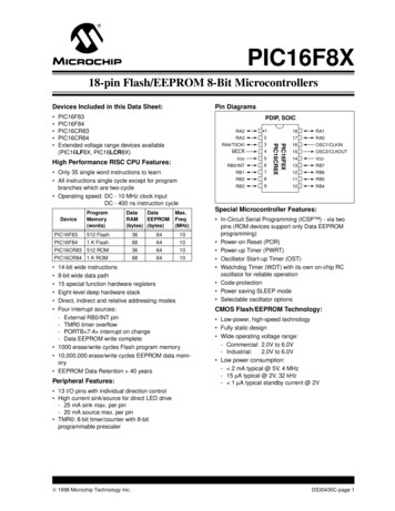
PIC16F8X18-pin Flash/EEPROM 8-Bit MicrocontrollersDevices Included in this Data Sheet:Pin DiagramsPIC16F83PIC16F84PIC16CR83PIC16CR84Extended voltage range devices available(PIC16LF8X, PIC16LCR8X)PDIP, SOICHigh Performance RISC CPU Features: Only 35 single word instructions to learn All instructions single cycle except for programbranches which are two-cycle Operating speed: DC - 10 MHz clock inputDC - 400 ns instruction ytes) (bytes)Max.Freq(MHz)PIC16F83512 Flash3664PIC16F841 K Flash686410PIC16CR83 512 ROM366410PIC16CR84 1 K ROM686410 1014-bit wide instructions8-bit wide data path15 special function hardware registersEight-level deep hardware stackDirect, indirect and relative addressing modesFour interrupt sources:- External RB0/INT pin- TMR0 timer overflow- PORTB 7:4 interrupt on change- Data EEPROM write complete 1000 erase/write cycles Flash program memory 10,000,000 erase/write cycles EEPROM data memory EEPROM Data Retention 40 yearsPeripheral Features:RA2 0RB4PIC16F8XPIC16CR8X Special Microcontroller Features: In-Circuit Serial Programming (ICSP ) - via twopins (ROM devices support only Data EEPROMprogramming) Power-on Reset (POR) Power-up Timer (PWRT) Oscillator Start-up Timer (OST) Watchdog Timer (WDT) with its own on-chip RCoscillator for reliable operation Code-protection Power saving SLEEP mode Selectable oscillator optionsCMOS Flash/EEPROM Technology: Low-power, high-speed technology Fully static design Wide operating voltage range:- Commercial: 2.0V to 6.0V- Industrial:2.0V to 6.0V Low power consumption:- 2 mA typical @ 5V, 4 MHz- 15 µA typical @ 2V, 32 kHz- 1 µA typical standby current @ 2V 13 I/O pins with individual direction control High current sink/source for direct LED drive- 25 mA sink max. per pin- 20 mA source max. per pin TMR0: 8-bit timer/counter with 8-bitprogrammable prescaler 1998 Microchip Technology Inc.DS30430C-page 1
PIC16F8XTable of Contents1.0 General Description . 32.0 PIC16F8X Device Varieties . 53.0 Architectural Overview. 74.0 Memory Organization . 115.0 I/O Ports. 216.0 Timer0 Module and TMR0 Register. 277.0 Data EEPROM Memory. 338.0 Special Features of the CPU . 379.0 Instruction Set Summary . 5310.0 Development Support . 6911.0 Electrical Characteristics for PIC16F83 and PIC16F84. 7312.0 Electrical Characteristics for PIC16CR83 and PIC16CR84. 8513.0 DC & AC Characteristics Graphs/Tables. 9714.0 Packaging Information . 109Appendix A: Feature Improvements - From PIC16C5X To PIC16F8X . 113Appendix B: Code Compatibility - from PIC16C5X to PIC16F8X. 113Appendix C: What’s New In This Data Sheet . 114Appendix D: What’s Changed In This Data Sheet . 114Appendix E: Conversion Considerations - PIC16C84 to PIC16F83/F84 And PIC16CR83/CR84. 115Index . 117On-Line Support. 119Reader Response . 120PIC16F8X Product Identification System . 121Sales and Support. 121To Our Valued CustomersWe constantly strive to improve the quality of all our products and documentation. We have spent a great deal oftime to ensure that these documents are correct. However, we realize that we may have missed a few things. If youfind any information that is missing or appears in error, please use the reader response form in the back of this datasheet to inform us. We appreciate your assistance in making this a better document.DS30430C-page 2 1998 Microchip Technology Inc.
PIC16F8X1.0GENERAL DESCRIPTIONThe PIC16F8X is a group in the PIC16CXX family oflow-cost, high-performance, CMOS, fully-static, 8-bitmicrocontrollers. This group contains the followingdevices: PIC16F83PIC16F84PIC16CR83PIC16CR84All PICmicro microcontrollers employ an advancedRISC architecture. PIC16F8X devices have enhancedcore features, eight-level deep stack, and multipleinternal and external interrupt sources. The separateinstruction and data buses of the Harvard architectureallow a 14-bit wide instruction word with a separate8-bit wide data bus. The two stage instruction pipelineallows all instructions to execute in a single cycle,except for program branches (which require twocycles). A total of 35 instructions (reduced instructionset) are available. Additionally, a large register set isused to achieve a very high performance level.PIC16F8X microcontrollers typically achieve a 2:1 codecompression and up to a 4:1 speed improvement (at 20MHz) over other 8-bit microcontrollers in their class.The PIC16F8X has up to 68 bytes of RAM, 64 bytes ofData EEPROM memory, and 13 I/O pins. A timer/counter is also available.The PIC16CXX family has special features to reduceexternal components, thus reducing cost, enhancingsystem reliability and reducing power consumption.There are four oscillator options, of which the single pinRC oscillator provides a low-cost solution, the LPoscillator minimizes power consumption, XT is astandard crystal, and the HS is for High Speed crystals.The SLEEP (power-down) mode offers power saving.The user can wake the chip from sleep through severalexternal and internal interrupts and resets.A highly reliable Watchdog Timer with its own on-chipRC oscillator provides protection against software lockup.Table 1-1 lists the features of the PIC16F8X. A simplified block diagram of the PIC16F8X is shown inFigure 3-1.The PIC16F8X fits perfectly in applications rangingfrom high speed automotive and appliance motorcontrol to low-power remote sensors, electronic locks,security devices and smart cards. The Flash/EEPROMtechnology makes customization of applicationprograms (transmitter codes, motor speeds, receiverfrequencies, security codes, etc.) extremely fast andconvenient. The small footprint packages make thismicrocontroller series perfect for all applications withspace limitations. Low-cost, low-power, highperformance, ease-of-use and I/O flexibility make thePIC16F8X very versatile even in areas where nomicrocontroller use has been considered before(e.g., timer functions; serial communication; capture,compare and PWM functions; and co-processorapplications).The serial in-system programming feature (via twopins) offers flexibility of customizing the product aftercomplete assembly and testing. This feature can beused to serialize a product, store calibration data, orprogram the device with the current firmware beforeshipping.1.1Family and Upward CompatibilityThose users familiar with the PIC16C5X family ofmicrocontrollers will realize that this is an enhancedversion of the PIC16C5X architecture. Please refer toAppendix A for a detailed list of enhancements. Codewritten for PIC16C5X devices can be easily ported toPIC16F8X devices (Appendix B).1.2Development SupportThe PIC16CXX family is supported by a full-featuredmacro assembler, a software simulator, an in-circuitemulator, a low-cost development programmer and afull-featured programmer. A “C” compiler and fuzzylogic support tools are also available.The devices with Flash program memory allow thesame device package to be used for prototyping andproduction. In-circuit reprogrammability allows thecode to be updated without the device being removedfrom the end application. This is useful in thedevelopment of many applications where the devicemay not be easily accessible, but the prototypes mayrequire code updates. This is also useful for remoteapplications where the code may need to be updated(such as rate information). 1998 Microchip Technology Inc.DS30430C-page 3
PIC16F8XTABLE 1-1PIC16F8X FAMILY OF DEVICESPIC16F83ClockMemoryMaximum Frequencyof Operation (MHz)PIC16CR8310PIC16F8410PIC16CR8410Flash Program Memory512—1K—EEPROM Program Memory————ROM Program Memory—512—1KData Memory (bytes)36366868Data EEPROM (bytes)64646464TMR0TMR0TMR0TMR0Interrupt Sources4444I/O Pins13131313Voltage Range (Volts)2.0-6.02.0-6.02.0-6.02.0-6.0Packages18-pin DIP,SOIC18-pin DIP,SOIC18-pin DIP,SOIC18-pin DIP,SOICPeripherals Timer Module(s)Features10All PICmicro Family devices have Power-on Reset, selectable Watchdog Timer, selectable code protect and high I/O current capability. All PIC16F8X Family devices use serial programming with clock pin RB6 and data pin RB7.DS30430C-page 4 1998 Microchip Technology Inc.
PIC16F8X2.0PIC16F8X DEVICE VARIETIESA variety of frequency ranges and packaging optionsare available. Depending on application and productionrequirements the proper device option can be selectedusing the information in this section. When placingorders, please use the “PIC16F8X ProductIdentification System” at the back of this data sheet tospecify the correct part number.There are four device “types” as indicated in the devicenumber.1.2.3.4.F, as in PIC16F84. These devices have Flashprogram memory and operate over the standardvoltage range.LF, as in PIC16LF84. These devices have Flashprogram memory and operate over an extendedvoltage range.CR, as in PIC16CR83. These devices haveROM program memory and operate over thestandard voltage range.LCR, as in PIC16LCR84. These devices haveROM program memory and operate over anextended voltage range.When discussing memory maps and other architecturalfeatures, the use of F and CR also implies the LF andLCR versions.2.12.3Serialized Quick-TurnaroundProduction (SQTP SM ) DevicesMicrochip offers the unique programming servicewhere a few user-defined locations in each device areprogrammed with different serial numbers. The serialnumbersmayberandom,pseudo-randomor sequential.Serial programming allows each device to have aunique number which can serve as an entry-code,password or ID number.For information on submitting a SQTP code, pleasecontact your Microchip Regional Sales Office.2.4ROM DevicesSome of Microchip’s devices have a correspondingdevice where the program memory is a ROM. Thesedevices give a cost savings over Microchip’s traditionaluser programmed devices (EPROM, EEPROM).ROM devices (PIC16CR8X) do not allow serializationinformation in the program memory space. The usermay program this information into the Data EEPROM.For information on submitting a ROM code, pleasecontact your Microchip Regional Sales Office.Flash DevicesThese devices are offered in the lower cost plasticpackage, even though the device can be erased andreprogrammed. This allows the same device to be usedfor prototype development and pilot programs as wellas production.A further advantage of the electrically-erasable Flashversion is that it can be erased and reprogrammed incircuit, or by device programmers, such as Microchip'sPICSTART Plus or PRO MATE II programmers.2.2Quick-Turnaround-Production (QTP)DevicesMicrochip offers a QTP Programming Service forfactory production orders. This service is madeavailable for users who choose not to program amedium to high quantity of units and whose codepatterns have stabilized. The devices have all Flashlocations and configuration options already programmed by the factory. Certain code and prototypeverification procedures do apply before productionshipments are available.For information on submitting a QTP code, pleasecontact your Microchip Regional Sales Office. 1998 Microchip Technology Inc.DS30430C-page 5
PIC16F8XNOTES:DS30430C-page 6 1998 Microchip Technology Inc.
PIC16F8X3.0ARCHITECTURAL OVERVIEWThe high performance of the PIC16CXX family can beattributed to a number of architectural featurescommonly found in RISC microprocessors. To beginwith, the PIC16CXX uses a Harvard architecture. Thisarchitecture has the program and data accessed fromseparate memories. So the device has a programmemory bus and a data memory bus. This improvesbandwidth over traditional von Neumann architecturewhere program and data are fetched from the samememory (accesses over the same bus). Separatingprogram and data memory further allows instructions tobe sized differently than the 8-bit wide data word.PIC16CXX opcodes are 14-bits wide, enabling singleword instructions. The full 14-bit wide program memorybus fetches a 14-bit instruction in a single cycle. A twostage pipeline overlaps fetch and execution of instructions (Example 3-1). Consequently, all instructions execute in a single cycle except for program branches.The PIC16F83 and PIC16CR83 address 512 x 14 ofprogram memory, and the PIC16F84 and PIC16CR84address 1K x 14 program memory. All program memory is internal.The PIC16CXX can directly or indirectly address itsregister files or data memory. All special functionregisters including the program counter are mapped inthe data memory. An orthogonal (symmetrical)instruction set makes it possible to carry out any operation on any register using any addressing mode. Thissymmetrical nature and lack of ‘special optimalsituations’ make programming with the PIC16CXXsimple yet efficient. In addition, the learning curve isreduced significantly. 1998 Microchip Technology Inc.DS30430C-page 7
PIC16F8XPIC16CXX devices contain an 8-bit ALU and workingregister. The ALU is a general purpose arithmetic unit.It performs arithmetic and Boolean functions betweendata in the working register and any register file.The W register is an 8-bit working register used for ALUoperations. It is not an addressable register.Depending on the instruction executed, the ALU mayaffect the values of the Carry (C), Digit Carry (DC), andZero (Z) bits in the STATUS register. The C and DC bitsoperate as a borrow and digit borrow out bit,respectively, in subtraction. See the SUBLW and SUBWFinstructions for examples.The ALU is 8-bits wide and capable of addition,subtraction, shift and logical operations. Unlessotherwise mentioned, arithmetic operations are two’scomplement in nature. In two-operand instructions,typically one operand is the working register(W register), and the other operand is a file register oran immediate constant. In single operand instructions,the operand is either the W register or a file register.FIGURE 3-1:PIC16F8X BLOCK DIAGRAMData Bus138Program CounterFlash/ROMProgramMemoryPIC16F83/CR83512 x 14PIC16F84/CR841K x 14ProgramBusA simplified block diagram for the PIC16F8X is shownin Figure 3-1, its corresponding pin description isshown in Table 3-1.8 Level Stack(13-bit)14EEPROM Data MemoryRAMFile RegistersPIC16F83/CR8336 x 8PIC16F84/CR8468 x 87EEDATARAM AddrEEPROMData Memory64 x 8EEADRAddr MuxInstruction reg7Direct Addr5TMR0IndirectAddrFSR regRA4/T0CKISTATUS reg8MUXPower-upTimerInstructionDecode &ControlTimingGenerationOscillatorStart-up Timer8ALUPower-onResetWatchdogTimerI/O PortsRA3:RA0W e 8MCLRVDD, VSS 1998 Microchip Technology Inc.
PIC16F8XTABLE 3-1PIC16F8X PINOUT C2/CLKOUT1515O—Oscillator crystal output. Connects to crystal or resonator in crystaloscillator mode. In RC mode, OSC2 pin outputs CLKOUT which has1/4 the frequency of OSC1, and denotes the instruction cycle rate.MCLR44I/PSTMaster clear (reset) input/programming voltage input. This pin is anactive low reset to the device.Pin NameBufferTypeDescriptionST/CMOS (3) Oscillator crystal input/external clock source input.PORTA is a bi-directional I/O TTLRA4/T0CKI33I/OSTCan also be selected to be the clock input to the TMR0 timer/counter. Output is open drain type.PORTB is a bi-directional I/O port. PORTB can be software programmed for internal weak pull-up on all inputs.RB0/INT66I/OTTL/ST (1)RB177I/OTTLRB288I/OTTLRB0/INT can also be selected as an external interrupt pin.RB399I/OTTLRB41010I/OTTLInterrupt on change pin.RB51111I/OTTLInterrupt on change pin.RB61212I/OTTL/ST (2)(2)TTL/STInterrupt on change pin. Serial programming clock.Interrupt on change pin. Serial programming data.RB71313I/OVSS55P—Ground reference for logic and I/O pins.VDD1414P—Positive supply for logic and I/O pins.Legend: I inputO outputI/O Input/OutputP power— Not usedTTL TTL inputST Schmitt Trigger inputNote 1: This buffer is a Schmitt Trigger input when configured as the external interrupt.2: This buffer is a Schmitt Trigger input when used in serial programming mode.3: This buffer is a Schmitt Trigger input when configured in RC oscillator mode and a CMOS input otherwise. 1998 Microchip Technology Inc.DS30430C-page 9
PIC16F8X3.1Clocking Scheme/Instruction Cycle3.2The clock input (from OSC1) is internally divided byfour to generate four non-overlapping quadratureclocks namely Q1, Q2, Q3 and Q4. Internally, theprogram counter (PC) is incremented every Q1, theinstruction is fetched from the program memory andlatched into the instruction register in Q4. Theinstruction is decoded and executed during thefollowing Q1 through Q4. The clocks and instructionexecution flow is shown in Figure 3-2.Instruction Flow/PipeliningAn “Instruction Cycle” consists of four Q cycles (Q1,Q2, Q3 and Q4). The instruction fetch and execute arepipelined such that fetch takes one instruction cyclewhile decode and execute takes another instructioncycle. However, due to the pipelining, each instructioneffectively executes in one cycle. If an instructioncauses the program counter to change (e.g., GOTO)then two cycles are required to complete the instruction(Example 3-1).A fetch cycle begins with the Program Counter (PC)incrementing in Q1.In the execution cycle, the fetched instruction is latchedinto the “Instruction Register” in cycle Q1. Thisinstruction is then decoded and executed during theQ2, Q3, and Q4 cycles. Data memory is read during Q2(operand read) and written during Q4 (destinationwrite).FIGURE 3-2:CLOCK/INSTRUCTION clockQ3Q4PCPCOSC2/CLKOUT(RC mode)EXAMPLE 3-1:Fetch INST (PC)Execute INST (PC-1)PC 2Fetch INST (PC 1)Execute INST (PC)Fetch INST (PC 2)Execute INST (PC 1)INSTRUCTION PIPELINE FLOW1. MOVLW 55h2. MOVWF PORTB3. CALL SUB 14. BSFPC 1PORTA, BIT3Fetch 1Execute 1Fetch 2Execute 2Fetch 3Execute 3Fetch 4FlushFetch SUB 1 Execute SUB 1All instructions are single cycle, except for any program branches. These take two cycles since the fetchinstruction is “flushed” from the pipeline while the new instruction is being fetched and then executed.DS30430C-page 10 1998 Microchip Technology Inc.
PIC16F8XMEMORY ORGANIZATIONThere are two memory blocks in the PIC16F8X. Theseare the program memory and the data memory. Eachblock has its own bus, so that access to each block canoccur during the same oscillator cycle.The data memory can further be broken down into thegeneral purpose RAM and the Special FunctionRegisters (SFRs). The operation of the SFRs thatcontrol the “core” are described here. The SFRs usedto control the peripheral modules are described in thesection discussing each individual peripheral module.The data memory area also contains the dataEEPROM memory. This memory is not directly mappedinto the data memory, but is indirectly mapped. That is,an indirect address pointer specifies the address of thedata EEPROM memory to read/write. The 64 bytes ofdata EEPROM memory have the address range0h-3Fh. More details on the EEPROM memory can befound in Section 7.0.4.1FIGURE 4-1:PROGRAM MEMORY MAPAND STACK - PIC16F83/CR83PC 12:0 13CALL, RETURNRETFIE, RETLWStack Level 1 Stack Level 8User MemorySpace4.0Reset Vector0000hPeripheral Interrupt Vector0004h1FFhProgram Memory OrganizationThe PIC16FXX has a 13-bit program counter capableof addressing an 8K x 14 program memory space. Forthe PIC16F83 and PIC16CR83, the first 512 x 14(0000h-01FFh)arephysicallyimplemented(Figure 4-1). For the PIC16F84 and PIC16CR84, thefirst 1K x 14 (0000h-03FFh) are physically implemented (Figure 4-2). Accessing a location above thephysically implemented address will cause a wraparound. For example, for the PIC16F84 locations 20h,420h, 820h, C20h, 1020h, 1420h, 1820h, and 1C20hwill be the same instruction.1FFFhFIGURE 4-2:PROGRAM MEMORY MAPAND STACK - PIC16F84/CR84PC 12:0 13CALL, RETURNRETFIE, RETLWStack Level 1 Stack Level 8Reset Vector0000hPeripheral Interrupt Vector0004hUser MemorySpaceThe reset vector is at 0000h and the interrupt vector isat 0004h.3FFh1FFFh 1998 Microchip Technology Inc.DS30430C-page 11
PIC16F8X4.2Data Memory Organization4.2.1GENERAL PURPOSE REGISTER FILEThe data memory is partitioned into two areas. The firstis the Special Function Registers (SFR) area, while thesecond is the General Purpose Registers (GPR) area.The SFRs control the operation of the device.All devices have some amount of General PurposeRegister (GPR) area. Each GPR is 8 bits wide and isaccessed either directly or indirectly through the FSR(Section 4.5).Portions of data memory are banked. This is for boththe SFR area and the GPR area. The GPR area isbanked to allow greater than 116 bytes of generalpurpose RAM. The banked areas of the SFR are for theregisters that control the peripheral functions. Bankingrequires the use of control bits for bank selection.These control bits are located in the STATUS Register.Figure 4-1 and Figure 4-2 show the data memory maporganization.The GPR addresses in bank 1 are mapped toaddresses in bank 0. As an example, addressing location 0Ch or 8Ch will access the same GPR.Instructions MOVWF and MOVF can move values fromthe W register to any location in the register file (“F”),and vice-versa.The special function registers can be classified into twosets, core and peripheral. Those associated with thecore functions are described in this section. Thoserelated to the operation of the peripheral features aredescribed in the section for that specific feature.The entire data memory can be accessed eitherdirectly using the absolute address of each register fileor indirectly through the File Select Register (FSR)(Section 4.5). Indirect addressing uses the presentvalue of the RP1:RP0 bits for access into the bankedareas of data memory.4.2.2SPECIAL FUNCTION REGISTERSThe Special Function Registers (Figure 4-1, Figure 4-2and Table 4-1) are used by the CPU and Peripheralfunctions to control the device operation. Theseregisters are static RAM.Data memory is partitioned into two banks whichcontain the general purpose registers and the specialfunction registers. Bank 0 is selected by clearing theRP0 bit (STATUS 5 ). Setting the RP0 bit selects Bank1. Each Bank extends up to 7Fh (128 bytes). The firsttwelve locations of each Bank are reserved for theSpecial Function Registers. The remainder are General Purpose Registers implemented as static RAM.DS30430C-page 12 1998 Microchip Technology Inc.
PIC16F8XFIGURE 4-1:REGISTER FILE MAP PIC16F83/CR83File AddressFIGURE 4-2:REGISTER FILE MAP PIC16F84/CR84File AddressFile Address80h00hIndirect ON8Bh0BhINTCONINTCON8Bh8Ch0Ch00hIndirect addr.(1)01hTMR002hPCL03h04hIndirect d(accesses)in Bank 02Fh30hFile Address8ChMapped(accesses)in Bank 04Fh50h7FhFFhBank 0Bank 1Unimplemented data memory location; read as ’0’.Note 1: Not a physical register. 1998 Microchip Technology irect addr.(1)CFhD0h7FhFFhBank 0Bank 1Unimplemented data memory location; read as ’0’.Note 1: Not a physical register.DS30430C-page 13
PIC16F8XTABLE 4-1AddressREGISTER FILE SUMMARYNameBit 7Bit 6Bit 5Bit 4Bit 3Bit 2Bit 1Bit 0Value onPower-onResetValue on allother resets(Note3)Bank 000hINDFUses contents of FSR to address data memory (not a physical register)---- -------- ----01hTMR08-bit real-time clock/counterxxxx xxxxuuuu uuuu02hPCLLow order 8 bits of the Program Counter (PC)0000 00000000 B107hC0001 1xxx000q quuuxxxx xxxxuuuu uuuuRA0---x xxxx---u uuuuRB0/INTxxxx xxxxuuuu uuuuUnimplemented location, read as '0'---- -------- ----Indirect data memory address pointer 008hEEDATAEEPROM data registerxxxx xxxxuuuu uuuu09hEEADREEPROM address registerxxxx xxxxuuuu uuuu0AhPCLATH———---0 0000---0 00000BhINTCONGIEEEIET0IE0000 000x0000 000u---- -------- ----1111 11111111 11110000 00000000 0000Write buffer for upper 5 bits of the PC (1)INTERBIET0IFINTFRBIFBank 180hINDF81hOPTIONREG82hPCL83hSTATUS (2)84hFSR85hTRISA86hTRISB87h88hEECON1Uses contents of FSR to address data memory (not a physical register)RBPUINTEDGT0CST0SEPSAPS2PS1PS0Low order 8 bits of Program Counter (PC)IRPRP1RP0TOPDZDCCIndirect data memory address pointer 0———PORTA data direction register0001 1xxx000q quuuxxxx xxxxuuuu uuuu---1 1111---1 1111PORTB data direction register1111 11111111 1111Unimplemented location, read as '0'---- -------- -------0 x000---0 IEEEIET0IEEEIFWRERRWRENWRRDEEPROM control register 2 (not a physical register)Write buffer for upper 5 bits of the PC (1)INTERBIET0IFINTFRBIF---- -------- -------0 0000---0 00000000 000x0000 000uLegend: x unknown, u unchanged. - unimplemented read as ’0’, q value depends on condition.Note 1: The upper byte of the program counter is not directly accessible. PCLATH is a slave register for PC 12:8 . The contentsof PCLATH can be transferred to the upper byte of the program counter, but the contents of PC 12:8 is never transferredto PCLATH.2: The TO and PD status bits in the STATUS register are not affected by a MCLR reset.3: Other (non power-up) resets include: external reset through MCLR and the Watchdog Timer Reset.DS30430C-page 14 1998 Microchip Technology Inc.
PIC16F8X4.2.2.1STATUS REGISTERThe STATUS register contains the arithmetic status ofthe ALU, the RESET status and the bank select bit fordata memory.As with any register, the STATUS register can be thedestination for any instruction. If the STATUS register isthe destination for an instruction that affects the Z, DCor C bits, then the write to these three bits is disabled.These bits are set or cleared according to device logic.Furthermore, the TO and PD bits are not writable.Therefore, the result of an instruction with the STATUSregister as destination may be different than intended.For example, CLRF STATUS will clear the upper-threebits and set the Z bit. This leaves the STATUS registeras 000u u1uu (where u unchanged).FIGURE 4-1:R/W-0IRPOnly the BCF, BSF, SWAPF and MOVWF instructionsshould be used to alter the STATUS register (Table 9-2)because these instructions do not affect any status bit.Note 1: The IRP and RP1 bits (STATUS 7:6 ) ar
All PICmicro microcontrollers employ an advanced RISC architecture. PIC16F8X devices have enhanced core features, eight-level deep stack, and multiple internal and external interrupt sources. The separate instruction and data buses of the Harvard architecture allow a 14-bit wide instruction word with a separate 8-bit wide data bus.