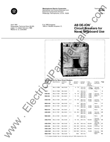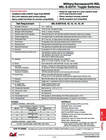
Transcription
REVISIONSLTRDESCRIPTIONDATE (YR-MO-DA)APPROVEDAAdd vendor CAGE F8859. Add device class V criteria. Add case outline X.Add table III, delta limits. Update boilerplate. Editorial changes throughout. –ltg00-07-12Raymond MonninBAdd section 1.5, radiation features. Move VIH and VIL from table I to section1.4. Add appendix A, microcircuit die. Update the boilerplate toMIL-PRF-38535 requirements and to include radiation hardness assuredrequirements. Editorial changes throughout. – TVN05-02-08Thomas M. HessCCorrect wafer thickness in appendix A. – LTG07-03-07Thomas M. HessDAdd new device type 02. For device type 01 add footnote 8/ in section 1.5 andadd Table IB for SEP test limits. Add paragraph 4.4.4.2 single eventphenomena for device type 01. Update boilerplate to current requirements ofMIL-PRF- 38535. MAA08-12-19Thomas M. HessEMake change to footnote 6/ in section 1.3. Update boilerplate paragraphs tothe current MIL-PRF- 38535 requirements. - LTG12-02-22Thomas M. HessFAdd transition supply current (Icct) test for device type 02 to table IA. Updatetitle of this drawing. - MAA12-09-07Thomas M. HessGAdd new device type 03. Add new die for device type 03. - MAA13-04-16Thomas M. HessHAdd case outline Y to section 1.2.4 for device types 01 and 03. Updateboilerplate paragraphs to the current requirements of MIL-PRF-38535. - MAA18-03-22Thomas M. HessJUpdate footnote 6/ in section 1.3. - MAA18-06-12Thomas M. HessCURRENT CAGE CODE 2425REV STATUSREVJJJJJJJJJJJJJJOF SHEETSSHEET1234567891011121314PMIC N/APREPARED BYJames E. NicklausSTANDARDMICROCIRCUITDRAWINGCHECKED BYD. A. DiCenzoAPPROVED BYN. A. HauckTHIS DRAWING IS AVAILABLEFOR USE BY ALLDEPARTMENTSAND AGENCIES OF THEDEPARTMENT OF DEFENSEAMSC N/ADLA LAND AND MARITIMECOLUMBUS, OHIO G APPROVAL DATE87-05-15REVISION LEVELJMICROCIRCUIT, DIGITAL, ADVANCED CMOS,RADIATION HARDENED, HEX INVERTER, SCHMITTTRIGGER, MONOLITHIC SILICONSIZECAGE CODEA14933DSCC FORM 2233APR 97DISTRIBUTION STATEMENT A. Approved for public release. Distribution is unlimited.Downloaded from Arrow.com.SHEET5962-876241 OF 255962-E441-18
1. SCOPE1.1 Scope. This drawing documents two product assurance class levels consisting of high reliability (device classes Q andM) and space application (device class V). A choice of case outlines and lead finishes are available and are reflected in the Partor Identifying Number (PIN). When available, a choice of Radiation Hardness Assurance (RHA) levels is reflected in the PIN.1.2 PIN. The PIN is as shown in the following examples.For device classes M and Q:5962-Federalstock classdesignator\RHAdesignator(see 1.2.1)8762401CADevicetype(see 1.2.2)Caseoutline(see 1.2.4)Leadfinish(see 1.2.5)/\/Drawing numberFor device class V:5962FFederalstock classdesignator\RHAdesignator(see 1.2.1)8762401VXADevicetype(see 1.2.2)Deviceclassdesignator(see 1.2.3)Caseoutline(see 1.2.4)Leadfinish(see 1.2.5)/\/Drawing number1.2.1 RHA designator. Device classes Q and V RHA marked devices meet the MIL-PRF-38535 specified RHA levels and aremarked with the appropriate RHA designator. Device class M RHA marked devices meet the MIL-PRF-38535, appendix Aspecified RHA levels and are marked with the appropriate RHA designator. A dash (-) indicates a non-RHA device.1.2.2 Device type(s). The device type(s) identify the circuit function as follows:Device typeGeneric numberCircuit function0154AC14Hex inverter, Schmitt trigger0254AC14-SPHex inverter, Schmitt-trigger0354AC14-SPHex inverter, Schmitt-trigger1.2.3 Device class designator. The device class designator is a single letter identifying the product assurance level as listedbelow. Since the device class designator has been added after the original issuance of this drawing, device classes M and Qdesignators will not be included in the PIN and will not be marked on the device.Device classMQ or VDevice requirements documentationVendor self-certification to the requirements for MIL-STD-883 compliant, nonJAN class level B microcircuits in accordance with MIL-PRF-38535, appendix ACertification and qualification to MIL-PRF-38535STANDARDMICROCIRCUIT DRAWINGDLA LAND AND MARITIMECOLUMBUS, OHIO 43218-3990DSCC FORM 2234APR 97Downloaded from Arrow.com.SIZE5962-87624AREVISION LEVELJSHEET2
1.2.4 Case outline(s). The case outline(s) are as designated in MIL-STD-1835 and as follows:Outline letterCD2XYDescriptive designatorTerminalsGDIP1-T14 or CDIP2-T14GDFP1-F14 or CDFP2-F14CQCC1-N20CDFP3-F14CDFP3-F14Package style1414201414Dual-in-lineFlat packLeadless chip carrierFlat pack 9/Flat pack 10/1.2.5 Lead finish. The lead finish is as specified in MIL-PRF-38535 for device classes Q and V or MIL-PRF-38535,appendix A for device class M.1.3 Absolute maximum ratings. 1/ 2/ 3/Supply voltage range (VCC) . -0.5 V dc to 7.0 V dcDC input voltage range (VIN) . -0.5 V dc to VCC 0.5 V dc 6/DC output voltage range (VOUT) . -0.5 V dc to VCC 0.5 V dc 6/Clamp diode current (IIK, IOK) . 20 mADC output current (IOUT) . 50 mADC VCC or GND current (per pin) for device type 01 . 50 mAContinuous current through VCC or GND for device types 02 and 03. 200 mAMaximum power dissipation (PD) . 500 mWStorage temperature range (TSTG) . -65 C to 150 CLead temperature (soldering, 10 seconds):Case outline X . 260 COther case outlines (except case outline X) . 245 CThermal resistance, junction-to-case (θJC) . See MIL-STD-1835Junction temperature (TJ) . 175 C 4/1.4 Recommended operating conditions. 2/ 3/ 5/ 7/Supply voltage range (VCC) . 2.0 V dc to 6.0 V dcInput voltage range (VIN) . 0.0 V dc to VCCOutput voltage range (VOUT). 0.0 V dc to VCCMinimum high level input voltage (VIH) for device types 01, 02 and 03:at VCC 3.0 V . 2.1 Vat VCC 4.5 V . 3.15 Vat VCC 5.5 V . 3.85Maximum low level input voltage (VIL) for device types 01, 02 and 03:at VCC 3.0 V . 0.9 Vat VCC 4.5 V . 1.35 Vat VCC 5.5 V . 1.65 VMaximum high level output current (IOH) for device type 01, 02 and 03:at VCC 3.0 V . -12.0 mAat VCC 4.5 V . -24.0 mAat VCC 5.5 V . -24.0 mAMaximum low level output current (IOL) for device type 01, 02 and 03:at VCC 3.0 V . 12.0 mAat VCC 4.5 V . 24.0 mAat VCC 5.5 V . 24.0 mACase operating temperature range (TC) . -55 C to 125 CSTANDARDMICROCIRCUIT DRAWINGDLA LAND AND MARITIMECOLUMBUS, OHIO 43218-3990DSCC FORM 2234APR 97Downloaded from Arrow.com.SIZE5962-87624AREVISION LEVELJSHEET3
1.5 Radiation features.Device types 01 and 03:Maximum total dose available (dose rate 50 – 300 Rad (Si)/s) . 300K Rad (Si)No Single event latch-up (SEL) occurs at effective LET (see 4.4.4.2) . 93 MeV-cm2/mg 8/1/Stresses above the absolute maximum rating may cause permanent damage to the device. Extended operation at themaximum levels may degrade performance and affect reliability.2/Unless otherwise specified, all voltages are referenced to GND.3/The limits for the parameters specified herein shall apply over the full specified VCC range and case temperature rangeof -55 C to 125 C.4/Maximum junction temperature shall not be exceeded except for allowable short duration burn-in screening conditions inaccordance with method 5004 of MIL-STD-883.5/Operation from 2.0 V dc to 3.0 V dc is provided for compatibility with data retention and battery back-up systems. Dataretention implies no input transition and no stored data loss with the following conditions: VIH 70% VCC, VIL 30% VCC,VOH 70% VCC @ -20 µA VOL 30% VCC @ 20 µA.6/The input and output voltage ratings for device types 01 and 02 (for vendor CAGE 01295) and device types 01 and 03 (forvendor CAGE F8859) may be exceeded provided the input and output current ratings are observed.7/All unused inputs of the device types 01, 02 and 03 must be held at VCC or GND to ensure proper device operation.8/Limits are guaranteed by design or process but not production tested unless specified by the customer through thepurchase order or contract.9/ Package case outline X flat pack with isolated lid.10/ Package case outline Y flat pack with grounded lid.STANDARDMICROCIRCUIT DRAWINGDLA LAND AND MARITIMECOLUMBUS, OHIO 43218-3990DSCC FORM 2234APR 97Downloaded from Arrow.com.SIZE5962-87624AREVISION LEVELJSHEET4
2. APPLICABLE DOCUMENTS2.1 Government specification, standards, and handbooks. The following specification, standards, and handbooks form a partof this drawing to the extent specified herein. Unless otherwise specified, the issues of these documents are those cited in thesolicitation or contract.DEPARTMENT OF DEFENSE SPECIFICATIONMIL-PRF-38535 - Integrated Circuits, Manufacturing, General Specification for.DEPARTMENT OF DEFENSE STANDARDSMIL-STD-883 MIL-STD-1835 -Test Method Standard Microcircuits.Interface Standard Electronic Component Case Outlines.DEPARTMENT OF DEFENSE HANDBOOKSMIL-HDBK-103 MIL-HDBK-780 -List of Standard Microcircuit Drawings.Standard Microcircuit Drawings.(Copies of these documents are available online at http://quicksearch.dla.mil).2.2 Non-Government publications. The following document(s) form a part of this document to the extent specified herein.Unless otherwise specified, the issues of these documents cited in the solicitation or contract.JEDEC – SOLID STATE TECHNOLOGY ASSOCIATION (JEDEC)JEDEC Standard JESD20 - Standard for Description of 54/74ACXXXXX and 54/74ACTXXXXX Advanced High-SpeedCMOS Devices.(Copies of these documents are available online at https://www.jedec.org or from JEDEC – Solid State TechnologyAssociation, 3103 North 10th Street, Suite 240-S Arlington, VA 22201).2.3 Order of precedence. In the event of a conflict between the text of this drawing and the references cited herein, the textof this drawing takes precedence. Nothing in this document, however, supersedes applicable laws and regulations unless aspecific exemption has been obtained.3.1 Item requirements. The individual item requirements for device classes Q and V shall be in accordance withMIL-PRF-38535 and as specified herein or as modified in the device manufacturer's Quality Management (QM) plan. Themodification in the QM plan shall not affect the form, fit, or function as described herein. The individual item requirements fordevice class M shall be in accordance with MIL-PRF-38535, appendix A for non-JAN class level B devices and as specifiedherein.3.1.1 Microcircuit die. For the requirements of microcircuit die, see appendix A to this document.3.2 Design, construction, and physical dimensions. The design, construction, and physical dimensions shall be as specifiedin MIL-PRF-38535 and herein for device classes Q and V or MIL-PRF-38535, appendix A and herein for device class M.STANDARDMICROCIRCUIT DRAWINGDLA LAND AND MARITIMECOLUMBUS, OHIO 43218-3990DSCC FORM 2234APR 97Downloaded from Arrow.com.SIZE5962-87624AREVISION LEVELJSHEET5
3.2.1 Case outlines. The case outlines shall be in accordance with 1.2.4 herein.3.2.2 Terminal connections. The terminal connections shall be as specified on figure 1.3.2.3 Truth table. The truth table shall be as specified on figure 2.3.2.4 Logic diagram. The logic diagram shall be as specified on figure 3.3.2.5 Switching waveforms and test circuit. The switching waveforms and test circuit shall be as specified on figure 4.3.2.6 Radiation exposure circuit. The radiation exposure circuit shall be maintained by the manufacturer under documentrevision level control and shall be made available to the preparing and acquiring activity upon request.3.3 Electrical performance characteristics and postirradiation parameter limits. Unless otherwise specified herein, theelectrical performance characteristics and postirradiation parameter limits are as specified in table IA and shall apply over thefull case operating temperature range.3.4 Electrical test requirements. The electrical test requirements shall be the subgroups specified in table IIA. The electricaltests for each subgroup are defined in table IA.3.5 Marking. The part shall be marked with the PIN listed in 1.2 herein. In addition, the manufacturer's PIN may also bemarked. For packages where marking of the entire SMD PIN number is not feasible due to space limitations, the manufacturerhas the option of not marking the "5962-" on the device. For RHA product using this option, the RHA designator shall still bemarked. Marking for device classes Q and V shall be in accordance with MIL-PRF-38535. Marking for device class M shall bein accordance with MIL-PRF-38535, appendix A.3.5.1 Certification/compliance mark. The certification mark for device classes Q and V shall be a "QML" or "Q" as required inMIL-PRF-38535. The compliance mark for device class M shall be a "C" as required in MIL-PRF-38535, appendix A.3.6 Certificate of compliance. For device classes Q and V, a certificate of compliance shall be required from a QML-38535listed manufacturer in order to supply to the requirements of this drawing (see 6.6.1 herein). For device class M, a certificate ofcompliance shall be required from a manufacturer in order to be listed as an approved source of supply in MIL-HDBK-103(see 6.6.2 herein). The certificate of compliance submitted to DLA Land and Maritime-VA prior to listing as an approved sourceof supply for this drawing shall affirm that the manufacturer's product meets, for device classes Q and V, the requirements ofMIL-PRF-38535 and herein or for device class M, the requirements of MIL-PRF-38535, appendix A and herein.3.7 Certificate of conformance. A certificate of conformance as required for device classes Q and V in MIL-PRF-38535 or fordevice class M in MIL-PRF-38535, appendix A shall be provided with each lot of microcircuits delivered to this drawing.3.8 Notification of change for device class M. For device class M, notification to DLA Land and Maritime-VA of change ofproduct (see 6.2 herein) involving devices acquired to this drawing is required for any change that affects this drawing.3.9 Verification and review for device class M. For device class M, DLA Land and Maritime, DLA Land and Maritime's agent,and the acquiring activity retain the option to review the manufacturer's facility and applicable required documentation. Offshoredocumentation shall be made available onshore at the option of the reviewer.3.10 Microcircuit group assignment for device class M. Device class M devices covered by this drawing shall be inmicrocircuit group number 36 (see MIL-PRF-38535, appendix A).STANDARDMICROCIRCUIT DRAWINGDLA LAND AND MARITIMECOLUMBUS, OHIO 43218-3990DSCC FORM 2234APR 97Downloaded from Arrow.com.SIZE5962-87624AREVISION LEVELJSHEET6
TABLE IA. Electrical performance characteristics.Test andMIL-STD-883test method 1/High level outputvoltage3006Low level outputvoltage3007SymbolVOH5/VOL5/Test conditions 2/ 3/-55 C TC 125 C 3.0 V VCC 5.5 Vunless otherwise specifiedDevice typeanddevice classVCCGroup AsubgroupsLimits 4/MinUnitMaxFor all inputs affecting outputunder test,VIN VIH minimum orVIL maximumFor all other inputs,VIN VCC or GNDIOH -50 µAAllAll3.0 V1, 2, 32.9VAllAll4.5 V1, 2, 34.4AllAll5.5 V1, 2, 35.4For all inputs affecting outputunder test, VIN VIH minimum orVIL maximum. For all other inputs,VIN VCC or GND;IOH -12 mAAllAll3.0 V1, 2, 32.4For all inputs affecting outputunder test, VIN VIH minimum orVIL maximum. For all other inputs,VIN VCC or GNDIOH -24 mAAllAll4.5 V1, 2, 33.7AllAll5.5 V1, 2, 34.7For all inputs affecting outputunder test, VIN VIH minimum orVIL maximum. For all other inputs,VIN VCC or GNDIOH -50 mAAllAll5.5 V1, 2, 33.85For all inputs affecting outputunder test, VIN VIH minimum orVIL maximumFor all other inputs,VIN VCC or GNDIOL 50 µAAllAll3.0 V1, 2, 30.1AllAll4.5 V1, 2, 30.1AllAll5.5 V1, 2, 30.1For all inputs affecting outputunder test, VIN VIH minimum orVIL maximum. For all other inputs,VIN VCC or GNDIOL 12 mAAllAll3.0 V1, 2, 30.5For all inputs affecting outputunder test, VIN VIH minimum orVIL maximumFor all other inputs, VIN VCC orGNDIOL 24 mAAllAll4.5 V1, 2, 30.5AllAll5.5 V1, 2, 30.5For all inputs affecting outputunder test, VIN VIH minimum orVIL maximum. For all other inputs,VIN VCC or GNDIOL 50 mAAllAll5.5 V1, 2, 31.65VSee footnotes at end of table.STANDARDMICROCIRCUIT DRAWINGDLA LAND AND MARITIMECOLUMBUS, OHIO 43218-3990DSCC FORM 2234APR 97Downloaded from Arrow.com.SIZE5962-87624AREVISION LEVELJSHEET7
TABLE IA. Electrical performance characteristics - Continued.Test andMIL-STD-883test method 1/Positive-goingthreshold voltageNegative-goingthreshold voltageHysteresis voltageSymbolTest conditions 2/ 3/-55 C TC 125 C 3.0 V VCC 5.5 Vunless otherwise specifiedDevice typeanddevice classVCCGroup AsubgroupsLimits 4/MinVT UnitMax02All3.0 V1, 2, 32.301, 03All3.0 V1, 2, 32.2AllAll4.5 V1, 2, 33.2AllAll3.0 VVT-VHYS5.5 VV3.91, 2, 30.54.5 V0.95.5 V1.1V02All3.0 V1, 2, 30.31.301, 03All3.0 V1, 2, 30.31.2AllAll4.5 V1, 2, 30.41.40.51.65.5 VVPositive inputclamp voltage3022VIC For input under test,IIN 1.0 mAAllAll0.0 V10.41.5VNegative inputclamp voltage3022VIC-For input under test, IIN -1.0 mAAllAllOpen1-0.4-1.5VFor input under test, VIN VCCFor all other inputs,VIN VCC or GNDAllAll5.5 V10.1µA2, 31.0For input under test, VIN GNDFor all other inputs,VIN VCC or GNDAllAll5.5 V1-0.12, 3-1.0For all inputs, VIN VCC or GNDIO 0 AAllAll5.5 V14.02, 380.0150.014.02, 380.0150.01, 2, 37.5Input current high3010IIHInput current low3009IILQuiescent supplycurrent, outputhigh3005ICCHM, D, P, L, R, F 6/Quiescent supplycurrent, outputlow3005ICCLFor all inputs, VIN VCC or GNDIO 0 AM, D, P, L, R, F 6/Transition supplycurrentICCt01, 03Q, VFor input under test, VIN VCC/2For all other inputs,VIN VCC or GND 10/AllAll5.5 V01, 03Q, V02, 03All5.5 VµAµAµAmASee footnotes at end of tableSTANDARDMICROCIRCUIT DRAWINGDLA LAND AND MARITIMECOLUMBUS, OHIO 43218-3990DSCC FORM 2234APR 97Downloaded from Arrow.com.SIZE5962-87624AREVISION LEVELJSHEET8
TABLE IA. Electrical performance characteristics - Continued.Test andMIL-STD-883test method 1/SymbolTest conditions 2/ 3/-55 C TC 125 C 3.0 V VCC 5.5 Vunless otherwise specifiedDevice typeanddevice classVCCGroup AsubgroupsLimits 4/MinUnitMaxInput capacitance3012CINSee 4.4.1cTC 25 CAllAll5.0 V48.0pFPower dissipationcapacitanceCPD7/See 4.4.1cTC 25 CAllAll5.0 V450.0pFFor all inputs,VIN VIH minimum orVIL maximumVerify output VOUTSee 4.4.1bAllAll3.0 V7, 8LHAllAll5.5 V7, 8LHCL 50 pF minimumRL 500ΩSee figure 401All3.0 V91.011.510, 111.014.091.08.510, 111.010.091.511.510, 111.014.0Functional test3014Propagation delaytime, An to Yn30038/tPHL9/4.5 V02, 03AlltPLH9/CL 50 pF minimumRL 500ΩSee figure 401All3.0 Vand3.6 V4.5 Vand5.5 V91.58.510, 111.510.03.0 V91.013.510, 111.016.091.010.010, 111.012.091.513.510, 111.016.091.510.010, 111.512.04.5 V02, 03All3.0 Vand3.6 V4.5 Vand5.5 Vnsns1/For tests not listed in the referenced MIL-STD-883, [e.g. VT , VT-], utilize the general test procedure under the conditionslisted herein.2/Each input/output, as applicable, shall be tested at the specified temperature, for the specified limits, to the tests in table IAherein. Output terminals not designated shall be high level logic, low level logic, or open, except as follows:a. For VIC tests, the GND terminal can be open. TC 25 C.b. For VIC- tests, the VCC terminal shall be open. TC 25 C.c. For all ICC tests, the output terminal shall be open. When performing these tests, the current meter shall be placedin the circuit such that all current flows through the meter.The values to be used for VIH minimum and VIL maximum shall be those values listed in section 1.4 herein.STANDARDMICROCIRCUIT DRAWINGDLA LAND AND MARITIMECOLUMBUS, OHIO 43218-3990DSCC FORM 2234APR 97Downloaded from Arrow.com.SIZE5962-87624AREVISION LEVELJSHEET9
TABLE IA. Electrical performance characteristics - Continued.3/RHA devices for device types 01 and 03 have been characterized through all levels M, D, P, L, R, and F of irradiation.However, this device is only tested at the “F” level. Pre and post irradiation values are identical unless otherwise specifiedin table IA. When performing post irradiation electrical measurements for any RHA level, TA 25 C.4/For negative and positive voltage and current values, the sign designates the potential difference in reference to GND andthe direction of current flow, respectively; and the absolute value of the magnitude, not the sign, is relative to the minimumand maximum limits, as applicable, listed herein. All devices shall meet or exceed the limits specified in table IA, asapplicable, at 3.0 V VCC 3.6 V and 4.5 V VCC 5.5 V.5/The VOH and VOL tests shall be tested at VCC 3.0 V and 4.5 V. The VOH and VOL tests are guaranteed, if not tested, forother values of VCC. Limits shown apply to operation at VCC 3.3 V 0.3 V and VCC 5.0 V 0.5 V. Tests with inputcurrent at 50 mA and –50 mA are performed on only one input at a time with duration not to exceed 10 ms. Transmissiondriving tests may be performed using VIN VCC or GND. When VIN VCC or GND is used, the test is guaranteed for VIN VIH minimum and VIL maximum.6/The maximum limit for this parameter at 100K Rad (Si) is 4 µA.7/Power dissipation capacitance (CPD) determines both the power consumption (PD) and dynamic current consumption (IS).Where:PD (CPD CL) (VCC x VCC) f (ICC x VCC)IS (CPD CL) VCC* f ICCFor both PD and IS, f is the frequency of the input signal and CL is the external output load capacitance.8/Tests shall be performed in sequence, attributes data only. Functional tests shall include the truth table and other logicpatterns used for fault detection. The test vectors used to verify the truth table shall, at a minimum, test all functions ofeach input and output. All possible input to output logic patterns per function shall be guaranteed, if not tested, to the truthtable in figure 2 herein. Functional tests shall be performed in sequence as approved by the qualifying activity on qualifieddevices. Allowable tolerances in accordance with MIL-STD-883 for the input voltage levels may be incorporated. Foroutputs measurements, H 0.7 VCC, L 0.3 VCC.9/The AC limits at VCC 5.5 V are equal to the limits at VCC 4.5 V and guaranteed by testing at VCC 4.5 V. The AC limitsat VCC 3.6 V are equal to the limits at VCC 3.0 V and guaranteed by testing at VCC 3.0 V. Minimum AC limits forVCC 5.5 V and VCC 3.6 V are 1.0 ns and guaranteed by guard banding the VCC 4.5 V and VCC 3.0 V minimum limits,respectively, to 1.5 ns. For propagation delay tests, all paths must be tested.10/ The input VIN increment in 0.1V steps to 3.7V.TABLE IB. SEP test limits.1/ 2/DevicetypeSEPTA temperature 10 CBias VCCEffective LET01, 03No SEL 125 C5.5 VLET 93 MeV-cm2/mg1/ For SEP test conditions, see 4.4.4.2 herein.2/ Technology characterization and model verification supplemented by in-line data may be used in lieu ofend-of-line testing. Test plan must be approved by TRB and qualifying activity.STANDARDMICROCIRCUIT DRAWINGDLA LAND AND MARITIMECOLUMBUS, OHIO 43218-3990DSCC FORM 2234APR 97Downloaded from Arrow.com.SIZE5962-87624AREVISION LEVELJSHEET10
DevicetypeCaseoutlinesAllC, D, X and YTerminalnumber2Terminal ---NC18---6Y19---6A20---VCCNC No internal connections.Note: Package case outline X flat pack with isolated lid. Package case outline Y flat pack with grounded lid.FIGURE 1. Terminal connections.STANDARDMICROCIRCUIT DRAWINGDLA LAND AND MARITIMECOLUMBUS, OHIO 43218-3990DSCC FORM 2234APR 97Downloaded from Arrow.com.SIZE5962-87624AREVISION LEVELJSHEET11
Each inverterInputOutputAYHLLHH High voltage levelL Low voltage levelFIGURE 2. Truth table.FIGURE 3. Logic diagram.STANDARDMICROCIRCUIT DRAWINGDLA LAND AND MARITIMECOLUMBUS, OHIO 43218-3990DSCC FORM 2234APR 97Downloaded from Arrow.com.SIZE5962-87624AREVISION LEVELJSHEET12
NOTES:1. CL 50 pF minimum or equivalent (includes probe and jig capacitance).2. RL 500Ω or equivalent.3. Input signal from pulse generator: VIN 0.0 V to VCC; PRR 1 MHz; ZO 50Ω; tr 3.0 ns; tf 3.0 ns; tr and tf shall bemeasured from 10% of VCC to 90% of VCC and from 90% of VCC to 10% of VCC, respectively; duty cycle 50 percent.4. Timing parameters shall be tested at a minimum input frequency of 1MHz.5. The outputs are measured one at a time with one transition per measurement.FIGURE 4. Switching waveforms and test circuit.STANDARDMICROCIRCUIT DRAWINGDLA LAND AND MARITIMECOLUMBUS, OHIO 43218-3990DSCC FORM 2234APR 97Downloaded from Arrow.com.SIZE5962-87624AREVISION LEVELJSHEET13
4. VERIFICATION4.1 Sampling and inspection. For device classes Q and V, sampling and inspection procedures shall be in accordance withMIL-PRF-38535 or as modified in the device manufacturer's Quality Management (QM) plan. The modification in the QM planshall not affect the form, fit, or function as described herein. For device class M, sampling and inspection procedures shall be inaccordance with MIL-PRF-38535, appendix A.4.2 Screening. For device classes Q and V, screening shall be in accordance with MIL-PRF-38535, and shall be conductedon all devices prior to qualification and technology conformance inspection. For device class M, screening shall be inaccordance with method 5004 of MIL-STD-883, and shall be conducted on all devices prior to quality conformance inspection.4.2.1 Additional criteria for device class M.a.Burn-in test, method 1015 of MIL-STD-883.(1) Test condition A, B, C, or D. The test circuit shall be maintained by the manufacturer under document revisionlevel control and shall be made available to the preparing or acquiring activity upon request. The test circuit shallspecify the inputs, outputs, biases, and power dissipation, as applicable, in accordance with the intent specified inmethod 1015.(2) TA 125 C, minimum.b.Interim and final electrical test parameters shall be as specified in table IIA herein.4.2.2 Additional criteria for device classes Q and V.a.The burn-in test duration, test condition and test temperature, or approved alternatives shall be as specified in thedevice manufacturer's QM plan in accordance with MIL-PRF-38535. The burn-in test circuit shall be maintained underdocument revision level control of the device manufacturer's Technology Review Board (TRB) in accordance withMIL-PRF-38535 and shall be made available to the acquiring or preparing activity upon request. The test circuit shallspecify the inputs, outputs, biases, and power dissipation, as applicable, in accordance with the intent specified inmethod 1015 of MIL-STD-883.b.Interim and final electrical test parameters shall be as specified in table IIA herein.c.Additional screening for device class V beyond the requirements of device class Q shall be as specified inMIL-PRF-38535, appendix B.4.3 Qualification inspection for device classes Q and V. Qualification inspection for device classes Q and V shall be inaccordance with MIL-PRF-38535. Inspections to be performed shall be those specified in MIL-PRF-38535 and herein for groupsA, B, C, D, and E inspections (see 4.4.1 through 4.4.4).4.4 Conformance inspection. Technology conformance inspection for classes Q and V shall be in accordance withMIL-PRF-38535 including groups A, B, C, D, and E inspections and as specified. Quality conformance inspection for deviceclass M shall be in accordance with MIL-PRF-38535, appendix A and as specified herein. Inspections to be performed fordevice class M shall be those specified in method 5005 of MIL-STD-883 a
accordance with method 5004 of MIL-STD -883, and shall be conducted on all devices prior to quality conformance inspection. 4.2.1 A dditional criteria for device class M . a. Burn-in test, method 1015 of MIL-STD -883. (1) Test condition A, B, C, or D . The test circuit shall be maintained by the manufacturer under document revision