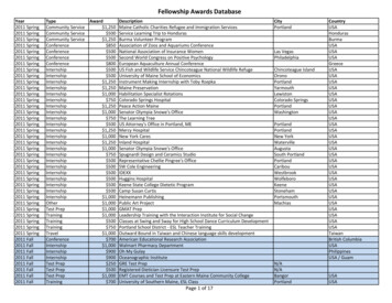
Transcription
Summer Internship: Project ReportSubmitted By:JAYANT THATTERoll No.:EE09B109Company:BITMAPPER INTEGRATION TECHNOLOGIES PVT. LTD.Industry:VLSI/FPGA PLATFORM DEVELOPMENTAbstractThe first week of the internship period was spent in revising basic concepts of VHDL and Verilogcoding. I was also introduced to other hardware design related issues like static timing analysis,simulations, synthesis and basics of PLDs (internal architecture, various types etc.). To get betteracquainted with the design and coding techniques, various test-codes were written for testing thevarious peripherals (starting from basic LED testing and including tests for ADC, DAC, RS232 andFlash memory testing). Through these codes, I got well acquainted with Xilinx design tools such asISE, Plan Ahead as well as Altera tools like Quartus and more advanced NIOS.After getting well-versed with design techniques, the project for designing a QDR Controller IP wasstarted. The IP consisted of hardware design code and application software. The hardware designcode was written in VHDL and implemented on Xilinx Spartan 6 FPGA. The application software waswritten in C programming language to transact data and commands between computer and theFPGA. At the end of the designing phase, the Controller was tested at a satisfactory data rate ofabout 100 megabytes per second on the Spartan 6 FPGA. Designing and successful testing of thiscontroller took about 5 weeks.The last two weeks were spent in studying and understanding the EMIF (External Memory Interface)bus, which is used to interface DSP with its peripherals including FPGA. After acquiring a detailedunderstanding of the EMIF bus, an application was written to accept data from ADC (interfaced toXilinx Vertex 4 FPGA) and to transfer it to Texas Instruments DSP. This data was then looped backusing the EMIF bus and displayed live on Oscilloscope through DAC interfaced again to FPGA. Thedata taken from ADC can be output to DAC using the EMIF interface after the data is processed bythe DSP.
Table of ContentsAbstract . 0QDR Controller IP . 2Basics of QDR . 2Timing Issues . 2Outline of the Hardware Design . 2Specifications . 2Design Details. 2Application Software. 4Tests Performed . 4EMIF Bus Application . 4Basics of EMIF Bus. 4Design Details: Board Specifications . 4Basic Codes . 5FPGA Program . 5DSP Program . 6Programming DSP PLL using GEL File . 6Basics of GEL File . 6DSP Registers to be Programmed using GEL File . 6Configuring DSP Timing Characteristics . 7Tests . 7References . 7
QDR Controller IPBasics of QDRA QDR is a type of SRAM that can transfer up to four words in every clock cycle, hence the nameQuad Data Rate memory. QDR memory has separate ports for read and write and each port is DualData Rate (DDR). The main purpose of QDR is that it enables fast and independent reads and writes,at high clock frequencies without losing bandwidth in due to bus turnaround time as opposed toDDR memories.Timing IssuesEach port of a Quad Data Rate memory transacts data twice every clock cycle and is designed tooperate at high frequencies (typically few hundred MHz) in burst mode, whereas a designimplemented on FPGA cannot operate at this frequency. This is one of the main challenges in FPGAdesigns involving QDR. This problem was overcome by making use of input/output DDRs† (ODDRand IDDR). Timing is a very critical issue in QDR designs. Hence, softwares such as Xilinx Plan Aheadwere used to achieve a good timing performance.† An ODDR accepts two clock inputs (typically a differential clock) and two data inputs, each of themlatched on the rising edge of the respective clock. This data then comes to the output via amultiplexer which passes the inputs alternately. Thus an ODDR accepts data from two inputs at agiven frequency and outputs data at twice the frequency. An IDDR functions exact opposite of ODDR.It accepts input at a given frequency and gives two outputs at half the frequency.Outline of the Hardware DesignThe various steps involved are:1. Implementing the design file by file in ISE2. Download .bit file into Spartan 6 FPGA3. Checking read and write functionality using GUI based softwareSpecifications Cypress CY7C15632KV18 Quad Data Rate memory, 72 Mbit, 4 word burst Xilinx Spartan 6 FPGADesign DetailsGiven below is the block diagram of the QDR Controller IP.Data sent by the application software interfaced passed on to the FPGA via USB connection. Thedata is accepted within the FPGA in a USB controller. USB controller consists of two FIFOs, one whichaccepts data from the USB and the other which sends data to USB. The two FIFOs are controlled byread/write logic of the USB controller.The command structure consisted of a start byte and an end byte, three bytes each for passing thefile size and start address and one byte for the actual command (in this case read or write). Thecommand is decoded in the instruction decoder and important information such as the startingaddress, file size, read/write etc. are sent to the QDR read-write module.
Figure 1: Top Level Block DiagramThe QDR read-write module accepts data coming from USB and passes it on to QDR via ODDRsduring the write operation. Similarly, during a read operation, data is read from QDR and passed toUSB controller through IDDR. The ODDRs and IDDRs help in reducing the frequency at which FPGAmust operate for desired data transaction rate in QDR. Data transacted to or from the QDR usingstate machines written after taking into consideration the timing characteristics of the QDR memorychip.Figure 2: Detailed Block diagram
Application SoftwareCommands are accepted from the computer via the application software. The command is thenprocessed in hardware and data is read from or written to the QDR memory accordingly. Theapplication software reads data from the test files and sends data to USB using 512 byte buffer.Similarly, data is accepted from USB into the buffer and then written to the output file. The inputand output files are compared to test the read and write operations performed on QDR memory.Tests Performed Simple Counter Test: Serial values were written to serial memory locations, read back andverified.Data Loopback: After the counter test was successful, the developed IP was tested throughread/write loopback testing for files of various sizes. The IP gave a satisfactory performancewith a data rate of about 100 megabytes per second.EMIF Bus ApplicationBasics of EMIF BusEMIF stands for external memory interface. It is an interface used to connect DSP processors tovarious peripherals. All devices connected to DSP are mapped in a memory map. DSP is able tocommunicate with these devices by writing appropriate values to various control registers of theEMIF bus and by reading or writing data to the correct address locations in this memory map.FPGA DSP interface is a little more complicated as both FPGA as well as DSP need to beprogrammed. DSP is programmed with an application program written in C , while the FPGA isprogrammed with .bit file.Design Details: Board Specifications FPGA: Xilinx Virtex 4 (XC4VSX55-FF1148) having 55,296 logic cells.DSP: DaVinci Processor from Texas Instruments (TMS320DM6467).ADC: High Speed ADC (ADS5527) 4 channels. 12 bit Analog to Digital Converter from Texas Instruments. Sampling Speed – 210 Msps. Analog Input range - 2 Vpp. DAC: High Speed DAC (AD9742) 4 channels. 12 bit Digital to Analog Converter from Texas Instruments. Sampling Speed – 210 Msps. Analog Input range - 2 Vpp. EMIF Bus: 16 bit data width, Asynchronous.
Basic CodesFPGA ProgramFPGA is programmed using the .bit file in FOLDER . Data is accepted from ADC into a FIFO. Theclock-out given by ADC is used as write clock for this FIFO. Data from this FIFO is sent to DSP usingthe bi-directional EMIF (External Memory Interface) bus. From DSP data is looped back using thesame EMIF bus. This data is accepted in another FIFO from where it is read by DAC. The SYNC-clockfor DAC is used as read clock for this DAC-FIFO.Figure 3: Top Level Block DiagramFigure 4: Detail Block Diagram
DSP ProgramDSP is coded using Code Composer Studio Version 4. Data is accepted from FPGA using EMIF bus andthen sent back using the same bus. Single data is read and then written immediately. Only after theprevious data is written back to FPGA, next data is read from it. This is done to maintain acontinuous supply of data to the DAC.Programming DSP PLL using GEL FileBasics of GEL FileGEL file is a C program file which the DSP uses to configure itself before loading the user applicationprogram. GEL file is loaded into the DSP at the beginning of “Debug” session in CCSv4. Writingcorrect setting in the GEL file is necessary for proper functioning of the application program in DSP.DSP Registers to be Programmed using GEL FilePLL Control Register (PLL CTL) Function: Controls all the important settings of PLL Location: This is a 32 bit register located at address 0x01C40900. Setting: CLKMODE (bit 8): To be set to 1 if using external clock source for PLL (as in our case). PLLENSRC (bit 5): This bit must be cleared before PLLEN will have any effect. PLLDIS(bit 4): Setting this bit disables PLL. When using PLL this bit must be cleared. PLLRST(bit 3): Making this bit 0 asserts reset to PLL. When using PLL this bit must 1. PLLPWRDN (bit 1): Make this bit 1 to power down PLL; 0 for normal operation. PLLEN(bit 0): PLL is bypassed when this bit is cleared. Set this bit to use PLL. PLL Initialization: Following steps must be followed in your GEL file to initialize PLL.1. Set clock mode (CLKMODE)2. Set PLL to bypass, wait for PLL to stabilize (PLLEN 0, wait)3. Reset PLL (PLLRST 0)4. Disable PLL (PLLDIS 1)5. Power up PLL (PLLPWRDN 0)6. Enable PLL (PLLDIS 0)7. Wait for PLL to stabilize8. Load PLL multiplier (Refer PLLM register)9. Set PLL post dividers (Refer PLLDIVn registers)10. Wait for PLL to reset (PLLRST 0, wait)11. Release from reset (PLLRST 1)12. Wait for PLL to re-lock13. Switch out of bypass mode (PLLEN 1)PLL Multiplier Control Register (PLLM) Function: Controls PLL multiplier value Location: This is a 32 bit register located at address 0x01C40910. Setting: Multiplier value PLLM (4 : 0) 1 Note: There is an allowable range for PLL multiplier (PLLM). There is a minimum andmaximum operating frequency for DEV MXI/DEV CLKIN, PLLOUT, AUX MXI/AUX CLKIN,
and the device clocks (SYSCLKs). The PLL Controllers must be configured not to exceed any ofthese constraints documented in this section (certain combinations of external clock inputs,internal dividers, and PLL multiply ratios might not be supported). For our device allowedmultiplier values are between 14 and 22. PLLM value used in the code is 21 implying amultiplier value of 22.PLL Divider Control Registers (PLLDIVn)PLLDIVn controls divider value for SYSCLKn. EMIF bus runs on SYSCLK3. Default value of PLLDIV3 is 4.Values for PLLDIV1, 2, 3 are fixed while others are programmable.Configuring DSP Timing Characteristics Function: DSP timing characteristics can be configured writing appropriate values toAsynchronous n Configuration Registers (AnCR). There are four such registers, one for eachselect space. For our application the register corresponding to FPGA (CS4/A3CR) wasconfigured. Location: This is a 32 bit register located at address 0x20008018. Setting: EW (bit 30): Bit must be cleared to disable Extended Wait. The bit should NOT be set ifthe device does not have an EM WAIT pin. W SETUP (bits 29:26): Write Setup Time (W SETUP 1)*EMIF Clock Period. W STROBE (bits 25:20): Write Strobe Width (W STROBE 1)*EMIF Clock Period. W HOLD (bits 19:17): Write Hold Time (W HOLD 1)*EMIF Clock Period. R SETUP (bits 16:13): Read Setup Time (R SETUP 1)*EMIF Clock Period. R STROBE (bits 12:7): Read Strobe Width (R STROBE 1)*EMIF Clock Period. R HOLD (bits 6:4): Read Hold Time (R HOLD 1)*EMIF Clock Period. TA (bits 3:2): Bus Turn Around Time (TA 1)*EMIF Clock Period. ASIZE (bits 1:0): 00 if EMIF bus width is 8 bit, 01 if 16 bit. Note: EMIF Clock is DaVinci SYSCLK3. The frequency of this clock may be calculated knowingthe PLL setting (enabled/bypassed), multiplier values.TestsLive data loopback takes place at a rate of about 400 kHz. Signals fed into ADC can be viewed on anoscilloscope. Signals with frequencies up to 200 kHz get looped back successfully (with little or noglitches). Signals of higher frequencies get somewhat degraded.References Xilinx DocumentationCypress CY7C15632KV18 DatasheetFTDI Chip FT2232H DatasheetInterfacing Xilinx FPGAs to TI DSP Platforms using EMIF Bus: XAPP753 (v2.0.1)TMS320DM646x User Guide for Asynchronous EMIF (sprueq7c)Creating Device Initialisation GEL fIles (SPRAA74A)Code Composer Studio v4 Documentation
Summer Internship: Project Report Submitted By: JAYANT THATTE Roll No.: EE09B109 Company: BITMAPPER INTEGRATION TECHNOLOGIES PVT. LTD. Industry: VLSI/FPGA PLATFORM DEVELOPMENT Abstract The first week of the internship period was spent in revising basic concepts of VHDL and Verilog