Transcription
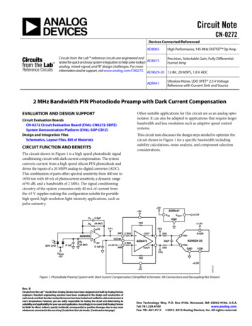
Circuit NoteCN-0272Devices Connected/ReferencedAD8065High Performance, 145 MHz FASTFET Op AmpCircuits from the Lab reference circuits are engineered andPrecision, Selectable Gain, Fully Differentialtested for quick and easy system integration to help solve today’s AD8475Funnel Ampanalog, mixed-signal, and RF design challenges. For moreinformation and/or support, visit www.analog.com/CN0272. AD9629-20 12-Bit, 20 MSPS, 1.8 V ADCUltralow Noise, LDO XFET 2.5 V VoltageReference with Current Sink and SourceADR4412 MHz Bandwidth PIN Photodiode Preamp with Dark Current CompensationEVALUATION AND DESIGN SUPPORTOther suitable applications for this circuit are as an analog optoisolator. It can also be adapted to applications that require largerbandwidth and less resolution such as adaptive speed controlsystems.Circuit Evaluation BoardsCN-0272 Circuit Evaluation Board (EVAL-CN0272-SDPZ)System Demonstration Platform (EVAL-SDP-CB1Z)Design and Integration FilesSchematics, Layout Files, Bill of MaterialsThis circuit note discusses the design steps needed to optimize thecircuit shown in Figure 1 for a specific bandwidth includingstability calculations, noise analysis, and component selectionconsiderations.CIRCUIT FUNCTION AND BENEFITSThe circuit shown in Figure 1 is a high speed photodiode signalconditioning circuit with dark current compensation. The systemconverts current from a high speed silicon PIN photodiode anddrives the inputs of a 20 MSPS analog-to-digital converter (ADC).This combination of parts offers spectral sensitivity from 400 nm to1050 nm with 49 nA of photocurrent sensitivity, a dynamic rangeof 91 dB, and a bandwidth of 2 MHz. The signal conditioningcircuitry of the system consumes only 40 mA of current fromthe 5 V supplies making this configuration suitable for portablehigh speed, high resolution light intensity applications, such aspulse oximetry. 5VADR441 5VVINCF3.3pFRF24.9kΩ 5V1kΩTP3INP 2.5kΩVOCM0.1µFRF24.9kΩ–5V0.1µF 1.8VTP1AD8065SFH 2701 2.5VVOUTGND2.5kΩ 2.5V–OUTAD8475INNVBIAS–5V33Ω OUT22pF33ΩVIN–AVDDAD9629-20VIN GNDVCMTP21kΩ–5V10599-001 0.9VFigure 1. Photodiode Preamp System with Dark Current Compensation (Simplified Schematic: All Connections and Decoupling Not Shown)Rev. BCircuits from the Lab circuits from Analog Devices have been designed and built by Analog Devicesengineers. Standard engineering practices have been employed in the design and construction ofeach circuit, and their function and performance have been tested and verified in a lab environment atroom temperature. However, you are solely responsible for testing the circuit and determining itssuitability and applicability for your use and application. Accordingly, in no event shall Analog Devicesbe liable for direct, indirect, special, incidental, consequential or punitive damages due to any causewhatsoever connected to the use of any Circuits from the Lab circuits. (Continued on last page)One Technology Way, P.O. Box 9106, Norwood, MA 02062-9106, U.S.A.Tel: 781.329.4700www.analog.comFax: 781.461.3113 2012–2013 Analog Devices, Inc. All rights reserved.
CN-0272Circuit NoteCFRFCIN CS CD CMRSH 1011ΩIPHOTOCMCSCDCM0.1µF10599-002VBVORFFigure 2. Wideband Photodiode Preamp Equivalent Circuit for AC and Noise AnalysisCIRCUIT DESCRIPTIONComponent SelectionPhotodiodes are high impedance sensors used to detect theintensity of light. Photodiodes do not have internal gain but canoperate at much higher light levels than other light detectors.Photodiodes operate either with zero bias (photovoltaic mode)or with a reverse bias (photoconductive mode). The most preciselinear operation is obtained in the photovoltaic mode, whilehigher switching speeds are realizable when the diode is operatedin the photoconductive mode at the expense of linearity. Underthese reverse bias conditions, a small amount of current calleddark current flows even when there is no illumination. The darkcurrent error can be cancelled using a second photodiode of thesame type in the noninverting input of the op amp as is shownin Figure 1.Three factors influence the response time of a photodiode The charge collection time of the carriers in the depletedregion of the photodiodeThe charge collection time of the carriers in the undepletedregion of the photodiodeThe RC time constant of the diode circuit combinationBecause the junction capacitance is dependent on the diffused areaof the photodiode and the applied reverse bias, faster rise times areobtained with smaller diffused area photodiodes and larger appliedreverse biases. The junction capacitance for the SFH 2701 PINphotodiode used in the CN-0272 circuit note is 3 pF typical, 5 pFmaximum for 0 V bias. The typical capacitance is 2 pF for 1 Vreverse bias and 1.7 pF for 5 V reverse bias. Measurements inthe circuit were all taken with a reverse bias of 5 V.Where IPHOTO is the output current of the photodiode, and theparallel combination of RF and CF sets the signal bandwidth. Ideally,all of the output current from the photodiode passes through RF,but all op amps have input bias currents that introduce errors onthe output. Op amps with picoamps of input bias current and lowinput offset voltages are preferred to minimize the error. TheAD8065 has only 2 pA of input bias current and only 400 µV ofinput offset voltage.The circuit is designed to have a full scale output of 5 V with amaximum photodiode current of 200 µA. This determines thevalue of the feedback resistor to beRF 5 V/200 µA 24.9 kΩThe stable bandwidth attainable with this preamp is a function ofRF, the gain bandwidth product of the amplifier (65 MHz), and thetotal capacitance at the amplifier’s summing junction, CIN. Forthis circuit, the SFH 2701 diode (OSRAM Opto SemiconductorsGmbH) has a maximum capacitance of CD 5 pF. The AD8065common-mode input capacitance is CM 2.1 pF, and thedifferential-mode input capacitance is CD 4.5 pF. Therefore,the total input capacitance is CIN 11.6 pF.It can be shown that the signal bandwidth resulting in a 45 phase margin, f(45), is defined byf (45) 5.7 MHzBecause the maximum attainable bandwidth is larger than theintended bandwidth, the AD8065 is a good candidate for theapplication, which is largely due to its large ratio of fCR to CIN.Figure 2 shows an I/V converter with an electrical model of aphotodiode. The basic transfer function isVOUT 65 MHzf CR 2π RF C IN2π 24.9 kΩ 11.6 pFI PHOTO RF1 sC F RFRev. B Page 2 of 8
Circuit NoteCN-0272The resistor noise is calculated using the Johnson noise formula.RF and CIN produce a pole in the loop transfer function of theamplifier that can result in peaking and instability (see Figure 3).Adding CF creates a zero in the loop transfer function thatcompensates for the effect of the pole and reduces the signalbandwidth.f1 1*2πRF(CF CIN)VRF RTO 4kTRF 1.57 f 2 36 μV rmswhere:k is Boltzmann’s constant (1.38 10-23J/K).T is the absolute temperature in Kelvin.The factor of 1.57 converts the approximate single-pole bandwidthinto the equivalent noise bandwidth.*IF (CIN) CF,THEN CF CAN BE OMITTED1f2 2πR CF FCF Note that the 0.1 µF capacitor on the positive input of the preampeliminates the high frequency noise produced by the second RFresistor used to cancel the effects of bias current.CIN2πR FfCROPEN LOOP GAINGAINThe primary source of output noise is due to the input voltage noiseand the high frequency noise gain peaking that occurs betweenf1 and fCR. If it is assumed that the output noise is constant overthe entire range of frequencies and the maximum value for theac noise gain is used, thenUNCOMPENSATEDf2COMPENSATEDNOISE DUETO AMPLIFIER CVNRTO VN 1 INCF f1fCRVEN10599-0031FREQUENCY (Hz)Figure 3. Compensation for Input Capacitancewhere VN is the input voltage noise of the amplifier (7 nV/ Hz).The total rms noise referred to the output is then the RSS valueof the two componentsThe value of CF that produces 2 MHz of bandwidth with theselected value of RF isCF Total RTO Noise 11 3.3 pF2πRF f 2 2π 24.9 kΩ 2 MHzTo determine if 3.3 pF is enough capacitance to stabilize the system,calculate the amount of capacitance needed to obtain 45 of phasemargin. The value of CF that produces f(45) can be shown as11.6 pFC IN CF 2π RF f CR2π 24.9 kΩ 65 MHz 1.57 f 2 56 μV rms (36)2 (56)2 67 μV rmsThe total output dynamic range of the preamp can be calculatedby dividing the full scale output signal (5 V) by the total outputrms noise (67 µV rms) and converting it to decibels, yieldingapproximately 97 dB.Dynamic Range 20 log(5 V/67 µV)) 97 dBADC SelectionBecause the amount of noise output by the amplifier is knownthe maximum number of bits that can be resolved can now becalculated by dividing the full scale output by the rms noise. 1.1 pFTotal RMS LSBs 5 V/67 µV 74,627Because the intended value of 3.3 pF is larger than the minimumvalue of 1.1 pF, the system is stable because increasing thecapacitance increases the amount of phase margin.The number of rms LSBs can be converted into effectiveresolution.Noise AnalysisEffective Resolution log2(74,627) 16.19 BitsNow that the components are selected, how much resolution isneeded to convert the signal must be determined. As in mostnoise analyses, only the key contributors need to be identified.Noise sources combine in an RSS manner; therefore, any singlenoise source that is at least three-to-four times larger than anyof the others dominates.Noise-free code resolution can be obtained by subtracting2.7 bits from effective resolution.In the case of the photodiode preamp, the dominant sources ofoutput noise are the input voltage noise of the op amp and thefeedback resistor noise. The input current noise of the FET-inputop amp is negligible. The shot noise of the photodiode (causedby reverse bias) is negligible because of the filtering effect of theshunt capacitance.Depending on the end application, 13 bits may be more resolutionthan is actually needed. Because the intended application doesnot require this amount of resolution, it has been confirmedthat the system meets the design requirements with 12 bits.Noise-Free Code Resolution Effective Resolution – 2.7 Bits 16.19 Bits – 2.7 Bits 13.49 BitsRev. B Page 3 of 8
CN-0272Circuit NoteIf the LSB size (in current) is smaller than the amount of darkcurrent, as mentioned earlier, the dark current can be canceledusing a second photodiode of the same type in the noninvertinginput of the op amp. For example, if 16 bits of resolution isneeded, the amount of photocurrent detected isILSB The output noise due to the AD8475 is calculated by multiplyingthe output noise density (10nV/ Hz) by the square root of thebandwidth set by the output filter.Output Filter BW I PHOTO 200 μA 3 nA2N21611 110 MHz2πRC 2π 66 Ω 22pFNoise at AD8475 Output After Filter 10 nV/ Hz Since the maximum amount of dark current that flows in theSFH 2701 is specified at 5 nA, dark current compensation isneeded in a 16-bit design.(1.57 110 MHz) 131 μV rmsThe total noise at the output of the AD8475 after the filter iscalculated by taking the RSS value of the two components isThis application uses a 12-bit ADC; therefore, the LSB size is49 nA, and it does not require dark current compensation.Total Noise If the bandwidth is 2 MHz, a reasonable guideline is to select anADC with a sampling rate 10 times greater or more. This meansthe ideal ADC must sample at a rate of 20 MSPS with 12 bits ofresolution.With the noise contribution of the AD8475 incorporated intothe calculations, the number of bits that can be resolved can beconfirmed, and the total dynamic range can be calculated.Total RMS LSBs 5 V/134 µV 37,313The AD9629-20 is a good candidate because it is a 20 MSPS ADCwith 12 bits of resolution. However, it requires differential inputs,and the 5 V p-p single-ended signal must be converted to a2 V p-p differential signal. This is easily accomplished by usingthe AD8475 differential funnel amplifier, which simplifies thesingle-ended-to-differential conversion, and provides commonmode level shifting and precision attenuation.The AD8475 has only a 500 µV maximum output offset, a10 nV/ Hz differential output noise, and 112 dB totalharmonic distortion plus noise (THD N).The AD8475 can support a maximum output voltage of 2 V p-p upto 10 MHz, which is well within the design requirement of 2 MHz.The gain of the AD8475 was determined by the analog input spanof the AD9629-20 (2 V p-p) and the full scale output of theAD8065 (5 V p-p).(27)2 (131)2 134 μV rmsEffective Resolution log2(37,313) 15.19 BitsNoise-Free Code Resolution Effective Resolution – 2.7 Bits 15.19 Bits – 2.7 Bits 12.49 BitsDynamic Range 20 log(5 V/134 µV)) 91 dBTest ResultsA laser diode was used to drive the D1 photodiode and generatea current. Photodiode D2 is used for dark current compensationand is covered with an optically opaque epoxy (EPO-TEK 320)to prevent output current from D2 when D1 is excited.By forcing the photodiode to drive a larger than expected current,the approximate maximum rise and fall time of the AD8065 was72 ns (see Figure 4).Gain 2 V p-p/5 V p-p 0.4It is important to include the noise contribution of the AD8475in this system. This is calculated by first multiplying the outputnoise of the AD8065 (67 µV rms) by the gain of the AD8475 toget the contribution due to the AD8065.Noise at AD8475 Output due to Noise of AD8065 0.4 67 µV rms 27 µV rms5V0V10599-004An on-chip, common-mode voltage of 0.9 V is included in theAD9629-20 and is available from the VCM pin. This pin drivesthe VOCM pin of the AD8475 with the common-mode voltageof 0.9 V.CH4 1.00VTM200ns2.470µsA CH44.73VFigure 4. Pulse Response by Overdriving the PhotodiodeRev. B Page 4 of 8
Circuit NoteCN-0272A more realistic rise and fall time of the system can be measured bymoving the position of the laser diode so that it does not overdrivethe photodiode current beyond 200 µA. Figure 5 shows themeasured rise and fall time of the AD8065 to be 282 ns and 290 ns,respectively. It is important to note that there is no ringing afterthe laser diode has turned off in both test cases because there issufficient phase margin.10599-0075VFigure 7. Screenshot of CN0272 Evaluation Software Digitizing a 2 MHzVarying Light Source10599-0050VCH4 1.00VTM200ns98.00nsA CH4A complete design support package for this circuit note can befound at gure 5. Pulse Response of Laser DiodeNow that the response of the system to a pulse of bright light hasbeen tested, how the system responds to high speed changes inlight intensity can be tested. An Agilent 33250A function generatorwas used to drive a laser diode with a 2 MHz sine wave. Figure 6shows that the output of the AD8065 was able to successfullydetect the small changes in light intensity, and Figure 7 showsa screenshot of the CN0272 Evaluation Software successfullyreceiving conversion data from the AD9629-20 ADC andplotting the data in a chart.3VA pulse oximeter is a medical device used for continuouslymeasuring the percentage of hemoglobin (Hgb) saturated withoxygen and the pulse rate of a patient. Hemoglobin carryingoxygen (oxyhemoglobin) absorbs light in the infrared region(940 nm) of the spectrum; hemoglobin that is not carryingoxygen (deoxyhemoglobin) absorbs visible red light (650 nm).The percentage of oxygen in the body is determined by calculatingthe ratio between these two intensities of light.In a pulse oximeter, two LEDs (one emitting red light and theother emitting infrared light) are rapidly and sequentially excitedby two current sources and a photodiode is used to detect theintensity of the light from the LEDs. The circuit shown in Figure 1can be synchronized with an LED current sink circuit, such asthe CN-0125, to capture the light from each LED as it transmitsthrough the tissue10599-0060VApplications in Pulse OximetryCH2 500mVTM200ns0.0sA CH21.65VFigure 6. Output of AD8065 Using a Varying Light SourceRev. B Page 5 of 8
CN-0272Circuit NoteCOMMON VARIATIONSFunctional Block DiagramOther suitable dual supply amplifiers are the ADA4817-1 andADA4637-1. If single supply operation is required, the AD8605 orthe AD8615 are suggested. These amplifiers all have less than 2 pAof input bias current, less than 400 µV of input offset, and morethan 10 MHz of unity-gain bandwidth products.See Figure 1 for the circuit block diagram and the EVAL-CN0272SDPZ-PADSSchematic-RevC.pdf file for the complete circuitschematic. This file is contained in the CN-0272 DesignSupport Package.EVAL-CFTL-6V-PWRZ6V WALL WARTFor applications requiring 100 MHz of bandwidth or greater,such as adaptive speed control, the combination of the ADA4817-1FastFET amplifier, the ADA4932-1 low power differential ADCdriver, and the 12-bit, 210 MSPS AD9634-210 ADC are suggested.The ADA4817-1 has a high gain bandwidth product of 400 MHzand extremely small input capacitance of 1.4 pF. This makes theamplifier ideal for wideband transimpedance applications.J3D1GNDCIRCUIT EVALUATION AND TESTThe following equipment is needed: A PC with a USB port and Windows XP (32 bit),Windows Vista , or Windows 7The EVAL-CN0272-SDPZ circuit boardThe EVAL-SDP-CB1Z SDP-B controller boardThe CN-0272 SDP Evaluation SoftwareThe EVAL-CFTL-6V-PWRZ dc power supply or equivalent6 V/1 A bench supplyA light source between 400 nm to 1050 nmGetting StartedLoad the evaluation software by placing the CN0272 evaluationsoftware into the CD drive of the PC. Using My Computer, locatethe drive that contains the evaluation software.120PINSD2EVAL-CN0272-SDPZBOARDEquipment NeededUSBTP1The ADA4932-1 driver can maintain 2 V p-p outputs up to360 MHz, which is sufficient for the AD9634-210 ADC.This circuit uses the EVAL-CN0272-SDPZ circuit board andthe EVAL-SDP-CB1Z SDP-B System Demonstration Platformcontroller board. The two boards have 120-pin mating connectors,allowing for the quick setup and evaluation of the performanceof the circuit. The EVAL-CN0272-SDPZ board contains the circuitto be evaluated, as described in this note, and the SDP-B controllerboard is used with the CN0272 Evaluation Software to capturethe data from the EVAL-CN0272-SDPZ circuit board.PCJ4CON AEVAL-SDP-CB1ZSDP-B Board10599-008The components selected were optimized for noise and cost;however, other combinations can be substituted.Figure 8. Test Setup Block DiagramSetupConnect the 120-pin connector on the EVAL-CN0272-SDPZcircuit board to the CON A connector on the EVAL-SDP-CB1Zcontroller board (SDP-B). Use nylon hardware to firmly securethe two boards, using the holes provided at the ends of the 120-pinconnectors. With power to the supply off, connect a 6 V powersupply to the 6 V and GND pins on the board. If available, a 6 Vwall wart can be connected to the barrel connector on the boardand used in place of the 6 V power supply. Connect the USB cablesupplied with the SDP-B board to the USB port on the PC. Do notconnect the USB cable to the Mini-USB connector on the SDP-Bboard at this time.TestApply power to the 6 V supply (or wall wart) connected to theEVAL-CN0272-SDPZ circuit board. Launch the evaluationsoftware and connect the USB cable from the PC to the Mini-USBconnector on the SDP-B board.Once USB communications are established, the SDP-B boardcan be used to send, receive, and capture parallel data from theEVAL-CN0272-SDPZ board.Figure 9 shows a photo of the EVAL-CN0272-SDPZ evaluationboard connected to the SDP board. Information regarding theSDP-B board can be found in the SDP-B User Guide.Note that photodiode D2 is used for dark current compensationand is covered with an optically opaque epoxy (EPO-TEK 320)to prevent output current from D2 when D1 is excited.Information and details regarding test setup and calibration, andhow to use the evaluation software for data capture can be found inthe CN-0272 Software User Guide.Rev. B Page 6 of 8
CN-027210599-009Circuit NoteFigure 9. EVAL-CN0272-SDPZ Evaluation Board Connected to the EVAL-SDP-CB1Z SDP-B BoardConnectivity for Prototype DevelopmentThe EVAL-CN0272-SDPZ evaluation board is designed to use theEVAL-SDP-CB1Z SDP-B board; however, any microprocessor canbe used to interface to the parallel peripheral interface (PPI) ofthe AD9629-20. In order for another controller to be used withthe EVAL-CN0272-SDPZ evaluation board, software must bedeveloped by a third party.There are existing interposer boards that can be used to interface tothe Altera and Xilinx field programmable gate arrays (FPGAs).The BeMicro SDK board from Altera can be used with theBeMicro SDK/SDP interposer using Nios Drivers. Any Xilinxevaluation board that features the FMC connector can be usedwith the FMC-SDP Interposer board.Rev. B Page 7 of 8
CN-0272Circuit NoteLEARN MOREData Sheets and Evaluation BoardsCN-0272 Design Support Package:CN-0272 Circuit Evaluation Board (EVAL-CN0272-SDPZ)System Demonstration Platform (EVAL-SDP-CB1Z)http://www. analog. com/CN0272-DesignSupportSDP-B User GuideAD8065 DatasheetArdizzoni, John. A Practical Guide to High-Speed Printed-CircuitBoard Layout, Analog Dialogue 39-09, September 2005.AD8475 DatasheetKester, Walt, Wurcer, Scott, Kitchin, Chuck. High ImpedanceSensors, Practical Design Techniques for Sensor SignalConditioning, Section 5, 1999.AD9629-20 DatasheetADR441 DatasheetREVISION HISTORYMT-004 Tutorial, The Good, the Bad, and the Ugly Aspects ofADC Input Noise—Is No Noise Good Noise? Analog Devices.MT-031 Tutorial, Grounding Data Converters and Solving theMystery of “AGND” and “DGND”, Analog Devices.MT-035, Op Amp Inputs, Outputs, Single-Supply, and Rail-toRail Issues, Analog Devices.11/13—Rev. A to Rev. BChanges to Figure 3 .3Changes to Figure 7 .512/12—Rev. 0 to Rev. AChanges to Test Section .611/12—Revision 0: Initial VersionMT-036 Tutorial, Op Amp Output Phase-Reversal and InputOver-Voltage Protection, Analog Devices.MT-068 Tutorial, Difference and Current Sense Amplifiers,Analog Devices.MT-101 Tutorial, Decoupling Techniques, Analog Devices.CN-0125, High Precision, Low Power, Low Cost Pulse OximeterInfrared and Red Current Sinks Using the ADA4505-2 10 μAZero Input Crossover Distortion Op Amp, ADR1581 PrecisionShunt Voltage Reference, and ADG1636 Dual SPDT Switches,Analog Devices.DiffAmpCalc : Differential Amplifier CalculatorAnalog Photodiode WizardAnalog Devices Pulse Oximetry ProductsSFH-2701 PIN Photodiode, OSRAM Opto Semiconductors GmbHPhotodiode Characteristics and Applications, Application Note, OSIOptoelectronics, 12525 Chadron Ave, Hawthorne, CA 90250(Continued from first page) Circuits from the Lab circuits are intended only for use with Analog Devices products and are the intellectual property of Analog Devices or its licensors. While youmay use the Circuits from the Lab circuits in the design of your product, no other license is granted by implication or otherwise under any patents or other intellectual property byapplication or use of the Circuits from the Lab circuits. Information furnished by Analog Devices is believed to be accurate and reliable. However, Circuits from the Lab circuits are supplied"as is" and without warranties of any kind, express, implied, or statutory including, but not limited to, any implied warranty of merchantability, noninfringement or fitness for a particularpurpose and no responsibility is assumed by Analog Devices for their use, nor for any infringements of patents or other rights of third parties that may result from their use. Analog Devicesreserves the right to change any Circuits from the Lab circuits at any time without notice but is under no obligation to do so. 2012–2013 Analog Devices, Inc. All rights reserved. Trademarks andregistered trademarks are the property of their respective owners.CN10599-0-11/13(B)Rev. B Page 8 of 8
The circuit shown in Figure 1 is a high speed photodiode signal conditioning circuit with dark current compensation. The system converts current from a high speed silicon PIN photodiode and drives the inputs of a 20 MSPS analog-to-digital converter (ADC). This combination of parts offers spectral sensitivity from 400 nm to 1050 nm with 49 nA of .