Transcription
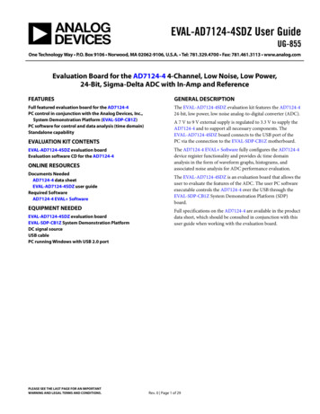
EVAL-AD7124-4SDZ User GuideUG-855One Technology Way P.O. Box 9106 Norwood, MA 02062-9106, U.S.A. Tel: 781.329.4700 Fax: 781.461.3113 www.analog.comEvaluation Board for the AD7124-4 4-Channel, Low Noise, Low Power,24-Bit, Sigma-Delta ADC with In-Amp and ReferenceFEATURESGENERAL DESCRIPTIONFull featured evaluation board for the AD7124-4PC control in conjunction with the Analog Devices, Inc.,System Demonstration Platform (EVAL-SDP-CB1Z)PC software for control and data analysis (time domain)Standalone capabilityThe EVAL-AD7124-4SDZ evaluation kit features the AD7124-424-bit, low power, low noise analog-to-digital converter (ADC).EVALUATION KIT CONTENTSEVAL-AD7124-4SDZ evaluation boardEvaluation software CD for the AD7124-4ONLINE RESOURCESDocuments NeededAD7124-4 data sheetEVAL-AD7124-4SDZ user guideRequired SoftwareAD7124-4 EVAL SoftwareEQUIPMENT NEEDEDEVAL-AD7124-4SDZ evaluation boardEVAL-SDP-CB1Z System Demonstration PlatformDC signal sourceUSB cablePC running Windows with USB 2.0 portPLEASE SEE THE LAST PAGE FOR AN IMPORTANTWARNING AND LEGAL TERMS AND CONDITIONS.A 7 V to 9 V external supply is regulated to 3.3 V to supply theAD7124-4 and to support all necessary components. TheEVAL-AD7124-4SDZ board connects to the USB port of thePC via the connection to the EVAL-SDP-CB1Z motherboard.The AD7124-4 EVAL Software fully configures the AD7124-4device register functionality and provides dc time domainanalysis in the form of waveform graphs, histograms, andassociated noise analysis for ADC performance evaluation.The EVAL-AD7124-4SDZ is an evaluation board that allows theuser to evaluate the features of the ADC. The user PC softwareexecutable controls the AD7124-4 over the USB through theEVAL-SDP-CB1Z System Demonstration Platform (SDP)board.Full specifications on the AD7124-4 are available in the productdata sheet, which should be consulted in conjunction with thisuser guide when working with the evaluation board.Rev. 0 Page 1 of 29
UG-855EVAL-AD7124-4SDZ User GuideTABLE OF CONTENTSFeatures . 1Analog Inputs.7Evaluation Kit Contents . 1Reference Options .8Online Resources . 1Evaluation Board Setup Procedures .8Equipment Needed . 1Evaluation Board Software .9General Description . 1Software Installation Procedures.9Revision History . 2Software Operation . 12EVAL-AD7124-4SDZ Block Diagram . 3Configuration Tab . 12EVAL-AD7124-4SDZ Quick Start Guide . 4Wavefrom Tab . 14Evaluation Board Hardware . 5Histogram Tab . 16Device Description . 5Register Map Tab . 17Hardware Link Options . 5Noise Test—Quick Start Demonstration . 18Power Supplies . 7Evaluation Board Schematics and Artwork . 20Serial Interface . 7Bill of Materials . 27REVISION HISTORY7/15—Revision 0: Initial VersionRev. 0 Page 2 of 29
EVAL-AD7124-4SDZ User GuideUG-855EVAL-AD7124-4SDZ BLOCK DIAGRAM7V TO 9VVINAVDD1.9VLDONCOUTGNDNCENGNDGND2.5V OUTPUTIN57.6kΩNCNCREFOUTBANDGAPREF1.8V OUTPUTGNDOUTGNDENGNDREFIN2( )REFIN2(–)AVSSAVDDGNDINREFIN1(–) IOVDDREFIN1( IOUT/VBIASPGA1PGA224-BITΣ-Δ TERFACEANDCONTROLLOGICX-MUXAIN6/IOUT/VBIAS/REFIN2( STATUSDIAGNOSTICSCOMMUNICATIONSPOWER SUPPLYSIGNAL GPOsDINLEDON-BOARDNOISE TESTAIN0 TO AIN1GND ADP1720 GND3.3V 4-4AVSSDGND13304-001AVSSNOTES1. FOR SIMPLICITY, DECOUPLING NOT SHOWN.Figure 1.Rev. 0 Page 3 of 29
UG-855EVAL-AD7124-4SDZ User GuideEVAL-AD7124-4SDZ QUICK START GUIDETo begin using the evaluation board, do the following:2.3.With the EVAL-SDP-CB1Z board disconnected from theUSB port of the PC, install the AD7124-4 EVAL Software(the software is included on the CD in the evaluation kit,or it can be downloaded from the Analog Devices website).The PC must be restarted after the software installation iscomplete. (For complete software installation instructions,see the Software Installation Procedures section.)Connect the EVAL-SDP-CB1Z board to the EVALAD7124-4SDZ board.Screw the two boards together using the plastic screw andwasher set included in the evaluation board kit to ensurethat the boards are connected firmly together.5.6.Apply an external voltage in the range of 7 V to 9 V to theJ3 or J5 connecter of the EVAL-AD7124-4SDZ board. Thisprovides the power supply for the board.Connect the EVAL-SDP-CB1Z board to the PC using thesupplied USB cable. If you are using Windows XP, youmay need to search for the EVAL-SDP-CB1Z drivers.Choose to automatically search for the drivers for theEVAL-SDP-CB1Z board if prompted by the operatingsystem.From the Programs menu, go to the Analog Devicessubfolder, and click AD7124 Eval to launch the AD7124-4EVAL Software (see the Launching the Software sectionfor further details).13304-0021.4.Figure 2. Hardware Configuration, Setting Up the EVAL-AD7124-4SDZ Evaluation BoardRev. 0 Page 4 of 29
EVAL-AD7124-4SDZ User GuideUG-855EVALUATION BOARD HARDWAREDEVICE DESCRIPTIONThe AD7124-4 is a low power, low noise, complete analog frontend for high precision measurement applications. It contains alow noise, 24-bit, Σ-Δ ADC. It can be configured to have fourdifferential inputs or seven single-ended or pseudo differentialinputs. The on-chip low noise instrumentation amplifier meansthat signals of small amplitude can be interfaced directly to theADC. Other on-chip features include a low drift 2.5 V reference,excitation currents, reference buffers, multiple filter options,and many diagnostic features.Complete specifications for the AD7124-4 are provided in theproduct data sheet, which should be consulted in conjunctionwith this user guide when using the evaluation board. Full detailsabout the EVAL-SDP-CB1Z are available on the Analog Deviceswebsite.HARDWARE LINK OPTIONSTable 1 lists the default link options. By default, the board isconfigured to operate from a wall wart (dc plug) power supplyvia Connector J5. The supply required for the AD7124-4 comesfrom the on-board ADP1720 low dropout regulators (LDOs),which generate their voltage from J5.Table 1. Default Link and Solder Link OptionsLink No.LK1Default OptionALK2BLK3LK4Inserted2.5 VLK5InsertedLK6InsertedSL2ASL3, SL7A, ASL5BAVSS toAGNDDescriptionConnects the AVDD voltage to the power supply sequencer, ADM1185.When AVDD equals 3.3 V, LK1 must be in Position A.When AVDD equals 1.8 V, LK1 must be in Position B.Selects the connector for the external 7 V to 9 V power supply.In Position A, this link selects the external 7 V to 9 V power supply to come from Connector J3.In Position B, this link selects the external 7 V to 9 V power supply to come from Connector J5.Inserting this link connects REFIN( ) to AVSS.Selects the reference source for the ADC.In Position 2.5 V, REFIN1( ) is connected to the external 2.5 V reference (ADR4525).In Position INT REF, REFIN1( ) is connected to the REFOUT pin of the AD7124-4. The internal reference ofthe AD7124-4 can be enabled and applied to the AD7124-4 external to the ADC.This link shorts AIN0 to AIN1. This is useful for performing noise tests on the AD7124-4. The internal biascan be enabled on AIN0 or AIN1 so that AIN0 and AIN1 are at an appropriate voltage for the noise test.LK6 can be used to connect the AIN4 and AIN5 channels to external components such as an externalamplifier. The jumpers in Position A and Position B at LK6 must be opened to include the externalcomponent on the front end.Jumper A and Jumper B of this link can be used to connect the AIN4 and AIN5 channels to externalcomponents such as an external amplifier. For this, the jumpers must be open.Having Jumper A and Jumper B in place connects AIN4 and AIN5 to on-board thermistor used for coldjunction measurements.Sets the voltage applied to the AVDD pin.In Position A, this link sets the voltage applied to the AVDD pin to be a 3.3 V supply from the ADP1720-3.3 (U7)regulator or a 2.5 V supply from the ADP1720 (U4) regulator.In Position B, this link sets the voltage applied to the AVDD pin to be supplied from an external voltagesource via Connector J9.With SL3 and SL7 in Position A, AVDD is supplied with 3.3 V from the ADP1720-3.3 (U7) regulator.With SL3 and SL7 in Position B, AVDD is supplied with 1.8 V from the ADP1720 (U4) regulator.With this link in Position A, the IOVDD supply is provided from an external source via Connector J9.With this link in Position B, the 3.3 V supply is generated by the ADP1720-3.3 (U10) regulator.The evaluation system operates with 3.3 V logic.When these links are inserted, AVSS is tied to AGND. When AVSS is set to 1.8 V, these links must be removed.Rev. 0 Page 5 of 29
UG-855EVAL-AD7124-4SDZ User GuideOn-Board ConnectorsTable 2 provides information about the external connectors on the EVAL-AD7124-4SDZ.Table 2. On-Board 5A6FunctionA 120-pin connector that mates with the EVAL-SDP-CB1Z (controller board).Straight PCB mount SMB/SMA jack for master clock (not inserted). The EVAL-AD7124-4SDZ has the footprint to include anSMA/SMB connector, if an external clock source is being used to provide the master clock to the ADC.Bench top power supply voltage input. Apply 7 V to 9 V and GND (0 V) to this connector to power the evaluation board.Wall wart (dc plug) power supply voltage input. Apply 7 V to 9 V and GND (0 V) to this connector to power the evaluation board.Analog input connector. Connections to AIN0 to AIN5 are available along with REFIN1( ) connections. This connector can beused to connect an RTD to the AD7124-4.Optional external connector, allowing external bench top or alternative supply for AVDD and IOVDD. When split supplies areused, AVSS is supplied externally via J9.Analog input connector. Connections to AIN6 to AIN7 are available along with REFIN1( ) and analog power supply connections.This connector can be used to connect a load cell to the AD7124-4.6-pin connector. Provides an I2C interface to allow the SDP to interface to a digital temperature sensor. This is required if athermocouple is interfaced to the AD7124-4 using Connector A2.7-pin connector that can be used to connect an external amplifier to Channel AIN4/Channel AIN5.7-pin connector that allows connection to the AIN4 and AIN5 pins.Straight PCB mount SMB/SMA jack. The footprint for an SMA/SMB connector is included on the evaluation board to providethe signal to the AIN4 analog input.Straight PCB mount SMB/SMA jack. The footprint for an SMA/SMB connector is included on the evaluation board to providethe signal to the AIN5 analog input.Thermocouple connector. This connector is required if a thermocouple is being interfaced to the evaluation board.Straight PCB mount SMB/SMA jack. The footprint for an SMA/SMB connector is included on the evaluation board to providethe REFIN1( ) signal.Straight PCB mount SMB/SMA jack. The footprint for an SMA/SMB connector is included on the evaluation board to providethe REFIN1( ) signal.Rev. 0 Page 6 of 29
EVAL-AD7124-4SDZ User GuideUG-855POWER SUPPLIESSERIAL INTERFACEThe evaluation board requires that an external power supply—either a bench top supply or a wall wart (dc plug) supply—beapplied to J3 or J5 (see Table 3 for more information). Linearregulators generate the required power supply levels from theapplied VIN rail. The regulators used are the ADP1720-3.3 (U7)and the ADP1720 (U4), which supply 3.3 V and 1.8 V,respectively, to AVDD of the ADC. The 3.3 V ADP1720 (U10)delivers 3.3 V to the IOVDD pin of the AD7124-4.The EVAL-AD7124-4SDZ evaluation board connects via theserial peripheral interface (SPI) to the Blackfin ADSP-BF527on the EVAL-SDP-CB1Z. There are four primary signals: CS,SCLK, DIN, and DOUT/RDY (all are inputs, except forDOUT/RDY, which is an output).When a split power supply is used, the AVSS voltage must beapplied from an external source via Connector J9. AVDD andIOVDD can also be provided via Connector J9. However, the 7 Vto 9 V supply is still required because the on-board reference(ADR4525) is supplied from this power supply.Each supply is decoupled at the point where it enters the boardand again at the point where it connects to each device (see theschematics shown in Figure 26 to Figure 29 to identifydecoupling points).To operate the EVAL-AD7124-4SDZ in standalone mode, theAD7124-4 serial interface lines can be disconnected from the120-pin header by removing the 0 Ω links, R9 through R13. Thetest points can then be used to fly-wire the signals to an alternativedigital capture setup.ANALOG INPUTSThe EVAL-AD7124-4SDZ primary analog inputs can be appliedin two ways: Using J6 and J11, the green screw in terminal connectorsUsing the A0 and A1 SMB/SMA footprints on theevaluation board, which connect to the AIN4 and AIN5analog inputs.The AD7124-4 EVAL Software is set up to analyze dc inputs tothe ADC.Table 3. Required External Power Supply1Power Supply(VIN) Applied ToJ3Voltage Range7 V to 9 VJ57 V to 9 V1FunctionBench top supply to the evaluation board. Supplies LDOs that create the 3.3 V and 1.8 V rails. It alsosupplies the ADR4525 external reference. Ensure that LK2 is set to Position A when the externalpower supply is applied to this connector.Wall wart (dc plug) supply to the evaluation board. Supplies LDOs that create the 3.3 V and 1.8 V rails.It also supplies the ADR4525 external reference. Ensure that LK2 is set to Position B when the externalpower supply is applied to this connector.Only a single supply is required, either J3 or J5. This supply can be selected using LK2.Rev. 0 Page 7 of 29
UG-855EVAL-AD7124-4SDZ User GuideREFERENCE OPTIONSEVALUATION BOARD SETUP PROCEDURESThe EVAL-AD7124-4SDZ includes an external 2.5 V reference(the ADR4525) and an internal 2.5 V reference. The defaultoperation is to use the external reference input, which is set toaccept the 2.5 V ADR4525 on the evaluation board.After following the instructions in the Software InstallationProcedures section, set up the evaluation and SDP boards asdetailed in this section.The reference used for a conversion is selected by choosing thereference in the configuration registers associated with Setup 0to Setup 7. Switch between using the internal reference andexternal reference by accessing the AD7124-4 registers throughthe pop-up windows (discussed in more detail in the followingsections) via the evaluation software. Figure 3 shows how toselect the reference source for Setup 0 to Setup 7. Figure 4shows the ADC CONTROL register setting that enables theinternal reference.The evaluation software and drivers must be installed beforeconnecting the evaluation board and EVAL-SDP-CB1Z board tothe USB port of the PC to ensure that the evaluation system iscorrectly recognized when it is connected to the PC.WarningConfiguring the Evaluation and SDP Boards1.13304-0032.3.13304-004Figure 3. Selecting the Reference SourceFigure 4. Enabling the Internal 2.5 V ReferenceRev. 0 Page 8 of 29Connect the EVAL-SDP-CB1Z board to Connector A orConnector B on the EVAL-AD7124-4SDZ board. Screwthe two boards together using the plastic screw and washerset included in the evaluation board kit to ensure that theboards are connected firmly together.Connect the power supplies to the EVAL-AD7124-4SDZboard. The EVAL-AD7124-4SDZ board, by default, usesthe wall wart (dc plug) supply that accompanies theevaluation kit. Connect this supply to J5 on the EVALAD7124-4SDZ board. (For more information about therequired connections and available options, see the PowerSupplies section.)Connect the EVAL-SDP-CB1Z board to the PC using thesupplied USB cable.
EVAL-AD7124-4SDZ User GuideUG-855EVALUATION BOARD SOFTWARE4.SOFTWARE INSTALLATION PROCEDURESThe EVAL-AD7124-4SDZ evaluation kit includes a CD containingsoftware to be installed on the PC before using the evaluationboard.Select the location to install the software, and then clickNext. (Figure 6 shows the default locations, which aredisplayed when the window opens; you can select anotherlocation by clicking Browse.)There are two procedures in the installation: AD7124-4 EVAL Software installationEVAL-SDP-CB1Z SDP board drivers installationWarningThe evaluation software and drivers must be installed beforeconnecting the evaluation board and EVAL-SDP-CB1Z board tothe USB port of the PC to ensure that the evaluation system iscorrectly recognized when it is connected to the PC.Installing the AD7124-4 EVAL Software3.Figure 6. AD7124-4 EVAL Software Installation:Selecting the Location for Software Installation5.A license agreement appears. Read the agreement, select Iaccept the License Agreement, and click Next.Figure 5. AD7124-4 EVAL Software Installation:Granting Permission for the Program to Make Changes to Your PC13304-0072.With the EVAL-SDP-CB1Z board disconnected from theUSB port of the PC, insert the installation CD into the CDROM drive.Double-click the setup.exe file to begin the evaluation boardsoftware installation. The software installs to the followingdefault location: C:\Program Files\Analog Devices\AD7124 EVAL .A dialog box appears asking for permission to allow theprogram to make changes to your PC. Click Yes.13304-0051.13304-006To install the AD7124-4 EVAL Software, do the following:Figure 7. AD7124-4 EVAL Software Installation:Accepting the License AgreementRev. 0 Page 9 of 29
UG-8556.EVAL-AD7124-4SDZ User GuideInstalling the EVAL-SDP-CB1Z System DemonstrationPlatform Board DriversA summary of the installation displays. Click Next tocontinue.After the installation of the evaluation software is complete, awelcome window displays for the installation of the SDP boarddrivers.With the EVAL-SDP-CB1Z board still disconnected fromthe USB port of the PC, make sure that all otherapplications are closed, and then click Next.13304-0081.Figure 8. AD7124-4 EVAL Software Installation:Reviewing a Summary of the Installation13304-010The message in Figure 9 appears when the installation iscomplete. Click Next.Figure 10. EVAL-SDP-CB1Z Drivers Setup:Beginning the Drivers Installation2.Select the location to install the drivers, and then clickNext.13304-009Figure 9. AD7124-4 EVAL Software Installation:Indicating When the Installation Is Complete13304-0117.Figure 11. EVAL-SDP-CB1Z Drivers Setup:Selecting the Location for Drivers InstallationRev. 0 Page 10 of 29
EVAL-AD7124-4SDZ User Guide3.UG-855Click Install to confirm that you want to install the drivers.Setting Up the System for Data CaptureAfter completing the steps in the Software InstallationProcedures and Evaluation Board Hardware sections, set up thesystem for data capture as follows:13304-0121.2.To complete the drivers installation, click Finish, whichcloses the setup wizard.3.13304-0134.Figure 12. EVAL-SDP-CB1Z Drivers Setup:Granting Permission to Install DriversAllow the Found New Hardware Wizard to run after theEVAL-SDP-CB1Z board is plugged into your PC. (If youare using Windows XP, you may need to search for theEVAL-SDP-CB1Z drivers. Choose to automatically searchfor the drivers for the EVAL-SDP-CB1Z board if promptedby the operating system.)Check that the board is connecting to the PC correctlyusing the Device Manager of the PC.Access the Device Manager as follows:a. Right-click My Computer and then click Manage.b. A dialog box appears asking for permission to allowthe program to make changes to your PC. Click Yes.c. The Computer Management window appears. Fromthe list of System Tools, click Device Manager (seeFigure 15).d. The EVAL-SDP-CB1Z board should appear underADI Development Tools, which indicates that thedriver software is installed and that the board isconnecting to the PC correctly.Before using the evaluation board, you must restart the PC.Figure 15. Device Manager:Checking that the Board Is Connected to the PC Correctly13304-0145.13304-015Figure 13. EVAL-SDP-CB1Z Drivers Setup:Completing the Drivers Setup WizardFigure 14. EVAL-SDP-CB1Z Drivers Setup:Restarting the PCRev. 0 Page 11 of 29
UG-855EVAL-AD7124-4SDZ User GuideLaunching the SoftwareSOFTWARE OPERATIONAfter completing the steps in the Setting Up the System for DataCapture section, launch the AD7124-4 EVAL Software asfollows:Overview of the Main Window2.From the Start menu, click Programs Analog Devices AD7124 Eval AD7124 Eval . The dialog box inFigure 19 appears; select EVAL-AD7124-4SDZ, and themain window of the software then displays as shown inFigure 20.If the AD7124-4 evaluation system is not connected to theUSB port via the EVAL-SDP-CB1Z when the software islaunched, a connectivity error displays (see Figure 16).Connect the evaluation board to the USB port of the PC,wait a few seconds, click Rescan, and then follow the onscreen instructions.13304-0191.The evaluation software supports both the AD7124-4 and theAD7124-8 devices. On running the software, the user selects theevaluation board that is connected to the PC. For the AD7124-4,select EVAL-AD7124-4SDZ from the drop-down list, as shownin Figure 19.13304-016Figure 19. EVAL-AD7124-4SDZ Evaluation Board SelectionFigure 16. Connectivity Error AlertAfter selecting the EVAL-AD7124-4SDZ evaluation board, themain window of the evaluation software displays, as shown inFigure 20. Figure 20 shows the significant control buttons andanalysis indicators of the AD7124-4 EVAL Software. The mainwindow of the AD7124-4 EVAL Software contains four tabs: When the software starts running, it searches for hardwareconnected to the PC. A dialog box indicates when the genericSDP attached to the PC is detected, and then the main windowappears (see Figure 20). Press the RESET button on the SDPboard, as shown in Figure 17.ConfigurationWaveformHistogramRegister MapCONFIGURATION TABThe Configuration tab shows a block diagram of the AD7124-4.It allows the user to set up the ADC, reset the ADC, read thediagnostics to see errors present, as well as configure the devicefor different demo modes. Figure 20 shows the Configurationtab in more detail, and the following sections discuss the differentelements on the Configuration tab of the software window.ADC Reset13304-017Click ADC RESET (Label 2) to perform a software reset of theAD7124-4. There is no hardware reset pin on the AD7124-4. Ahard reset can be performed by removing power to the board.The software reset has the same effect as a hard reset.Selecting External ReferenceFigure 17. SDP Connectivity Board—RESET Button13304-018Pressing the RESET button causes the software to rescan for aconnected SDP board. If found, the message shown in Figure 18displays.Figure 18. Connectivity when SDP and Evaluation Boards are FoundThere are a number of different options that can be used whenselecting the reference to the AD7124-4. Two options are AVddand Refin1( /-) (Label 3). The Refin1( /-). field sets theexternal reference voltage that is connected between REFIN1( )and REFIN1( ). Using the EVAL-AD7124-4SDZ evaluationboard, the AVDD voltage is 3.3 V. Either of these can be used incalculating the results on the Waveform and Histogram tabs.The evaluation board has an external 2.5 V ADR4525 reference,which can be bypassed; if bypassing the ADR4525 on board, besure to change the external reference voltage value in Refin1( /-)to ensure correct calculation of results in the Waveform andHistogram tabs.Rev. 0 Page 12 of 29
EVAL-AD7124-4SDZ User GuideUG-855Tutorial ButtonCONFIG SUMMARYClicking TUTORIAL (Label 4) opens a tutorial on using thesoftware, which provides additional information on using theAD7124-4 EVAL Software.Clicking CONFIG SUMMARY (Label 7) displays the channelconfiguration, information on the individual setups, as well asinformation on any error present. These tabs can be used toquickly check how the ADC channels are configured, as well asany errors that are present.Functional Block DiagramThe functional block diagram of the ADC (Label 5) shows eachof the functional blocks within the ADC. Clicking a configurationbutton on this graph opens the configuration popup window forthat block.Configuration Pop-Up ButtonEach configuration pop-up button (Label 6) opens a differentwindow allowing configuration of the relevant functional block.Demo ModesThe AD7124-4 EVAL Software supports a number of demomodes (Label 8); these demo modes configure the AD7124-4 foreach of the modes shown. A help file is available for each demomode; to access this help file, click the question mark button.Status BarThe status bar (Label 9) displays status updates such as AnalysisCompleted, Reset Completed, and Configuring Demo Modeduring software use, as well as the software version and theBusy indicator.12334756813304-0209Figure 20. Configuration Tab of the AD7124-4 EVAL SoftwareRev. 0 Page 13 of 29
UG-855EVAL-AD7124-4SDZ User GuideWAVEFROM TABChannel SelectionThe Waveform tab graphs the conversions and processes thedata, calculating the p-p noise, rms noise, and resolution (seeFigure 21).The channel selection control (Label 7) chooses which channelsdisplay on the data waveform, and also shows the analog inputsfor the channel labeled next to the on and off controls. Thesecontrols only affect the display of the channels and have noeffect on the channel settings in the ADC register map.Waveform Graph and ControlsThe data waveform graph (Label 1) shows each successivesample of the ADC output. Zoom in on the data using thecontrol toolbar (Label 2) in the graph. Change the scales on thegraph by typing values into the x-axis and y-axis.Analysis ChannelThe Noise Analysis section and histogram graph show theanalysis of the channel selected via the Analysis Channelcontrol (Label 3).SamplesThe Samples numeric control (Label 4) and batch control(Label 5) set the number of samples gathered per batch andwhether a single batch or multiple batches of samples aregathered. This control is unrelated to the ADC mode. The usercan capture a defined sample set or continuously gather batchesof samples. In both cases, the number of samples set in theSamples numeric input dictates the number of samples.SampleClick SAMPLE (Label 6) to start gathering ADC results. Resultsappear in the waveform graph (Label 1).Display Units and Axis ControlsClick the Display Units drop-down list (Label 8) to select whetherthe data graph displays in units of voltages or codes. This controlaffects both the waveform graph and the histogram graph. Theaxis controls can be switched between dynamic and fixed. Whendynamic is selected, the axis automatically adjusts to show theentire range of the ADC results after each batch of sample. Whenfixed is selected, the user can program the axis ranges; the axisranges do not automatically adjust after each batch of sample.CRC Error and Overall ErrorThe CRC Error LED indicator (Label 9) illuminates whena cyclic redundancy check (CRC) error is detected in thecommunications between the software and the AD7124-4. TheCRC functionality on the AD7124-4 is disabled by default andmust be enabled for this indicator to work. The Error PresentLED indicates if an overall error is present in the diagnosticsregister. For this indicator to work, the check for the differentdiagnostic errors must be enabled in the Error EN register.Noise AnalysisThe Noise Analysis section (Label 10) displays the results of thenoise analysis for the selected analysis channel, which includesboth noise and resolution measurements.Rev. 0 Page 14 of 29
EVAL-AD7124-4SDZ User GuideUG-855456713210813304-0219Figure 21. Waveform Tab of the AD7124-4 EVAL SoftwareRev. 0 Page 15 of 29
UG-855EVAL-AD7124-4SDZ User GuideHISTOGRAM TABDisplay Units and Axis ControlsThe Histogram tab generates a histogram using the gatheredsamples and processes the data, calculating the peak-to-peaknoise, rms noise, and resolution (see Figure 22).The data histogram graph (Label 1) shows the number of timeseach sample of the ADC output occurs. Zoom in on the datausing the control toolbar (Label 6) in the graph. Change thescales on the graph by typing values into the x-axis and y-axis.Click the Display Units drop-down list (Label 4) to selectwhether the data graph displays in units of voltages or codes.This c
EVAL-AD7124-4SDZ User Guide UG-855 . see the Software Installation Procedures section.) 2. Connect the EVAL-SDP-CB1Z board to the EVAL-AD7124-4SDZ board. 3. Screw the two boards together using the plastic screw and . This connector can be used to connect a load cell to the : AD7124-4. J12 . 6-pin connector. Provides an I. 2.