Transcription
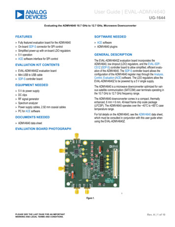
User Guide EVAL-ADMV4640UG-1644Evaluating the ADMV4640 10.7 GHz to 12.7 GHz, Microwave DownconverterFEATURESSOFTWARE NEEDEDFully featured evaluation board for the ADMV4640On-board SDP-S connector for SPI control Simplified power-up with on-board LDO regulators 5 V operation ACE software interface for SPI control GENERAL DESCRIPTIONThe EVAL-ADMV4640Z evaluation board incorporates theADMV4640, low dropout (LDO) regulators, and the EVAL-SDPCS1Z (SDP-S) controller board to allow simplified, efficient evaluation of the ADMV4640. The SDP-S controller board allows theconfiguration of the ADMV4640 register map through the Analysis,Control, Evaluation (ACE) software. The LDO regulators allow theEVAL-ADMV4640Z to be powered by a 5 V single supply.EVALUATION KIT CONTENTSEVAL-ADMV4640Z evaluation board Mini USB to USB cable SDP-S controller board EQUIPMENT NEEDED The ADMV4640 is a microwave downconverter optimized for various satellite communication (SATCOM) user terminals operating inthe 10.7 GHz to 12.7 GHz frequency range.5 V dc power supplyDC clipsRF signal generatorSpectrum analyzerPower supply cables, 2.92 mm coaxial cablesPC for ACE softwareThe ADMV4640 downconverter comes in a compact, thermallyenhanced, 6 mm 6 mm, 40-lead frame chip scale package(LFCSP). The ADMV4640 operates over the 40 C to 85 C casetemperature range.For full details on the ADMV4640, see the ADMV4640 data sheet,which must be consulted in conjunction with this user guide whenusing the EVAL-ADMV4640Z.DOCUMENTS NEEDED ACE softwareADMV4640 pluginsADMV4640 data sheetEVALUATION BOARD PHOTOGRAPHFigure 1.PLEASE SEE THE LAST PAGE FOR AN IMPORTANTWARNING AND LEGAL TERMS AND CONDITIONS.Rev. A 1 of 10
User GuideEVAL-ADMV4640TABLE OF CONTENTSFeatures. 1Evaluation Kit Contents. 1Equipment Needed.1Documents Needed.1Software Needed.1General Description.1Evaluation Board Photograph.1Evaluation Board Hardware.3Evaluation Board Software Quick StartProcedures. 4Installing the ACE Software and ADMV4640Plugins and Drivers. 4Configuring the Board. 4ADMV4640 Block Diagram and Functions. 5Evaluation Board Schematics.7Ordering Information.9Bill of Materials. 9Notes. 10REVISION HISTORY7/2022—Revision A: Initial Version.analog.comRev. A 2 of 10
User GuideEVAL-ADMV4640EVALUATION BOARD HARDWAREThe EVAL-ADMV4640Z comes with an on-board ADMV4640 chip.When evaluating the ADMV4640 device, connect the IF input toan RF signal generator. The EVAL-ADMV4640Z runs on a 5 V dcsupply. Connect the 5 V dc supply to the VCC 5V test point, andthe ground to the GND1 test point.Figure 2 shows the block diagram of the EVAL-ADMV4640Z labbench setup.Figure 2. Lab Bench Setupanalog.comRev. A 3 of 10
User GuideEVAL-ADMV4640EVALUATION BOARD SOFTWARE QUICK START PROCEDURESINSTALLING THE ACE SOFTWARE ANDADMV4640 PLUGINS AND DRIVERSThe EVAL-ADMV4640Z software uses the Analog Devices, Inc.,ACE software. Ensure that the ACE software is installed beforesetting up or using the EVAL-ADMV4640Z. For instructions on howto install and use the ACE software, go to www.analog.com/ACE.If the ACE software has already been installed on the PC, ensure that it is the latest version that is shown on the www.analog.com/ACE page.1. Install the latest version of ACE software. In the ACE Setupwindow, ensure that the SDP Drivers, LRF Drivers, and NET4.8 installations are selected (see Figure 3). Then click Install.3. Connect the 5 V clip lead on the power supply to the redVCC 5V test point on the EVAL-ADMV4640Z, and connectthe GND clip lead on the power supply to the black GND1test point. The power supply current limiting must be set toapproximately 500 mA.4. Open the ACE software. The ADMV4640 Board plugin appears in the Attached Hardware section. Double-click theEVAL-ADMV4640Z plugin. The ADMV4640 Board tab opens(see Figure 5).5. Click off the Poll Device button and double-click theADMV4640 button (see Figure 5).Figure 5. ADMV4640 Board TabFigure 3. Drivers to Install with ACE Software2. Open the ACE software and the EVAL-ADMV4640Z pluginappears (see Figure 4).6. The ADMV4640 block diagram appears (see Figure 6).7. Click the Initialization & Optimization button in theADMV4640 block diagram to initialize the device before operation.Figure 6. ADMV4640 Block Diagram in the ACE SoftwareFigure 4. EVAL-ADMV4640Z Plugin WindowCONFIGURING THE BOARDTo set up the EVAL-ADMV4640Z, take the following steps:1. Connect the SDP-S controller board to the J3 connectors on theEVAL-ADMV4640Z.2. Connect the USB cable to the PC and then to the SDP-Scontroller board.analog.com8. To set up the RF, use the following settings and measure theoutput at the IFOUT port: REF IN port: reference frequency 25 MHz, 3 dBm, and dcblock is needed. RF input: RF frequency 12 GHz, 30 dBm. The gain is at minimum attenuation. Note that the chip temperature is higher than 25 C for the reference frequency andRF frequency conditions and there is part to part variation.The gain may be lower than the typical specifications in theADMV4640 data sheet.Rev. A 4 of 10
User GuideEVAL-ADMV4640ADMV4640 BLOCK DIAGRAM AND FUNCTIONSThe ADMV4640 block diagram user interface with labels is shown in Figure 7, and Table 1 describes the functionality of each block.Figure 7. ADMV4640 Block Diagram with LabelsTable 1. ADMV4640 Block Diagram Label Functions (See Figure 7)LabelFunctionAClick Apply Changes to apply all register values to the device. If Auto Apply is highlighted in the ADMV4640 Board tab, the Apply Changes featurecontinuously runs every few seconds, and does not need to be clicked to apply or read back the block diagram settings.BClick Read All to read back all SPI registers of the device.CClick Rest Chip to reset the ADMV4640 chip.DClick Diff to show registers that are different on the device.EClick Software Defaults to load the software defaults on to the device, and then click Apply Changes.FClick Memory Map Side-By-Side to open the memory map.G1Click the LNA Stage 1 Enable switch (represented by Label G1) to set the LNASTG1 BIAS CONTROL bit (Bit 2, Register 0x100). When the LNAStage 1 Enable switch is highlighted, the LNASTG1 BIAS CONTROL bit is enabled. When the LNA Stage 1 Enable switch is not highlighted, theLNASTG1 BIAS CONTROL bit is disabled.G2Click the LNA Stage 2 Enable switch (represented by Label G2) to set the LNASTG2 BIAS CONTROL bit (Bit 3, Register 0x100). When the LNAStage 2 Enable switch is highlighted, the LNASTG2 BIAS CONTROL bit is enabled. When the LNA Stage 2 Enable switch is not highlighted, theLNASTG2 BIAS CONTROL bit is disabled.HUse the DSA scroll to choose a value, or enter a value in the text box to set the SEL DSA ATTEN bit (Bit[4:0], Register 0x300).IClick the IF Amp Enable switch (represented by Label I) to set the AMPIF BIAS CONTROL bit (Bit 0, Register 0x100). When the IF Amp Enable switch ishighlighted, the AMPIF BIAS CONTROL bit is enabled. When the IF Amp Enable switch is not highlighted, the AMPIF BIAS CONTROL bit is disabled.JClick the LO Amp Enable (represented by Label I) switch to set the AMPLO BIAS CONTROL bit (Bit 1, Register 0x100). When the LO Amp Enable switch ishighlighted, the AMPLO BIAS CONTROL bit is enabled. When the LO Amp Enable switch is not highlighted, the AMPLO BIAS CONTROL bit is disabled.KClick Initialization & Optimization to initialize and lock the synthesizer.L1Enter a value in the VCO Frequency text box to set the VCO frequency. The INT value (Label L2) is calculated based on the VCO Frequency value.Alternatively, change the INT value to calculate the VCO Frequency value.L2Use the INT scroll to choose a value, or enter a value in the text box to set the 16-bit integer value (Register 0x200, Register 0x201) of the PLL. The VCOFrequency value is calculated based on the INT value. Alternatively, change the VCO Frequency value to calculate the INT value.analog.comRev. A 5 of 10
User GuideEVAL-ADMV4640ADMV4640 BLOCK DIAGRAM AND FUNCTIONSTable 1. ADMV4640 Block Diagram Label Functions (See Figure 7)LabelFunctionMEnter a value in the REF IN text box to set the reference frequency.N1Click the Doubler switch to set the DOUBLER EN bit (Bit 3, Register 0x20E). When the Doubler switch is highlighted, the DOUBLER EN bit is enabled. Whenthe Doubler switch is not highlighted, the DOUBLER EN bit is disabled.N2Use the R Divider scroll to choose a value, or enter a value in the text box to change the R divider value (Bit[4:0], Register 0x20C).N3Click the Divide-by-2 switch to set the RDIV2 EN (Bit 0, Register 0x20E). When the Divide-by-2 switch is highlighted, the RDIV2 EN bit is enabled. When theDivide-by-2 switch is not highlighted, the RDIV2 EN bit is disabled.OClick the AMUX switch (represented by Label O) to set the SEL AMUX bit (Bit[2:0], Register 0x301). There are two options for AMUX, AGPIO and temperaturesensor (PTAT).PADC blocks. Click Read from ADC to readback ADC values. See the ADMV4640 data sheet for further details.QClick Proceed to Memory Map to open the ADMV4640 memory map (see Figure 8).RClick the AGPIO switch (represented by Label F) to set the SEL AGPIO bit (Bit 3, Register 0x301). When the AGPIO switch is set to the right, the SEL AGPIObit is disabled and the AGPIO pin is used as data output. When the AGPIO switch is set to the left, the SEL AGPIO bit is enabled and the AGPIO pin is usedas external data input. See the ADMV4640 data sheet for further details.Figure 8. ADMV4640 Memory Map in the ACE Softwareanalog.comRev. A 6 of 10
User GuideEVAL-ADMV4640EVALUATION BOARD SCHEMATICSFigure 9. EVAL-ADMV4640Z Schematic, Page 1analog.comRev. A 7 of 10
User GuideEVAL-ADMV4640EVALUATION BOARD SCHEMATICSFigure 10. EVAL-ADMV4640Z Schematic, Page 2analog.comRev. A 8 of 10
User GuideEVAL-ADMV4640ORDERING INFORMATIONBILL OF MATERIALSTable 2.QtyReference Designators16ManufacturerPart NumberAGPB, GP102, GPIO1, GPIO3, RXON, RX MUTE,Test points, redTP1, VCC 5V, VCC BIAS, VCC CP, VCC IF,VCC LO, VCC REF, VCC SPI, VCC SYN, VCC VCOComponents CorporationTP-104-01-0210C1, C5, C6, C20, C22, C31 to C351000 pF ceramic capacitorsMurataGRM1555C1H102JA012C11, C450.1 µF ceramic capacitorsAmerican Technical Ceramics530L104KT16T1C14390 pF ceramic capacitorMurataGCM1555C1H391JA16D7C3, C7, C8, C15, C17, C25, C3010 pF ceramic capacitorsYageoCC0402JRNP09BN1002C18, C240.47 µF ceramic capacitorsSamsungdCL05A474KA5NNNC1C190.015 µF ceramic capacitorMurataGCM155R71H153JA55D1C23330 pF ceramic capacitorMurataGCM1555C1H331JA16D6C26, C27, C28, C42, C47, C50100 pF ceramic capacitorsTDKC1005NP01H101J050BA7C40, C41, C43, C46, C48, C49, C514.7 µF ceramic capacitorsMurataGRM155R60J475ME87D14C2, C4, C9, C10, C12, C13, C16, C21, C29, C36 toC39, C44Do not installTBD0402TBD04027CPOUT, CSB, MUXOUT, SCLK, SDI, SDO, VTUNETest points, yellowComponents CorporationTP-104-01-041GND1Test point, blackComponents CorporationTP-104-01-004J1, J2, MUX OU, REF INSMA connectorsJohnson142-0701-8511J3120-pin connectorHirose ElectricFX8-120S-SV(21)1P118-pin head connectorSamtec Inc.TSW-109-07-G-D26R1 to R5, R8 to R24, R28, R30, R32, R330 Ω chip resistorsPanasonicERJ-2GE0R00X2R25, R27100 kΩ chip resistorsPanasonicERJ-2RKF1003X2R35, R36100 kΩ chip resistorsVishayCRCW0402100KJNED1R6402 kΩ chip resistorPanasonicERJ-2RKF4020X1R7510 Ω chip resistorYageoRC0402FR-07510RL4R26, R29, R31, R34Do not installTBD0402TBD04021RFIN2.92 mm RF connectorSRI Connector Gage Company25-146-1000-922S1, S2SwitchesEAO09-03-201-021U1ADMV4640Analog DevicesADMV4640BCPZN1U2EEPROMMicrochip Technology24LC32A-I/MS3U3, U4, U5LDO regulatorsAnalog DevicesADM7170ACPZ-3.3-R7analog.comDescriptionRev. A 9 of 10
User GuideEVAL-ADMV4640ORDERING INFORMATIONNOTESESD CautionESD (electrostatic discharge) sensitive device. Charged devices and circuit boards can discharge without detection. Although this product features patented or proprietaryprotection circuitry, damage may occur on devices subjected to high energy ESD. Therefore, proper ESD precautions should be taken to avoid performance degradation or loss offunctionality.Legal Terms and ConditionsBy using the evaluation board discussed herein (together with any tools, components documentation or support materials, the “Evaluation Board”), you are agreeing to be bound by the terms andconditions set forth below (“Agreement”) unless you have purchased the Evaluation Board, in which case the Analog Devices Standard Terms and Conditions of Sale shall govern. Do not use theEvaluation Board until you have read and agreed to the Agreement. Your use of the Evaluation Board shall signify your acceptance of the Agreement. This Agreement is made by and between you(“Customer”) and Analog Devices, Inc. (“ADI”), with its principal place of business at Subject to the terms and conditions of the Agreement, ADI hereby grants to Customer a free, limited, personal,temporary, non-exclusive, non-sublicensable, non-transferable license to use the Evaluation Board FOR EVALUATION PURPOSES ONLY. Customer understands and agrees that the EvaluationBoard is provided for the sole and exclusive purpose referenced above, and agrees not to use the Evaluation Board for any other purpose. Furthermore, the license granted is expressly madesubject to the following additional limitations: Customer shall not (i) rent, lease, display, sell, transfer, assign, sublicense, or distribute the Evaluation Board; and (ii) permit any Third Party to accessthe Evaluation Board. As used herein, the term “Third Party” includes any entity other than ADI, Customer, their employees, affiliates and in-house consultants. The Evaluation Board is NOT soldto Customer; all rights not expressly granted herein, including ownership of the Evaluation Board, are reserved by ADI. CONFIDENTIALITY. This Agreement and the Evaluation Board shall all beconsidered the confidential and proprietary information of ADI. Customer may not disclose or transfer any portion of the Evaluation Board to any other party for any reason. Upon discontinuationof use of the Evaluation Board or termination of this Agreement, Customer agrees to promptly return the Evaluation Board to ADI. ADDITIONAL RESTRICTIONS. Customer may not disassemble,decompile or reverse engineer chips on the Evaluation Board. Customer shall inform ADI of any occurred damages or any modifications or alterations it makes to the Evaluation Board, includingbut not limited to soldering or any other activity that affects the material content of the Evaluation Board. Modifications to the Evaluation Board must comply with applicable law, including butnot limited to the RoHS Directive. TERMINATION. ADI may terminate this Agreement at any time upon giving written notice to Customer. Customer agrees to return to ADI the Evaluation Boardat that time. LIMITATION OF LIABILITY. THE EVALUATION BOARD PROVIDED HEREUNDER IS PROVIDED “AS IS” AND ADI MAKES NO WARRANTIES OR REPRESENTATIONS OF ANYKIND WITH RESPECT TO IT. ADI SPECIFICALLY DISCLAIMS ANY REPRESENTATIONS, ENDORSEMENTS, GUARANTEES, OR WARRANTIES, EXPRESS OR IMPLIED, RELATED TO THEEVALUATION BOARD INCLUDING, BUT NOT LIMITED TO, THE IMPLIED WARRANTY OF MERCHANTABILITY, TITLE, FITNESS FOR A PARTICULAR PURPOSE OR NONINFRINGEMENT OFINTELLECTUAL PROPERTY RIGHTS. IN NO EVENT WILL ADI AND ITS LICENSORS BE LIABLE FOR ANY INCIDENTAL, SPECIAL, INDIRECT, OR CONSEQUENTIAL DAMAGES RESULTINGFROM CUSTOMER’S POSSESSION OR USE OF THE EVALUATION BOARD, INCLUDING BUT NOT LIMITED TO LOST PROFITS, DELAY COSTS, LABOR COSTS OR LOSS OF GOODWILL.ADI’S TOTAL LIABILITY FROM ANY AND ALL CAUSES SHALL BE LIMITED TO THE AMOUNT OF ONE HUNDRED US DOLLARS ( 100.00). EXPORT. Customer agrees that it will not directly orindirectly export the Evaluation Board to another country, and that it will comply with all applicable United States federal laws and regulations relating to exports. GOVERNING LAW. This Agreementshall be governed by and construed in accordance with the substantive laws of the Commonwealth of Massachusetts (excluding conflict of law rules). Any legal action regarding this Agreement willbe heard in the state or federal courts having jurisdiction in Suffolk County, Massachusetts, and Customer hereby submits to the personal jurisdiction and venue of such courts. The United NationsConvention on Contracts for the International Sale of Goods shall not apply to this Agreement and is expressly disclaimed. 2022 Analog Devices, Inc. All rights reserved. Trademarks andregistered trademarks are the property of their respective owners.One Analog Way, Wilmington, MA 01887-2356, U.S.A.Rev. A 10 of 10
EVALUATION BOARD SOFTWARE QUICK START PROCEDURES. analog.com Rev. A 4 of 10. INSTALLING THE ACE SOFTWARE AND ADMV4640 PLUGINS AND DRIVERS The EVAL-ADMV4640Z software uses the Analog Devices, Inc., ACE software. Ensure that the ACE software is installed before setting up or using the EVAL-ADMV4640Z. For instructions on how