Transcription
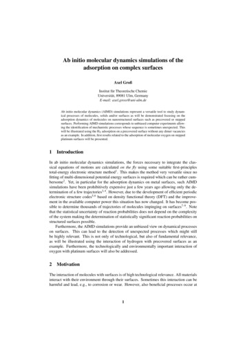
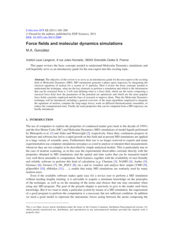
THE JOURNAL OF CHEMICAL PHYSICS 130, 124717 共2009兲Ab initio molecular dynamics simulations of propertiesof a-Al2O3 /vacuum and a-ZrO2 /vacuum vs a-Al2O3 / Ge„100 „2 Ã 1 and a-ZrO2 / Ge„100 „2 Ã 1 interfacesEvgueni A. Chagarova兲 and Andrew C. KummelDepartment of Chemistry and Biochemistry, University of California, San Diego, La Jolla,California 92093, USA共Received 23 April 2008; accepted 8 January 2009; published online 31 March 2009兲The local atomic structural properties of a-Al2O3, a-ZrO2 vacuum/oxide surfaces, anda-Al2O3 / Ge共100兲共2 1兲, a-ZrO2 / Ge共100兲共2 1兲 oxide/semiconductor interfaces were investigatedby density-functional theory 共DFT兲 molecular dynamics 共MD兲 simulations. Realistic a-Al2O3 anda-ZrO2 bulk samples were generated using a hybrid classical-DFT MD approach. The interfaceswere formed by annealing at 700 and 1100 K with subsequent cooling and relaxation. The a-Al2O3and a-ZrO2 vacuum/oxide interfaces have strong oxygen enrichment. The a-Al2O3 / Ge interfacedemonstrates strong chemical selectivity with interface bonding exclusively through Al–O–Gebonds. The a-ZrO2 / Ge interface has roughly equal number of Zr–O–Ge and O–Zr–Ge bonds. Thea-Al2O3 / Ge junction creates a much more polar interface, greater deformation in Ge substrate andinterface intermixing than a-ZrO2 / Ge consistent with experimental measurements. The differencesin semiconductor deformation are consistent with the differences in the relative bulk moduli andangular distribution functions of the two oxides. 2009 American Institute of Physics.关DOI: 10.1063/1.3078035兴I. INTRODUCTIONThe rapid scaling of complementary metal oxide semiconductor 共CMOS兲 technology requires substituting the traditional gate oxide, SiO2, with high-k dielectrics, which canmaintain the same capacitance with much lower leakage current. Amorphous aluminum and zirconium oxides 共a-Al2O3and a-ZrO2兲 are leading candidates for such high- gate oxide materials. Ge is one of a few semiconductors that offersignificantly higher hole mobility than silicon and is beingextensively investigated for p-channel high- metal-oxidesemiconductor field-effect transistor 共MOSFETs兲.1–3Although amorphous oxides are exclusively employed ascommercial gate oxides in MOSFET devices, nearly all reports of density-functional theory 共DFT兲 simulations ofhigh- oxide-semiconductor interfaces are limited to crystalline oxides.4–9 The DFT studies that simulate amorphoushigh-k gate oxides on silicon contain an a-SiO2 interlayer,thereby removing direct high-k amorphous oxidesemiconductor bonds.10 Amorphous oxide-semiconductor interfaces are expected to be superior to crystalline oxidesemiconductor interfaces due to the lack of lattice mismatchthat can induce a high density of interface defects. Despitetheir chemical composition similarity to crystalline phases,amorphous Al2O3 and ZrO2 demonstrate quite different microstructures, coordination distributions, and atomisticchemical environments. Whereas many previously reportedsimulations of oxide-semiconductor interfaces were limitedto the structural relaxation of artificially built systems, in thisa兲Electronic mail: 7/14/ 25.00study MD is applied at finite temperatures to provide theamorphous oxide/semiconductor stacks with enough freedomto evolve to the most realistic state.II. GENERATION OF AMORPHOUS Al2O3 AND ZrO2SAMPLESAmorphous a-Al2O3 and a-ZrO2 samples were generated by applying a hybrid “melt and quench” technique thatemployed classical molecular dynamics 共MD兲 annealing followed by DFT annealing of the classical amorphous sample.Classical MD simulations were performed by a tor共LAMMPS兲,11 expanded by well-tested empirical potentialsfor Al2O3 共Ref. 12兲 and ZrO2.13 All DFT simulations wereperformed with the Vienna ab initio simulation package共VASP兲 共Refs. 14 and 15兲 using projector augmented-wave共PAW兲 pseudopotentials 共PPs兲 共Refs. 16 and 17兲 and relationfunctional.18,19 The choice of PBE functional and PAW PPwas validated by parametrization runs demonstrating goodreproducibility of experimental lattice constants, bulkmoduli, and formation energies for bulk crystalline Al2O3,ZrO2, Al, Zr, and Ge.The a-Al2O3 and a-ZrO2 samples were stoichiometricand consisted of 100 and 96 atoms, respectively. The classical MD generation sequence began with a high-temperatureannealing at 5000 K from a low-density ordered oxide phase共Fig. 1兲. The low-density phase was formed by rescaling theperiodic boundary condition 共PBC兲 box size and oxidesample along every direction by a factor of 1.5 compared tothe box size at classical amorphous density. High-130, 124717-1 2009 American Institute of PhysicsDownloaded 26 May 2009 to 132.239.156.140. Redistribution subject to AIP license or copyright; see http://jcp.aip.org/jcp/copyright.jsp
124717-2J. Chem. Phys. 130, 124717 共2009兲E. A. Chagarov and A. C. KummelFIG. 1. 共Color online兲 Hybrid classical-DFT MD generation sequence ofa-Al2O3 and a-ZrO2 samples. Stages: 共a兲 low- oxide; 共b兲 high-T annealingat low- ; 共c兲 density rescaling 共low normal 兲; 共d兲 high-T annealing atnormal- ; 共e兲 cooling to RT; 共f兲 equilibration at RT; 共g兲 density rescale:classical DFT; 共h兲 annealing below melting T; 共i兲 cooling to 0 K; 共j兲relaxation.temperature annealing at low density provided very goodoxide intermixing and completely erased the original orderedgeometry. After annealing at low density, the sample washomogeneously and instantaneously rescaled back to the normal oxide density and annealed again at 5000 K. 共Themethod of selecting the normal amorphous oxide density isexplained below.兲 Afterwards, the melt was linearly cooled toroom temperature, passing the amorphization point, and thermally equilibrated 共Fig. 1兲.The properties of the classically generated a-Al2O3 anda-ZrO2 samples are sensitive to annealing time at low density and cooling rate. To account for this, these two parameters were varied to give 24 different preparation sequenceswith 24 different final amorphous samples for each sampletype.The amorphous classical samples were quantified viatheir radial-distribution function 共RDF兲 main peak positionsand full widths at half maximum 共FWHM兲, average nearestneighbor numbers, nearest neighbor distributions, and thecalculated neutron scattering static structural factor. TheRDF functions were calculated according to Eq. 共1兲 and averaged over 2001 structure snapshots at 10 fs increments,where N / V is the number density of species , and N is the total number of atoms.20g 共r兲 具n , 共r,r r兲典.4 r2 r共1兲The average nearest neighbor number n 共R兲 关Eq. 共2兲兴 canbe obtained by integrating the corresponding RDF curve upto the cutoff radius R, which is the position of the first minimum after the main RDF peak.n 共R兲 4 B冕Rg 共r兲r2dr.共2兲0The neutron scattering static structure factors 共SN共q兲兲 关Eq.共3兲兴 are obtained from the partial static structure factors共S 共q兲兲 关Eq. 共4兲兴, which are calculated from RDF curvesg 共r兲 关Eq. 共1兲兴, where b is the coherent neutron scatteringlength of species 共bAl 0.3449 10 4 Å, bO 0.5805 10 4 Å兲 共Ref. 20兲 and c 共 兲 N 共 兲 / N is the concentrationof 共 兲 species.20FIG. 2. Nearest neighbor distribution of 共a兲 our classical a-Al2O3 sample vsa larger scale classical sample from Ref. 20. Cutoff radius is 2.2 Å. 共b兲 ourDFT annealed a-ZrO2 sample vs DFT generated sample from Ref. 23. Cutoff radius is 3 Å.SN共q兲 兺 b b 共c c 兲1/2关S 共q兲 共c c 兲1/2兴, 共3兲共兺 b c 兲2S 共q兲 4 共c c 兲1/2冕Rr2关g 共r兲 1兴0 sin共qr兲 sin共 r/R兲dr. r/Rqr共4兲Since the available experimental information on the a-Al2O3and a-ZrO2 microstructures is limited, both experimental andselected simulation data20–26 were used as reference properties. For a-Al2O3, the classically simulated and well-testedamorphous sample was used as the reference state for theclassical MD stage,20 while for a-ZrO2, a DFT generatedsample22–24 was used as the reference state, resulting in theintroduction of a small variation in the sample selection procedure.Of the 24 classical a-Al2O3 samples, the most realisticsample, as quantified by RDF main peak positions andFWHMs, average nearest neighbor numbers, nearest neighbor distributions, and the calculated neutron scattering staticstructural factor, was the sample that had been classicallyprepared by annealing at 5000 K for 350 ps at low共 0.9 g / cm3兲 density, instantaneously rescaled with thePBC box to the normal density of 3.20 g / cm3 共see commentbelow兲 and annealed for 400 ps, linearly cooled to RT forDownloaded 26 May 2009 to 132.239.156.140. Redistribution subject to AIP license or copyright; see http://jcp.aip.org/jcp/copyright.jsp
124717-3J. Chem. Phys. 130, 124717 共2009兲Ab initio molecular dynamics simulationsFIG. 3. 共Color online兲 RDF curves for the a-Al2O3 sample generated byclassical MD.100 ps and thermally equilibrated at RT for 100 ps 共Fig. 1兲.During Al2O3 high-T 共5000 K兲 annealing at low density, thefinal average atom displacement was 7.6 Å or 70% of thesmallest PBC lattice vector 共11.0 Å兲. During the subsequentnormal density high-T Al2O3 annealing, the average atomdisplacement was 5.1 Å or 65% of the smallest lattice vector 共7.8 Å兲. The total velocity integration over time indicatedan absence of oxide correlated macroscopic motion throughPBC boundaries. The high values of average atomic displacement during high-T annealing phases are consistentwith a high degree of melt intermixing. Note that these values may be a slight underestimate of the real atom displacements since some atoms pass the whole PBC box. Althoughsample vaporization can happen during low-density high-Tannealing phase, vaporization provides good sample intermixing and has no significant effect on final sample properties; the final sample properties are mainly affected by theamorphization processes during cooling phase.Amorphous Al2O3 can be stable over a wide range ofdensities. Experimental measurements report stable amorphous Al2O3 structures with a 3.05– 3.40 g / cm3 densityrange,27,28 while classical and DFT computer simulationsdemonstrate successful generation at 3.0– 3.3 g / cm3.20,29,30The classical density of the a-Al2O3 sample in this study waschosen to be consistent with previous classical simulations ofa-Al2O3 that correlated well with experimentalproperties.20,21 The selected a-Al2O3 classical sample is ingood agreement with MD simulated nearest neighbor distributions, RDF main peak positions 共Figs. 2 and 3, Table I兲and neutron scattering static structure factors reported byGutierrez and Johansson20 as well as to experimentally measured bond lengths, and neutron scattering static structurefactors.21 Our simulated sample contains moderate deviations in the average coordination numbers when compared toFIG. 4. 共Color online兲 共a兲 a-Al2O3 and 共b兲 a-ZrO2 samples after DFT annealing. Al dark blue, Zr: light blue, O: red.the reference samples20,21 since our sample has only 100 atoms whereas the sample in Ref. 20 consisted of 1800 atomsand the sample from Ref. 21 was macroscopic. Furthermore,the experimental coordination distribution and average coordination numbers reported earlier were obtained from experimental x-ray and neutron diffraction curves by the reverseMonte Carlo technique, which could potentially introducesome ambiguity and statistical error in the obtained values.21To match the DFT amorphous density, the most realisticclassical a-Al2O3 sample was homogeneously rescaled fromthe classical 共3.20 g / cm3兲 to the DFT density 共3.26 g / cm3兲resulting in a sample size of 11.6 11.6 7.8 Å. Therescaled sample was then DFT annealed at 1500 K for1000 fs with a 1.0 fs time step, cooled to 0 K for 200 fs, andrelaxed at fixed volume to a value below the specified0.01 eV/ Å force tolerance level 关Figs. 1 and 4共a兲兴. The stresstensor components of the DFT annealed amorphous samplewere analyzed to verify the absence of any significant internal hydrostatic pressure. The goal of DFT annealing is toprovide adjustment to the more accurate DFT force fieldwithout complete melting the initial rescaled classical sampleused as a first approximation. Since the DFT annealing wasperformed at constant volume at the amorphous density共which is considerably lower than the crystalline density兲and for a limited time 共 1 ps兲, recrystallization processeswere prevented as verified by the final RDF curves beingconsistent with an amorphous state. To determine the ratio ofclassical and DFT density, a separate classical a-Al2O3sample was DFT annealed using the same procedure and,subsequently, relaxed at variable volume. The electronicstructure analysis of the DFT annealed and relaxed a-Al2O3bulk sample indicates a bandgap of 3.80 eV that is free fromany defect states, agreeing well with a previously reportedDFT bandgap of 3.77 eV.29 Due to the wider coordinationdistribution in amorphous samples compared to crystallineTABLE I. RDF peak maxima and average nearest neighbor numbers for our classical MD a-Al2O3 sample vsa large-scale reference classical MD sample 共Ref. 20兲 and experimental data 共Ref. 21兲.Our sampleAl–OO–OAl–AlSimulationsExperimentRDFn RDFn RDFn .82.83.24.18.56.0Downloaded 26 May 2009 to 132.239.156.140. Redistribution subject to AIP license or copyright; see http://jcp.aip.org/jcp/copyright.jsp
124717-4E. A. Chagarov and A. C. Kummelones, our amorphous sample bandgap is lower than the DFTcalculated crystalline Al2O3 bandgap 共 6.0 eV兲.29,31 The angular distribution function 共ADF兲 of our sample demonstrates strong correlation to the previously reported values.20Gutierrez and Johansson reported O–Al–O peak at 104 versus 102 for our sample.20 The Al–O–Al ADF presented inRef. 20 demonstrates peak at 120 versus 122 for oursample. The small deviation of our angular distribution datafrom Ref. 20 can be explained by the fact that Ref. 20 reportsupon a classically annealed sample, while our sample wasproduced by sequential classical and DFT annealing, whichintroduced the more accurate DFT force field at the end ofthe simulations.The classical models of a-ZrO2 oxide were prepared in abatch of 24 different samples with a density of 4.71 g / cm3.This model follows the same general procedure used for thea-Al2O3 system but with different annealing/cooling times共Fig. 1兲. The classical amorphous density was calculatedfrom the DFT amorphous density 共see comment below兲 andclassical-to-DFT density correction ratio. Since the amountof experimental microstructure data on a-ZrO2 is limited andoften varies with the sample preparation technique, both published DFT simulations as well as experimental measurements were used as reference sample properties.22–26,32,33 Themost realistic classical a-ZrO2 sample was generated by annealing at 5000 K at low density 共 1.4 g / cm3兲 for 500 ps,instantaneously rescaling the PBC box to the normal classical density of 4.71 g / cm3, annealing for 500 ps, linearlycooling to RT for 100 ps, and thermally equilibrating at RTfor 100 ps. During ZrO2 high-T 共5000 K兲 annealing at lowdensity, the final average atom displacement was 7.9 Å or 53% of the smallest PBC lattice vector. At the normal density high-T ZrO2 annealing, the average atom displacementwas 5.46 Å or 54% of the smallest lattice vector. The highvalues of average atomic displacement during high-T annealing phases are consistent with a high degree of the meltintermixing. Note, these values may be a slight underestimate of the real atom displacement since some atoms passthe whole PBC box.Since previous DFT simulations reported realistic amorphous a-ZrO2 structures for a density range between 4.86and 5.32 g / cm3,22,23 a relatively low DFT sample densityvalue 共4.90 g / cm3兲 was selected to minimize the risk ofsample recrystallization during DFT annealing and cooling.The sizes of the DFT a-ZrO2 samples were 11.58 11.58 10.0 Å, equivalent to the Ge共100兲 slab surfacearea. Since the a-ZrO2 reference sample microstructure wasDFT generated, the three classical samples demonstrating theleast deviation of nearest neighbor distribution from the reference sample were selected, rescaled to a DFT density of4.90 g / cm3, and DFT annealed at 2800 K for 1000 fs,cooled to 0 K for 200 fs and relaxed at fixed volume to a0.01 eV/ Å force tolerance level 共Fig. 1兲.23 The DFT amorphous oxide annealing was performed at fixed low amorphous density for a limited time interval 共 1 ps兲 effectivelypreventing sample recrystallization as proven by the RDFcurves and nearest neighbor distribution. These threesamples were analyzed to determine their final nearest neighbor distributions; the closest match to the reference sampleJ. Chem. Phys. 130, 124717 共2009兲was selected and thoroughly tested 关Figs. 2共b兲 and 4共b兲兴. Inaddition to the good agreement between the nearest neighbordistributions of the selected sample and the reference one23关Fig. 2共b兲兴, the selected sample also indicates a good correlation of its RDFs with that of the reference sample. TheZr–O RDF main peak is located at 2.1 Å with a Zr–O lengthdistribution primarily in the 2.0– 2.3 Å interval versus previously reported intervals of 2.04– 2.25 Å.22–24 The Zr–Zr andO–O RDF main peaks are located at 3.5 and 2.8 Å, respectively. The stress tensor components of the selected DFTannealed a-ZrO2 amorphous sample were analyzed to verifythe absence of significant internal hydrostatic pressure.The DOS and bandgap analysis is an important test sinceit can screen out defective samples with states in the bandgap. The selected a-ZrO2 sample has a bandgap of 2.7 eVfree from defect states in comparison with previously reported amorphous 3.2 eV 共DFT, 5.32 g / cm3兲, 3.4 eV共DFT, 4.86 g / cm3兲 and experimental 4.7 eV 共Refs.23–26兲 values. This discrepancy with experiment is mainlydue to the standard DFT bandgap underestimation caused byan inadequate description of the DFT exchange interaction.The DFT sample in Ref. 24 with the 3.2 eV bandgap wasprepared at a different density 共5.32 g / cm3 versus our4.90 g / cm3兲, using a different generation technique 共ARTversus our DFT MD兲, and with a different code 关LCAO code共SIESTA兲 versus a plane-wave code 共VASP兲兴. The DFT samplein Ref. 23 with a bandgap of 3.4 eV was generated by DFTMD at a time scale that was 55 times shorter than ourcombined classical-DFT time scale of 1201 ps and had acooling rate approximately times steeper than in our runs.The problem of all MD atomistic simulations is that the computationally affordable cooling rate is much higher than thecooling rate in real experiments. Performing the amorphization at too high cooling rate can lead to a less realisticsample, since too fast cooling can freeze the liquid state instead of providing the system with enough time for properamorphization. Therefore, decreasing of the simulated cooling rate actually makes amorphization simulations more realistic. The significantly longer time scale and lower coolingrate used in our runs lead to better intermixing and moreextensive and realistic amorphization. Since passage fromthe crystalline to amorphous phase typically decreases thebandgap, the smaller value of our sample bandgap can beattributed to our longer run time scale and lower coolingrate.29III. OXIDE/Ge INTERFACIAL BONDING SIMULATIONSThe 64-atom Ge共100兲共2 1兲 substrate was built from a2 2 2 Ge supercell with the DFT optimized lattice constant. The bottom three layers were fixed in the bulk positions and saturated by H atoms. The rest of the slab wasrelaxed below the 0.01 eV/ Å force tolerance level to formthe Ge共100兲共2 1兲 surface reconstruction with an 11.58 11.58 10.4 Å slab size. To satisfy periodic boundaryconditions, the DFT relaxed oxide sample size perfectlymatches the DFT relaxed Ge surface area.The DFT annealed oxide samples 共a-Al2O3 and a-ZrO2兲were cleaved along the X-Y plane parallel to the oxide-Downloaded 26 May 2009 to 132.239.156.140. Redistribution subject to AIP license or copyright; see http://jcp.aip.org/jcp/copyright.jsp
124717-5Ab initio molecular dynamics simulationsFIG. 5. 共Color online兲 General DFT preparation sequence for a-Al2O3 / Geand a-ZrO2 / Ge interfaces. Stages: 共a兲 initial relaxation 共 30 steps兲; 共b兲annealing 共 1000 fs兲; 共c兲 cooling to 0 K 共 200 fs兲; 共d兲 final relaxation共 500– 1500 steps兲; 共e兲 final relaxation at extended K-point mesh 共 50steps兲.semiconductor interface and periodic boundary conditionswere truncated by adding 12 Å of vacuum over thesamples. The technique of cleaving an oxide sample beforebonding is similar to the approach of Broqvist et al.10,34 Thecleavage planes were chosen to provide a roughly equalnumber of metal and oxygen atoms at the bottom surface.Each cleaved amorphous oxide slab was placed on the relaxed Ge共100兲共2 1兲 surface at an interfacial distance so thatthe initial Al–Ge or Zr–Ge pair lengths were equal to approximately 0.5–0.75 of their empirical equilibrium distance.The oxide sample was not relaxed after surface cleavageprior to stacking on Ge in order to provide a chemicallyreactive surface with dangling bonds for contact with Ge.Conversely, the upper surface of the oxide was passivated byH atoms having 12 Å of vacuum to avoid spurious interactions through periodic boundary conditions. In contrast toother published DFT-MD oxide/semiconductor studies, weuse models with one oxide/semiconductor interface and avacuum layer since the supercell model with two oxide/semiconductor interfaces and no vacuum might unphysicallyrestrict atomic migration to/from the oxide/semiconductorinterface in the thin oxide film 共 10 Å兲.10,34 In addition, thepresence of a vacuum layer over the oxide allows for thecomplete relaxation of the interfacial oxide-semiconductorheight and any possible residual stresses in the amorphoussample induced by bonding to the semiconductor. To compensate for spurious electric fields induced by PBC for thistype of system, a dipole correction was applied.14,15,35After oxide/semiconductor stacking, the whole Ge slabwas fixed in space while the oxide was partially relaxed for 20– 30 conjugate-gradient 共CG兲 relaxation steps. The duration of this initial relaxation was systematically determinedby performing longer 共 150 CG steps兲 relaxation run whichshowed that 20– 30 CG steps were sufficient to reach theoptimal interface height, thereby releasing initial artificialstresses and allowing the oxide to conform to the nonplanarreconstructed Ge共100兲共2 1兲 topography. After the 20– 30CG steps of initial partial relaxation with frozen Ge, the Geatoms were unfixed except for the three bottom layers andthe whole system was annealed at 700 or 1100 K for 1000 fswith 1.0 fs time steps, cooled to 0 K for 200 fs, and finallyrelaxed below a 0.05 eV/ Å force tolerance level 共Fig. 5兲.The system was annealed at two different temperatures 共700and 1100 K兲 to investigate the effects of annealing tempera-J. Chem. Phys. 130, 124717 共2009兲ture on interface properties and to evaluate possible influences of increased annealing time scale, which can be estimated by the faster kinetics at high temperature. Since thePBC box is large and the system runs included 200 atomsand 2500 CG/MD steps, the initial relaxation, annealing,cooling, and final relaxation were performed with a 2K-point irreducible mesh to obtain acceptable computationalefficiency. After the final relaxation, the K-point set was expanded to a 3 3 1 mesh, and the system was tuned byanother relaxation run. Although expanding the K-point sethad no visible effect on the system geometry and requiredonly 30– 50 CG steps to relax below the 0.05 eV/ Å forcetolerance level, it could improve the electronic structure. Theprocess of annealing, cooling, and relaxing the oxide/semiconductor stack provides unique microscopic insightinto the interface evolution and the final microstructure共Figs. 6 and 7兲.IV. VACUUM/OXIDE a-Al2O3 AND a-ZrO2 INTERFACESThe amorphous bulk samples 共Fig. 4兲 were used to generate vacuum/oxide a-Al2O3 and a-ZrO2 interfaces 共Fig. 8兲to provide a comparison to the oxide/semiconductor interfaces. For the bulk amorphous samples, the periodic boundary condition box was extended in the Z-direction by adding 15.0 Å of vacuum space thereby creating two unrelaxedsurfaces. The bulk cleavage plane was chosen to provide aroughly equal number of metal and oxygen atoms on eachcleaved surface. The cleaved a-Al2O3 slab was annealed at1500 K for 1000 fs with 1.0 fs time steps, cooled to 0 K for200 fs, and relaxed to the ground state with a 0.05 eV/ Åforce tolerance level. The cleaved a-ZrO2 slab was annealed,cooled, and relaxed similarly except the annealing temperature was 2800 K 共Fig. 8兲. The experimental melting temperature for Al2O3 is 2326 K, however, since melting temperatures in DFT simulations can differ from experimental onesand since a reliable DFT melting temperature for a-Al2O3 isnot available, an overcautious temperature of 1500 K wasused for DFT MD annealing of the a-Al2O3 sample.36 Thea-ZrO2 was previously thoroughly investigated by DFT MD,reporting signs of disorder at 3000 K, and definite melting at4000 K;22–24 therefore an annealing temperature of 2800 Kcould be used for a-ZrO2 even though it was higher than thea-Al2O3 DFT annealing temperature employed in this study.After annealing and relaxation, the slabs were analyzed toverify their amorphous state. Although real oxide-vacuuminterfaces are likely to be OH terminated, the oxide-vacuuminterfaces were not terminated with OH to facilitate understanding the influence of semiconductor bonding to the oxidesurface compared to the surface of the same oxide withoutany termination. The current research was intended to investigate and compare fundamental properties of a-Al2O3 / Ge,a-ZrO2 / Ge, and vacuum/a-Al2O3, vacuum/a-ZrO2 interfaces, which have not been theoretically investigated before,in the absence of interface absorbates such as OH or N.Downloaded 26 May 2009 to 132.239.156.140. Redistribution subject to AIP license or copyright; see http://jcp.aip.org/jcp/copyright.jsp
124717-6E. A. Chagarov and A. C. KummelJ. Chem. Phys. 130, 124717 共2009兲FIG. 6. 共Color兲 a-Al2O3 / Ge共100兲共2 1兲 interfaces annealed at 700 and 1100 K. Al: blue, O: red, Ge: green, H: white. Note that after final relaxation theinterfaces are dominated by O–Ge bonds and the Ge substrate is distorted.V. RESULTS AND DISCUSSIONIt is very informative to compare structural properties ofa-Al2O3 / Ge and a-ZrO2 / Ge interfaces with vacuum/oxidea-Al2O3 and a-ZrO2 ones.A. Chemical segregation and interfacial dipoles at theoxide/semiconductor and vacuum/oxide interfacesThe DFT annealing of vacuum/a-Al2O3 surfaces revealsa pronounced interface chemical segregation with Al atomsmigrating into the bulk and O atoms migrating to the surfaceto create O surface capping 关Fig. 8共a兲兴. This phenomenon ofoxygen enrichment of oxide/vacuum interfaces was previously reported for classical MD simulations of thevacuum/a-Al2O3 interfaces,30 and by first-principle simulations of the 共0001兲 interfaces of - and 共001兲 interfaces ofcrystalline -alumina with vacuum.37,38 The surface segregation at the vacuum/a-Al2O3 interface can be explained by thedifferent geometries of O and Al bonds. In a-Al2O3, bulk Alatoms predominantly have four or five nearest neighbors共Fig. 2兲. The Al atom located at the oxide-vacuum interfacewould likely have a lower number of neighbors thereby increasing the total energy of the system. The O atoms predominantly have only two or three neighbors in the a-Al2O3bulk 共Fig. 2兲; therefore, they will more likely accommodatebonding at the vacuum/oxide interface without significantlychanging the total energy.The a-Al2O3 / Ge interfaces annealed at 700 and 1100 Kdemonstrate very similar interface oxygen enrichment compared to the vacuum/a-Al2O3 interface 共Fig. 6兲. Fora-Al2O3 / Ge interfaces, oxygen atoms migrate to the semiconductor interface and Al atoms migrate into the bulk oxideresulting in interfacial bonding exclusively through Al–O–Ge bonds with no or very few O–Al–Ge bonds.39 ThisO-rich bonding is present even during the high-temperatureannealing stage 关Figs. 6 and 9共a兲兴. The interface segregationoccurs during the first 100 fs 共10% of the whole annealingtime兲, indicating the DFT time scale used is sufficient toobserve this phenomenon 共Fig. 6兲. Increasing the interfacialannealing temperature from 700 to 1100 K has no effect onthis interface chemical migration.Interfacial bonding exclusively through Al–O–Ge bondscan result in strong interface polarity; this is not a desiredcharacteristic as significant charge transfer has a negativeimpact on device performance. To verify and quantify thiseffect, a Bader charge analysis was performed.40,41 TheBader charge analysis indicates that for the a-Al2O3 / Ge interfaces annealed at 700 and 1100 K, the Ge atoms bondedto O lose, on average, about 0.7–1.0 兩e兩 of atomic chargeDownloaded 26 May 2009 to 132.239.156.140. Redistribution subject to AIP license or copyright; see http://jcp.aip.org/jcp/copyright.jsp
124717-7Ab initio molecular dynamics simulationsJ. Chem. Phys. 130, 124717 共2009兲FIG. 7. 共Color兲 a-ZrO2 / Ge共100兲共2 1兲 interfaces annealed at 700 and 1100 K. Zr: light blue, O: red, Ge: green, H: white. Note that after final relaxation,there are both Zr–O–Ge and O–Zr–Ge bonds and the Ge substrate has low distortion.共Fig. 6兲. To investigate the total charge transfer from the Gesubstrate into the a-Al2O3 bulk through the semiconductor/oxide interface, the total Bader atomic charge was summedup over all Ge atoms and bottom passivating H’s in thea-Al2O3 / Ge system and compared to the same total chargesummed up over the clean vacuum/semiconductor Ge共100兲 共2 1兲 slab with bottom passivating H atoms. This totalcharge transfer analysis indicates that the 700 K annealedinterface depletes the Ge substrate by 9.23 兩e兩 of charge corresponding to a
Ab initio molecular dynamics simulations of properties . employed classical molecular dynamics MD annealing fol-lowed by DFT annealing of the classical amorphous sample. Atomic/Molecular Massively Parallel Simulator LAMMPS ,11 expanded by well-tested empirical potentials for Al 2O 3 Ref. 12 and ZrO 2. 13 All DFT simulations were performed with the Vienna ab initio simulation package VASP .