Transcription
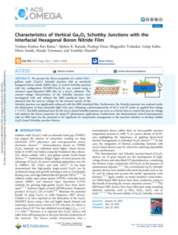
istics of Vertical Ga2O3 Schottky Junctions with theInterfacial Hexagonal Boron Nitride FilmVenkata Krishna Rao Rama,* Ajinkya K. Ranade, Pradeep Desai, Bhagyashri Todankar, Golap Kalita,Hiroo Suzuki, Masaki Tanemura, and Yasuhiko Hayashi*Downloaded via OKAYAMA UNIV on August 8, 2022 at 02:11:00 (UTC).See https://pubs.acs.org/sharingguidelines for options on how to legitimately share published articles.Cite This: ACS Omega 2022, 7, 26021 26028ACCESSRead OnlineMetrics & MoreArticle RecommendationsABSTRACT: We present the device properties of a nickel (Ni) gallium oxide (Ga2O3) Schottky junction with an interfacialhexagonal boron nitride (hBN) layer. A vertical Schottky junctionwith the configuration Ni/hBN/Ga2O3/In was created using achemical vapor-deposited hBN film on a Ga2O3 substrate. Thecurrent voltage characteristics of the Schottky junction wereinvestigated with and without the hBN interfacial layer. Weobserved that the turn-on voltage for the forward current of theSchottky junction was significantly enhanced with the hBN interfacial film. Furthermore, the Schottky junction was analyzed underthe illumination of deep ultraviolet light (254 nm), obtaining a photoresponsivity of 95.11 mA/W under an applied bias voltage( 7.2 V). The hBN interfacial layer for the Ga2O3-based Schottky junction can serve as a barrier layer to control the turn-on voltageand optimize the device properties for deep-UV photosensor applications. Furthermore, the demonstrated vertical heterojunctionwith an hBN layer has the potential to be significant for temperature management at the junction interface to develop reliableGa2O3-based Schottky junction devices. INTRODUCTIONGallium oxide (Ga2O3) with an ultrawide band gap (UWBG)has piqued the interest of researchers working on deepultraviolet (UV) photonics and next-generation powerelectronic devices.1 5 Semiconductors based on UWBGGa2O3 materials can withstand much higher critical electricfields (6 8 MV/cm) before avalanche breakdown than silicon(Si), silicon carbide- (SiC), and gallium nitride (GaN)-baseddevices.1,6,7 Furthermore, Baliga’s figure of merit presents theadvantage of Ga2O3 for power switching applications over theSi (3000 ), SiC (10 ), and GaN (4 ).8,9 It has beendemonstrated that high-quality single-crystal Ga2O3 can besynthesized using melt growth techniques such as Czochralski,floating zone, and edge-defined film-fed growth (EFG).10 15 Inaddition, halide vapor phase epitaxy (HVPE), molecular beamepitaxy (MBE), and chemical vapor deposition (CVD)methods for growing high-quality Ga2O3 have been developed.16 25 Johnson’s figure of merit (JFOM/power frequencyproduct) of Ga2O3 (3 of GaN)26,27 illustrates the potentialbenefit of using Ga2O3 in radio frequency (RF) devices.Chabak et al. have reported on the fabrication of the Ga2O3MOSFET device using a thin and highly doped channel andachieving a drain-source current of 275 mA/mm at a drain tosource bias of 10 V for that exhibited record-high f t/f max 5.1/17.1 GHz.28 However, it is expected that Ga2O3 devices willsuffer from self-heating due to the poor thermal conductivity ofthe material. The device model demonstrates that a 2022 The Authors. Published byAmerican Chemical Societyhomoepitaxial device suffers from an unacceptable junctiontemperature increase to 1500 C at a power density of 10 W/mm, highlighting the importance of applying device-levelthermal managements to individual Ga2O3 devices.29,30 In thiscase, the integration of thermal conducting materials withGa2O3-based devices may be critical for achieving dependabledevice performance.The heterojunction and Schottky junction-based β-Ga2O3devices are of great interest for the development of highvoltage devices and solar-blind UV photodetectors, consideringthe intrinsic n-type conductivity of β-Ga2O3 in the presence ofunintentional dopants.25 31 The conventional Ga2O3 Schottkyjunction devices were studied with metal electrodes such as Au,Pt, and Ni, taking into account the metals’ appropriate workfunction.32,33 Again, studies on metal insulator semiconductor (MIS)-based SBD devices have been conducted, owing tothe benefit of lowering the reverse saturation current.34 36 TheMIS-based SBD devices have been fabricated using insulatingdielectric materials, such as SiO2, Si3N4, Al2O3, and soforth.35 37,40 The thermal stability of Ga2O3 Schottky contactsReceived: January 25, 2022Accepted: May 18, 2022Published: July 22, CS Omega 2022, 7, 26021 26028
ACS re 1. (a) Schematic diagram of the APCVD process for synthesis of the hBN film on Cu foil. (b) Transfer process of the CVD-synthesizedhBN film for the fabrication of the Ni/hBN/β-Ga2O3/In heterojunction Schottky diode.Figure 2. (a) Cross-sectional schematic diagram of the hBN and β-Ga2O3 heterostructure. (b) XRD pattern of the free-standing β-Ga2O3 substrate.(c) SEM image of the hBN film on the β-Ga2O3 substrate. (d) Raman spectra of the β-Ga2O3 sample.is also an important aspect, for which materials with highmelting temperatures and low reactivity with Ga2O3 are ofsignificant interest.37 Furthermore, controlling near-surface iondamage during sputtering deposition of a barrier layer/insulating dielectric7,40 is required. In this case, the CVDsynthesized chemically inert insulating hBN layer will besignificant with much higher in-plane thermal conductivity foruse in Ga2O3-based Schottky junctions.38,39Previously, we have demonstrated the integration of highlyconducting graphene and copper iodide (γ-CuI) films with theβ-Ga2O3 substrate for the fabrication of deep-UV photoresponsive devices.41,42 The fabrication of quasi-two-dimensional metal insulator semiconductor field-effect transistorswas demonstrated by the mechanical transfer process of hBNand nanothin flakes of β-Ga2O3.43 In contrast to previousreports, we show how to make a vertical Ni/β-Ga2O3 Schottkyjunction with and without the hBN interfacial layer. TheUWBG heterostructure of hBN and β-Ga2O3 can be significantdue to the complementing electronic, chemical, and thermalproperties of the materials. The following sections go over thespecifics of hBN integration with the free-standing β-Ga2O3substrate and the fabrication of a vertical Schottky junction.We discovered that the hBN interfacial film can be used tocontrol the device’s turn-on voltage and current density. EXPERIMENTAL SECTIONThe hBN film was synthesized on recrystallized Cu (111) foilby the atmospheric pressure CVD (APCVD) as reportedpreviously by the research group (Figure 1a).44 46For this experiment, ammonia borane (10 mg) is used as aprecursor and placed atop a magnetic boat, which was placedinside the tube about 20 cm away from the furnace to avoidprecursor loss before the deposition step. The furnace was setat a high temperature of 1050 C for the growth of the hBNfilm on the Cu surface. During the deposition step, the gas flowinto the chamber was changed by the addition of argon gaswith a flow rate of 98 sccm, and the flow rate of hydrogen gaswas reduced to 2 sccm, and the mixed gas flow was 98:2 of Ar/H2. To achieve vaporization of ammonia borane, the precursoris brought close to the furnace using a magnet at 3 cm awayfrom the furnace, as shown in the schematic diagram (Figure1a). The deposition step was set for 40 min, allowing for S Omega 2022, 7, 26021 26028
ACS re 3. XPS spectra for the fabricated hBN/β-Ga2O3 heterostructure sample. (a) B 1s spectra with a peak center at around 192.8 eV, (b) N 1sspectra with a peak center at 400.1 eV, (c) Ga 3d spectra with a peak center at 22.3 eV, and (d) Ga 2p3/2 and Ga 2p1/2 peaks with peak centers at1119.4 and 1146.0 eV, respectively.Figure 4. J V characteristic of the Ni/β-Ga2O3/In Schottky junction: (a) J V characteristic for the voltage range of 2 to 2 V (inset shows aschematic diagram of the fabricated device) and (b) log plot of the J V curve. (c) J V characteristics of the forward and reverse sweep for thevoltage range of 2 to 2 V. (d) J V curve under dark and deep-UV illumination (254 nm).formation of an hBN layer on a Cu (111) substrate. Finally, thecooling step was completed by simultaneously switching theH2 gas flow, partially opening the furnace, and moving theprecursor approximately 20 cm away from the furnace to avoida secondary deposition. After the reaction chamber was cooledto room temperature, the hBN-grown Cu foil was removed andsubjected to a wet transfer process described in the previousreports.44 An hBN/β-Ga2O3 stack was obtained by transferringthe CVD-synthesized hBN film on the Ga2O3 substrate. Thefabricated hBN/β-Ga2O3 stack was used to fabricate an MISbased Schottky junction device by depositing Ni and In metalelectrodes, as shown in the schematic diagram (Figure 1b).The fabricated Schottky junction with a configuration of Ni/hBN/β-Ga2O3/In was characterized, and the effect of theinterfacial hBN layer was analyzed.The as-received β-Ga2O3 sample was characterized using Xray diffraction (XRD), UV vis absorption spectroscopy, andRaman spectroscopy. The XRD studies were carried out usinga Rigaku Smart Lab SE with Cu Kα radiation as the X-raysource (λav 1.5406 Å). A JEOL JSM 5600 scanning electronmicroscope at a voltage of 20 kV was used to examine thehBN-transferred β-Ga2O3 sample. An NRS 3300 laser Ramanspectrometer was used to analyze the β-Ga2O3 sample at a laserexcitation wavelength of 532.08 nm. Vertical Schottky 506ACS Omega 2022, 7, 26021 26028
ACS re 5. J V characteristic of Ni/β-Ga2O3 8 to 8 V: (a) J V characteristics of forwarding bias voltage. (b) Log plot of the J V curve. (c) J Vcharacteristics of the forward and reverse sweep of bias voltage. (d) Log plot of J V curve dark and UV light at 254 nm.devices were created by depositing Ni and In metal electrodeswith the help of a metal mask. A metal mask with roundshaped holes (electrode area 0.003 cm2) was used to depositthe top Ni electrode, whereas the In electrode was depositedon the backside of the β-Ga2O3 substrate almost covering theentire surface. The metal electrodes were deposited using theULVAC VPC-260F thermal evaporator under high vacuum.The current density voltage (J V) measurements werecarried out using a two-probe system and a Keithley 2401source meter at room temperature. The deep-UV illuminationmeasurement was performed using a UV lamp of 254 nmwavelength and a light intensity of 614 μW/cm2.The hBN/β-Ga2O3 sample was further studied by X-rayphotoelectron spectroscopy (XPS) analysis.Figure 3 shows the XPS analysis for the hBN/β-Ga2O3sample, presenting the elemental composition. Figure 3a showsthe B 1s XPS spectrum for the hBN/β-Ga2O3 heterostructurewith a peak center at 192 eV. Similarly, Figure 4b shows the N1s XPS spectra for the hBN film on a β-Ga2O3 substrate with apeak center at 400.1 eV. Again, Figure 3c shows the Ga 3dpeak with a peak center at around 22.3 eV for the β-Ga2O3sample. The XPS peak for the β-Ga2O3 was obtainedconsidering the thin hBN film for the fabricated hBN/βGa2O3 heterostructure. Figure 3d shows the split Ga 2p peaks,where Ga 2p1/2 and Ga 2p3/2 peaks are obtained at 1119 and1144.8 eV, respectively. The chemical structures of the hBN/βGa2O3 heterostructure were confirmed by XPS analysis, withthe transferred CVD-synthesized hBN film remaining intactand stable on the β-Ga2O3 substrate surface. The current voltage properties of the hBN/β-Ga2O3 heterostructureSchottky junction were studied.Figure 4a shows the J V characteristics for the device with avoltage range of 2 to 2 V. The inset of Figure 4a shows theschematic diagram for the fabricated Ni/β-Ga2O3/In Schottkyjunction device. Figure 4b shows the logarithmic plot for theJ V characteristics. The J V characteristics indicate that asuitable Schottky junction formation for the Ni/β-Ga2O3contact has occurred. Figure 4c depicts the forward andreverse sweeps with a bias voltage ranging from 2 to 2 V. Forthe forward bias voltage, the measured J V curve revealed nohysteresis effect. Figure 4d depicts the J V characteristics withand without deep-UV light illumination (254 nm). A darkcurrent of 0.00074 mA/cm2 was enhanced to 0.0115 mA/cm2at a reverse bias voltage of 2 V, under the illumination of 254nm wavelength and a power of 614 μW/cm2. The photoresponsivity of Ni/β-Ga2O3/was calculated. At a reverse biasvoltage of 2 V, the current density in a Schottky junctiondevice is 16.28 mA/W. At lower bias voltages, the photoresponsivity of the fabricated device is not considered high;however, the photoresponsivity increases with increasingreverse bias voltage.47 RESULTS AND DISCUSSIONFigure 2a shows the cross-sectional image of the hBN and βGa2O3 heterostructure with the Schottky junction. A barrierlayer for the β-Ga2O3 Schottky junction can be formed by anhBN layer with a high band gap (6.0 eV) and a suitabledielectric constant. The XRD spectra of the free-standing βGa2O3 substrate are shown in Figure 2b. A strong diffractionpeak at 61.01 cm 1 corresponding to the (020) reflectionphase of β-Ga2O3 was observed for the sample. The XRDspectra are shown in the JCPD card number 06-0246.41 Figure2c shows a scanning electron microscopy (SEM) image for thetransferred hBN layer on the β-Ga2O3 substrate.The transferred hBN film on the β-Ga2O3 substrate remainsintact due to van der Waals interaction; however, SEM analysisrevealed the formation of a wrinkle in the hBN thin film andsurface impurities. Generally, such a type of wrinkle formationis observed for the large-area-transferred hBN film synthesizedby a CVD process. The Raman spectra of the β-Ga2O3 sampleare shown in Figure 2d, with a high-intensity Raman peak at200 cm 1 for the Ag Raman mode, indicating the high-qualitycrystalline nature of the β-Ga2O3 sample used for devicefabrication. The mid- and high-frequency Raman peaks are ataround 354, 424, 486, 640, and 657 cm 1, corresponding todistortion of Ga2O6 octahedra and the stretching/bending ofthe GaO4 tetrahedra, respectively, as also discussed in previousreports.41,42 These analyses show a successful transfer of theCVD-synthesized hBN film on the bulk β-Ga2O3 00506ACS Omega 2022, 7, 26021 26028
ACS re 6. (a) Schematic diagram of the fabricated Ni/hBN/β-Ga2O3/In Schottky junction. (b) J V characteristics of the device for a voltage rangeof 2 to 2 V.Figure 7. (a) J V characteristics of the Ni/hBN/β-Ga2O3/In Schottky junction device for the voltage range of 8 to 8 V and (b) log plot of the J V curve. (c) J V characteristics with and without deep-UV illumination (254 nm) for bias voltage in the range of 8 to 8 V and (d)photoresponsivity at the reverse bias voltage (photoresponsivity of 95.11 mA/W at 7.2 V).The CVD-synthesized hBN film was transferred on β-Ga2O3by wet-etching the Cu foil with a support layer of PMMA. TheNi top electrode on the hBN/β-Ga2O3 heterojunction wasdeposited by thermal evaporation to configure a Schottkyjunction device. Figure 6b depicts the J V characteristics ofthe fabricated device with and without deep-UV lightillumination for a bias voltage range of 2 to 2 V (wavelength254 nm). In contrast to the device fabricated without the hBNlayer, the forward current did not increase as the bias voltagewas increased up to 2 V. The hBN film with an ultrawide bandgap can act as a barrier layer at the interface of Ni and βGa2O3. However, at the reverse bias voltage, photoresponsivitywas measured, indicating the heterojunction device’s sensitivityto deep-UV light.Figure 7a shows the J V characteristics of the Ni/hBN/βGa2O3/In Schottky junction device for the voltage range of 8to 8 V. The forward turn voltage for the Ni/hBN/β-Ga2O/InSchottky junction was obtained to be around 4.8 V, which ishigher than that of the device with the hBN layer. It was alsoobserved that the device’s forward current was significantly lowup to an applied voltage of 2 V. Figure 7b shows thecorresponding logarithmic plot for the corresponding J VFigure 5 shows the J V characteristics of the fabricateddevice with and without UV light illumination under 8 to 8V. The forward turn-on voltage for the Ni/β-Ga2O3/InSchottky junction was obtained to be around 3.8 V. Figure5a,b shows the J V characteristic in the dark and thecorresponding logarithmic plot for bias voltages ranging from 8 to 8 V. The J V characteristics of the Ni/β-Ga2O3Schottky junction, Figure 5c, depict a schematic of thefabricated device with a device structure of Ni/β-Ga2O3In, theforward and reverse sweeps at bias voltages ranging from 8 to8 V. For the forward bias voltage, the measured J V curverevealed no hysteresis effect. Figure 5d depicts the J Vcharacteristics of an applied bias voltage ranging from 8 to 8V under deep UV illumination (254 nm). Similarly, a darkcurrent of 0.00208 mA/cm2 was enhanced to 0.0643 mA/cm2at a reverse bias voltage of 7.2 V, under the illumination of 254nm wavelength and a power density of 614 μW/cm2. Thephotoresponsivity is calculated to be 101.33 mA/W at 7.2 Vreverse bias voltage for the constructed Ni/β-Ga2O3/InSchottky junction device.Figure 6a shows a schematic diagram of the fabricated Ni/hBN/β-Ga2O3/In heterojunction Schottky junction 06ACS Omega 2022, 7, 26021 26028
ACS re 8. (a) Energy band diagram of the Ni/β-Ga2O3 Schottky junction vacuum level. (b) Band diagram of the Ni/hBN/β-Ga2O3/In Schottkyjunction vacuum level.curve. Similarly, Figure 7c shows the J V characteristics for thedevice with and without light illumination. Under theillumination of deep-UV light with a wavelength of 254 nm,a significant photoresponsivity can be observed in the reversebias voltage. Figure 7d depicts the J V curve in the reversebias voltage range (0 to 8 V) used to measure photoresponsivity at a bias voltage. At 7.2 V bias, the photoresponsivity was 95.11 mA/W. The photoresponsivity is nearlyidentical to that of the device without the hBN layer; however,the forward turn-on voltage is higher, and the current density islower. Turn-on voltage and forward current density differsignificantly with and without the hBN layer on the β-Ga2O3,whereas photoresponsive reverse current density was nearlyidentical at an applied bias voltage of 7.2 V. Thus, a highphotoresponsivity can be obtained in a Ni/hBN/β-Ga2O3/Inbased heterojunction Schottky diode with high forward currentturn-on voltage and low current density.Figure 8a shows the energy band diagram for the Ni/βGa2O3 Schottky junction. The Ni metal contact with a higherwork function (5.15 eV) forms a suitable Schottky potentialwith the n-type β-Ga2O3. A photoresponsivity was obtained ata reverse bias voltage for the illuminated deep-UV lightconsidering the Schottky junction interface of Ni and Ga2O3.Similarly, Figure 8b shows the energy band diagram for theNi/β-Ga2O3 Schottky junction, where the hBN layer acts as abarrier layer at the Ni and β-Ga2O3 interface.48,49 The J Vcurve shows that the diode turn-on voltage increased, but noreduction in reverse saturation current was observed. Thephotoresponsivity of the Ni/hBN/β-Ga2O3/Schottky junctionto the illuminated deep-UV light of wavelength 254 nm was95.11 mA/W. Thus, the Ni/hBN/β-Ga2O3/In Schottkyjunction demonstrated that a significant photoresponsivitycan be obtained with a tunable turn-on voltage and forwardcurrent. Our study showed that the interfacial hBN layer canbe used as an insulating barrier layer for the fabrication ofultrawide band gap Schottky junction devices.49for the forward current of the Ni/hBN/Ga2O3/In Schottkyjunction. Furthermore, the created Ni/hBN/Ga 2O 3 /InSchottky junction showed a photoresponsivity of 95.11 mA/W for the illuminated deep-UV light of wavelength 254 nm.The hBN layer acts as a suitable barrier layer as demonstrated,where the turn-on voltage, forward current density, andphotoresponsivity can be optimized for the Ni/β-Ga2O3Schottky junction. AUTHOR INFORMATIONCorresponding AuthorsVenkata Krishna Rao Rama Graduate School of NaturalScience and Technology, Okayama University, Okayama700-8530, Japan; orcid.org/0000-0001-9244-6250;Email: Krishnasrao20@gmail.comYasuhiko Hayashi Graduate School of Natural Science andTechnology, Okayama University, Okayama 700-8530,Japan; orcid.org/0000-0002-4113-5548; Phone: 8186-251-8230; Email: hayashi.yasuhiko@okayama-u.ac.jpAuthorsAjinkya K. Ranade Department of Physical Science andEngineering, Nagoya Institute of Technology, Nagoya 4668555, JapanPradeep Desai Department of Physical Science andEngineering, Nagoya Institute of Technology, Nagoya 4668555, Japan; orcid.org/0000-0001-9180-8395Bhagyashri Todankar Department of Physical Science andEngineering, Nagoya Institute of Technology, Nagoya 4668555, Japan; orcid.org/0000-0001-8493-887XGolap Kalita Department of Physical Science andEngineering, Nagoya Institute of Technology, Nagoya 4668555, Japan; Frontier Research Institute for Material Science,Nagoya Institute of Technology, Nagoya 466-8555, JapanHiroo Suzuki Graduate School of Natural Science andTechnology, Okayama University, Okayama 700-8530,Japan; orcid.org/0000-0002-1404-7374Masaki Tanemura Department of Physical Science andEngineering, Nagoya Institute of Technology, Nagoya 4668555, Japan CONCLUSIONSIn conclusion, we have demonstrated the fabrication of a Ni/βGa2O3 Schottky junction device with an hBN interface layer.The hBN film was synthesized by CVD process and transferredon a free-standing β-Ga2O3 substrate by the wet chemicaltransfer method. XRD, Raman spectroscopy, and SEM analysisconfirmed the hBN/β-Ga2O3 heterostructure of the Ga2O3substrate and transferred hBN film. The J V characteristics ofa fabricated Schottky junction with and without the hBNinterfacial layer were investigated. It was discovered that thehBN interfacial film significantly increases the turn-on voltageComplete contact information is available tesThe authors declare no competing financial 0506ACS Omega 2022, 7, 26021 26028
ACS Omegahttp://pubs.acs.org/journal/acsodf ACKNOWLEDGMENTSWe would like to thank Prof. Yoshifumi Yamashita and Prof.Takeshi Nishikawa for their continued support and suggestionon the manuscript. There is no funding for this research workto disclose. Articlegrown by mist chemical vapor deposition. ECS J. Solid State Sci.Technol. 2019, 8, Q3206 Q3212.(20) Pearton, S. J.; Yang, J.; Cary, P. H.; Ren, F.; Kim, J.; Tadjer, M.J.; Mastro, M. A. A review of Ga2O3 materials, processing, and devices.Appl. Phys. Rev. 2018, 5, 011301.(21) Wu, C.; Guo, D. Y.; Zhang, L. Y.; Li, P. G.; Zhang, F. B.; Tan,C. K.; Wang, S. L.; Liu, A. P.; Wu, F. M.; Tang, W. H. Systematicinvestigation of the growth kinetics of β-Ga2O3 epilayer by plasmaenhanced chemical vapor deposition. Appl. Phys. Lett. 2020, 116,072102.(22) Hadamek, T.; Posadas, A. B.; Al-Quaiti, F.; Smith, D. J.;McCartney, M. R.; Demkov, A. A. β-Ga2O3 on Si (001) Grown byplasma-assisted MBE with γ-Al2O3 (111) Buffer Layer: StructuralCharacterization. AIP Adv. 2021, 11, 045209.(23) Uno, K.; Ohta, M.; Tanaka, I. Growth mechanism of α-Ga2O3on a sapphire substrate by mist chemical vapor deposition usingacetylacetonated gallium source solutions. Appl. Phys. Lett. 2020, 117,052106.(24) Nishinaka, H.; Nagaoka, T.; Kajita, Y.; Yoshimoto, M. Rapidhomoepitaxial growth of (010) β-Ga2O3 thin films via mist chemicalvapor deposition. Mater. Sci. Semicond. Process. 2021, 128, 105732.(25) Mondal, A. K.; Ping, L. K.; Shazni Mohammad Haniff, M. A.;Mohd Sarjidan, M. A.; Goh, B. T.; Mohamed, M. A. Temperaturedependence of ultrathin mixed-phase Ga2O3 films grown on the αAl2O3 substrate via mist-CVD. ACS Omega 2022, 7, 2252 2259.(26) Pozina, G.; Hsu, C. W.; Abrikossova, N.; Kaliteevski, M. A.;Hemmingsson, C. Development of β-Ga2O3 layers growth onsapphire substrates employing modeling of precursors ratio in halidevapor phase epitaxy reactor. Sci. Rep. 2020, 10, 22261.(27) Moser, N.; Liddy, K.; Islam, A.; Miller, N.; Leedy, K.; Asel, T.;Mou, S.; Green, A.; Chabak, K. Toward high voltage radio frequencydevices in β-Ga2O3. Appl. Phys. Lett. 2020, 117, 242101.(28) Bhattacharyya, A.; Ranga, P.; Saleh, M.; Roy, S.; Scarpulla, M.A.; Lynn, K. G.; Krishnamoorthy, S. Schottky barrier heightengineering in β-Ga2O3 using SiO2 interlayer dielectric. IEEE J.Electron Devices Soc. 2020, 8, 286 294.(29) Chatterjee, B.; Zeng, K.; Nordquist, C. D.; Singisetti, U.; Choi,S. Device-level thermal management of gallium oxide field-effecttransistors. IEEE Trans. Compon. Packag. Manuf. Technol. 2019, 9,2352 2365.(30) Jia, X.; Hu, H.; Han, G.; Liu, Y.; Hao, Y. Analytical model forthe channel maximum temperature in Ga2O3 MOSFETs. NanoscaleRes. Lett. 2021, 16, 29.(31) Farzana, E.; Zhang, Z.; Paul, P. K.; Arehart, A. R.; Ringel, S. A.Influence of metal choice on (010) β-Ga2O3 Schottky diodeproperties. Appl. Phys. Lett. 2017, 110, 202102.(32) Chabak, K. D.; Walker, D. E.; Green, A. J.; Crespo, A.;Lindquist, M.; Leedy, K.; Tetlak, S.; Gilbert, R.; Moser, N. A.; Jessen,G. Sub-micron gallium oxide radiofrequency field-effect transistors.IEEE MTT-S International Microwave Workshop Series on AdvancedMaterials Processes RF THz Applications IMWS-AMP; IEEE, 2018; pp1 3.(33) Hsieh, Y.-S.; Li, C.-Y.; Lin, C.-M.; Wang, N.-F.; Li, J. V.;Houng, M.-P. Investigation of metal-insulator-semiconductor diodewith α-Ga2O3 insulating layer by liquid phase deposition. Thin SolidFilms 2019, 685, 414 419.(34) Hu, Z.; Zhou, H.; Feng, Q.; Zhang, J.; Zhang, C.; Dang, K.; Cai,Y.; Feng, Z.; Gao, Y.; Kang, X.; Hao, Y. Field-plated lateral β-Ga2O3Schottky barrier diode with high reverse blocking voltage of morethan 3 kV and high DC power figure-of-merit of 500 MW/cm2. IEEEElectron Device Lett. 2018, 39, 1564 1567.(35) Li, W.; Hu, Z.; Nomoto, K.; Zhang, Z.; Hsu, J. Y.; Thieu, Q. T.;Sasaki, K.; Kuramata, A.; Jena, D.; Xing, H. G. 1230 V β-Ga2O3Trench schottky barrier diodes with an ultra-low leakage current of 1μA/cm2. Appl. Phys. Lett. 2018, 113, 202101.(36) Qin, Y.; Li, L.; Zhao, X.; Tompa, G. S.; Dong, H.; Jian, G.; He,Q.; Tan, P.; Hou, X.; Zhang, Z.; Yu, S.; Sun, H.; Xu, G.; Miao, X.;Xue, K.; Long, S.; Liu, M. Metal-semiconductor-metal ε-Ga2O3 solar-REFERENCES(1) Tippins, H. H. Optical absorption and photoconductivity in theband edge of β-Ga2O3. Phys. Rev. 1965, 140, A316 A319.(2) Higashiwaki, M.; Sasaki, K.; Kuramata, A.; Masui, T.; Yamakoshi,S. Gallium oxide (Ga2O3) Metal-semiconductor field-effect transistorson single-crystal β-Ga2O3 (010) substrates. Appl. Phys. Lett. 2012,100, 013504.(3) Xue, H. W.; He, Q. M.; Jian, G. Z.; Long, S. B.; Pang, T.; Liu, M.An overview of the ultra-wide bandgap Ga2O3 semiconductor-basedSchottky barrier diode for power electronics application. NanoscaleRes. Lett. 2018, 13, 1 13.(4) Kalita, G.; Kobayashi, M.; Shaarin, M. D.; Mahyavanshi, R. D.;Tanemura, M. Schottky barrier diode characteristics of graphene-GaNheterojunction with hexagonal boron nitride interfacial layer. Phys.Status Solidi A 2018, 215, 1800089.(5) Yikai, L.; Zhaofu, Z.; Zhibin, G.; Qingkai, Q.; Mengyuan, H.Tunable properties of novel Ga2O3 monolayer for electronics andoptoelectronics applications. ACS Appl. Mater. Interfaces 2020, 12,30659 30669.(6) Higashiwaki, M.; Sasaki, K.; Murakami, H.; Kumagai, Y.;Koukitu, A.; Kuramata, A.; Masui, T.; Yamakoshi, S. Recent progressin Ga2O3 power devices. Semicond. Sci. Technol. 2016, 31, 034001.(7) Baldini, M.; Galazka, Z.; Wagner, G. Recent progress in thegrowth of β-Ga2O3 for power electronics applications. Mater. Sci.Semicond. Process. 2018, 78, 132 146.(8) Pearton, S. J.; Ren, F.; Tadjer, M.; Kim, J. Perspective: Ga2O3 forultra-high power rectifiers and MOSFETS: Ga. J. Appl. Phys. 2018,124, 220901.(9) Tomm, Y.; Reiche, P.; Klimm, D.; Fukuda, T. Czochralski grownGa2O3 crystals. J. Cryst. Growth 2000, 220, 510 514.(10) Yuan, C.; Zhang, Y.; Montgomery, R.; Kim, S.; Shi, J.; Mauze,A.; Itoh, T.; Speck, J. S.; Graham, S. Modeling and analysis forthermal management in gallium oxide field-effect transistors. J. Appl.Phys. 2020, 127, 154502.(11) Galazka, Z.; Irmscher, K.; Uecker, R.; Bertram, R.; Pietsch, M.;Kwasniewski, A.; Naumann, M.; Schulz, T.; Schewski, R.; Klimm, D.;Bickermann, M. On the bulk β-Ga2O3 single crystals grown by theczochralski method. J. Cryst. Growth 2014, 404, 184 191.(12) Aida, H.; Nishiguchi, K.; Takeda, H.; Aota, N.; Sunakawa, K.;Yaguchi, Y. Growth of β-Ga2O3 single crystals by the edge-defined,film fed growth method. Jpn. J. Appl. Phys. 2008, 47, 8506 8509.(13) Ohira, S.; Yoshioka, M.; Sugawara, T.; Nakajima, K.; Shishido,T. Fabrication of hexagonal GaN on the surface of β-Ga2O3 singlecrystal by nitridation with NH3. Thin Solid Films 2006, 496, 53 57.(14) Villora, E. G.; Shimamura, K.; Yoshikawa, Y.; Aoki, K.;Ichinose, N. Large-size β-Ga2O3 single crystals and wafers. J. Cryst.Growth 2004, 270, 420 426.(15) Kuramata, A.; Koshi, K.; Watanabe, S.; Yamaoka, Y.; Masui, T.;Yamakoshi, S. High-quality β-Ga2O3 single crystals grown by edgedefined film-fed growth. Jpn. J. Appl. Phys. 2016, 55, 1202A2.(16) Nikolaev, V. I.; Pechnikov, A. I.; Nikolaev, V. V.; Scheglov, M.P.; Chikiryaka, A. V.; Stepanov, S. I.; Medvedev, O. S.; Shapenkov, S.V.; Ubyivovk, E. V.; Vyvenko, O. F. HVPE growth of α-and ε-Ga2O3on patterned sapphire substrates. J. Phys.: Conf. Ser. 2019, 1400,055049.(17) Leach, J. H.; Udwary, K.; Rumsey, J.; Dodson, G.; Splawn, H.;Evans, K. R. Halide vapor phase epitaxial growth of β-Ga2O3 and αGa2O3 films. APL Mater. 2019, 7, 022504.(18) Nepal, N.; Scott Katzer, D.; Meyer,
An NRS 3300 laser Raman spectrometer was used to analyze the β-Ga 2 O 3 sample at a laser excitation wavelength of 532.08 nm. Vertical Schottky junction Figure 3. XPS spectra for the fabricated hBN/β-Ga 2 O 3 heterostructure sample. (a) B 1s spectra with a peak center at around 192.8 eV, (b) N 1s