Transcription
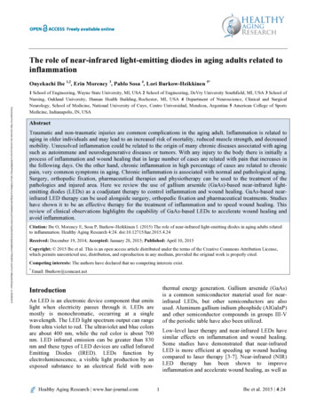
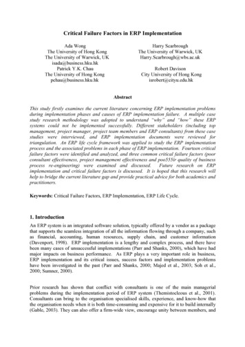
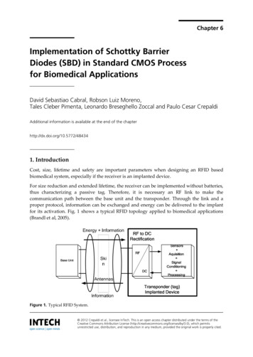
Chapter 6Implementation of Schottky BarrierDiodes (SBD) in Standard CMOS Processfor Biomedical ApplicationsDavid Sebastiao Cabral, Robson Luiz Moreno,Tales Cleber Pimenta, Leonardo Breseghello Zoccal and Paulo Cesar CrepaldiAdditional information is available at the end of the chapterhttp://dx.doi.org/10.5772/484341. IntroductionCost, size, lifetime and safety are important parameters when designing an RFID basedbiomedical system, especially if the receiver is an implanted device.For size reduction and extended lifetime, the receiver can be implemented without batteries,thus characterizing a passive tag. Therefore, it is necessary an RF link to make thecommunication path between the base unit and the transponder. Through the link and aproper protocol, information can be exchanged and energy can be delivered to the implantfor its activation. Fig. 1 shows a typical RFID topology applied to biomedical applications(Brandl et al, 2005).Figure 1. Typical RFID System. 2012 Crepaldi et al., licensee InTech. This is an open access chapter distributed under the terms of theCreative Commons Attribution License (http://creativecommons.org/licenses/by/3.0), which permitsunrestricted use, distribution, and reproduction in any medium, provided the original work is properly cited.
140 Biomedical Engineering – Technical Applications in MedicineAs it can be observed, the energy is transmitted by a pair of coupled coils. For patient safetyit is important to keep the induced electromagnetic fields at lower levels, to avoid tissuesdamages by raising the local temperature. The Specific Absorption Rate (SAR) representsdirect measurements of the electric field (indirect measurement of the magnetic field) andinduced current density over the human tissue at the implant location. The temperaturevariation over the time indicates the local heating factor. Both relations are given by (Pradieret al, 2005):SAR σE2ρdT SAR dtc W Kg (1) 0C s (2)where σ, ρ and c represent the conductivity, the human tissue mass density and specific heatcapacity, respectively, at the implant location. E is the incident electric field intensity (RMS).Based on equations (1) and (2), a safe value for the power transferred by the RF link is10mW/cm2.Besides cost and size reduction, microelectronics also allows the implementation of thetransponder circuits into a single die. The lowest prices can be achieved by using low coststandard CMOS technology.Transponder front-end circuits include a rectifier to make the AC-DC conversion to provideunregulated power supply to the tag. In CMOS technology, NMOS and PMOS (more oftenthan one of each type) transistors are used in different topologies to implement the rectifiercircuit. These devices, however, have the disadvantage of presenting a turn on thresholdvoltage (Vth) that may require larger induced voltage in the receiver coil. Although theCMOS technology has been minimizing the transistors geometries, the Vth voltage does notscale down at the same rate. The use of a Schottky Barrier Diode – SBD is an alternative wayto design the rectifier circuit in order to improve its efficiency. A more efficient rectifier willreduce the voltage drop between the tag input and the rest of the circuitry, thus reducingthe power demand from the transmitter. For low currents levels, typically found in this kindof application, the SBD voltage drop can be lower than a CMOS Vth voltage.The SBD is not readily implemented on a standard CMOS technology but after a fewadjustments in the masking process, it can be implemented. In this work, a mask sequence ispresented to implement SBDs in CMOS processes and a simple model for this device isdiscussed.2. Conventional rectifier circuitsBasically, RFID systems can be divided into three major groups: active, semi-passive andpassive tags. An active tag includes embedded batteries as their main energy source forautonomous operation. Semi-passive tags are also dependent on a battery for the start-up,
Implementation of Schottky Barrier Diodes (SBD) in Standard CMOS Process for Biomedical Applications 141however the required energy for the communication link is provided by the reader. Apassive tag, on the other hand, extracts the full power from the signal transmitted by thereader, thus there is no need of an on-board power supply. This autonomous capability ofpassive tags offers some interesting features such as low production cost, increasedreliability and a longer maintenance-free lifetime. The last one is very important consideringinherent surgical procedures related to an implanted device.A passive tag requires a circuit block to obtain the power transmitted from the base unit(known as reader) by the RF signal. This kind of circuit is a RF-DC converter or, simply,rectifier circuit.Mainly for passive tags, it is important to have a highly efficient RF to DC conversion (theRF energy received at the tag decreases rapidly as a function of distance from the reader)and it is also desired a stable power supply at the rectifier output.The available power at the tag antenna (PAVAIL) can be expressed by (Kotani and Takashi, 2009):2 λ PAVAIL PEIRPGTAG 4 d (3)where λ is the wavelength of the RF link, d is the distance between the base unit and the tag,PEIRP is the effective isotropic radiation power of the base unit transmitter, and GTAG is the tagantenna gain. The effective isotropic radiation power is determined by regulations, forinstance, 4W for electronic product code (EPC) protocol in North America.The tag antenna gain is manly determined by its area. Typically, GTAG is about 1.64 for a λ/2dipole type.In this scenario, the performance of the rectifier circuit, evaluated in terms of powerconversion efficiency (PCE) should be as large as possible. The PCE can be expressed as:PCErect PoutPin(4)where Pout is the output DC power circuit and Pin is the received RF input power.By combining eq. (3) and (4), and considering the presence of impedance matching, it ispossible to state the achievable power of an RFID tag: Ptag PEIRPGTAG PCErect 4 d 2(5)By analysing eq. (5) it is clear that the PCE is the most interesting variable to manipulate as away to obtain, for instance, an increase in the communication range d.In a typical RF-to-DC rectifier, PCE is mainly degraded as a result of two distinctmechanisms: forward voltage drop in the switches (closed related to the finite on-resistanceof this switches) and their leakage currents.
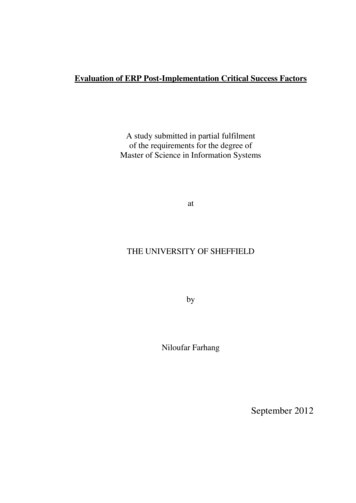
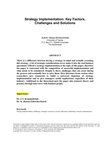
142 Biomedical Engineering – Technical Applications in MedicineAlthough typical RF-to-DC implementations also exhibit parasitic elements that contributeto lower the rectifier efficiency, they play a second-order effect.Rectifier circuits for RFID tags are usually Dickson based rectifiers and designed usingCMOS transistors. It must be clear that RFID applications are cost and area sensitive and thetag circuitry is often implemented in CMOS technologies that offer a high level ofintegration and relative low cost.The voltage drop of a diode-connected transistor is approximately the threshold voltage(Vth) of the MOS transistor. The literature presents few proposals to reduce the thresholdvoltage, known as “Vth cancelation”. One of then, the external-Vth-cancelation (EVC), wasproposed to for a semi-passive tag and depends on a gate bias voltage that is generated by aswitched-capacitor circuit. Since the operation is switched, it requires an external powersupply and clocking circuitry, and cannot be applied to passive-type RFIDs.The internal-Vth-cancelation (IVC) was also proposed. In this case, gate bias voltage isgenerated internally from the output DC voltage by a bias generation circuit. This circuitworks well under large input power conditions, but not otherwise since the gate biasvoltages are generated by a voltage division mechanism. Regarding the efficiency, the IVCcircuit dissipates an additional power due to the DC current, resulting in slightlydegradation in PCE.The self-Vth-cancelation (SVC) has the same topology of diode-connected CMOS rectifiercircuit except that gates of the nMOS transistor and PMOS transistor are connected to theoutput and ground terminal, respectively. This connection boosts the gate source voltage ofNMOS and PMOS transistors as much as possible, in other words, the threshold voltages aredecreased by the same amount as the output DC voltage. The SVC provides better PCE thanEVC and IVC implementations (Hashemi et al, 2012).Fig. 2 and 3 shows examples of a conventional CMOS diode-connected rectifier and self-Vthcancelation CMOS rectifier.RF inputCinRectified SignalM1M2Figure 2. Conventional CMOS Type Rectifier Circuit.Cout
Implementation of Schottky Barrier Diodes (SBD) in Standard CMOS Process for Biomedical Applications 143RF inputCinM1M2Rectified SignalCoutFigure 3. Self-Vth-Cancelation CMOS rectifier Circuit.Another rectifier is the “four-transistor-cell” CMOS rectifier, which outperforms CMOSdiode-based rectifiers, even when static Vth cancelation technique is used to reduce the turnon voltage of the diodes. In this configuration, the on-resistance of the CMOS transistors isdecreased by increasing gate-source voltage VGS and reverse leakage is reduced by reversingthe polarity of VDS in the cross-coupled structures. Fig. 4 illustrates an example of “fourtransistor-cell” rectifier.RF input Cin M1M2Rectified SignalCoutM3RF input -M4Cin-Figure 4. CMOS Four-Transistor-Cell Rectifier (Differential-Drive CMOS Rectifier).The drawback of the four-transistor-cell topology is that it does not perform well when thereceived RF power is in the range of few µW. This problem is more pronounced when thetag is implemented in low-cost CMOS technologies, where the threshold voltage of NMOSand PMOS transistors lays in range o few hundred mV. There is the possibility that thetransistors may not turn-on completely and the rectifier efficiency can be severely impaired.
144 Biomedical Engineering – Technical Applications in MedicineThe use of Schottky Barrier diodes in conventional Dickson rectifiers were considered as anattractive solution as a consequence of Schottky lower forward voltage drop and fastswitching speed . Although, this kind of device is not readily supported in almost all CMOStechnologies it is possible to be done with few mask flow changes. This chapter will showthat procedure on a low-cost CMOS technology.Fig. 5 shows the basic concept regarding a conventional Dickson rectifier with SBDs.Cn.Dn 1.C2Rectified SignalDnD4D3C1RF INputD2D1Cn 1Cn 2.Cn 3Figure 5. Basic Dickson Rectifier Circuit with SBD.3. Silicon based Schottky Barrier Diode (SBD)The Metal-Semiconductor contact (also called as Schottky Barrier Diode) has some featuresthat allow its use in high frequency applications and systems that must operate at lowvoltage levels. These features are, basically, the low level of minority charge accumulationduring commutation, which leads to high switching speeds and the low voltage dropbetween its terminals. Low turn on voltage, fast recovery time and low junction capacitanceare advantages that SBD offer over other types of PN diodes. These are the main reasonsthat SBD are so popular in RF applications. Fig. 6 shows the energy band diagram for thiskind of contact at thermal equilibrium. In this work, since we have used TSMC process, themetal is aluminium and the semiconductor is N-type, moderately doped, obtained by NWell diffusion (Janan et al, 2006), (Rainee and Philip, 2003) (Avenin, 1996).As can be seen, there is a build in contact potential Vbi expressed by:Vbi BN kT NC ln q N D (6)where kT/q is the thermal voltage (25.9mV at T 300K), NC is the effective state density(constant for a given temperature) in the conduction band, ND is the donor doping level andφBN is maximum height of the potential barrier (Streetman, 1980).
Implementation of Schottky Barrier Diodes (SBD) in Standard CMOS Process for Biomedical Applications 145q BN q M qVbiECWEFEVFigure 6. Energy Band Diagram for a Metal-Semiconductor Contact.Eq. (6) shows that the built in voltage Vbi can be reduced if a moderate to low dopingsemiconductor is used. Considering ideal values for metal work function (φM 4.28V) andsemiconductor electron affinity (χ 4V), the barrier φBN can be as low as 280mV. Considering,yet, eq. (6), the built in voltage Vbi can be further reduced by controlling the doping levelND.It must be necessary to evaluate the doping concentration ND in order to use eq. (6) to obtainVbi. For this procedure a C-V curve for a Metal-Insulator-Semiconductor (MIS capacitor))structure is used. Fig 7 and Fig. 8 show a typical MIS capacitor (with N type semiconductor)and a C-V curve, respectively.Figure 7. Metal-Insulator-Semiconductor (MIS) Capacitor.Figure 8. MIS C-V Curve.
146 Biomedical Engineering – Technical Applications in MedicineThe C-V curve can be obtained by simulating a PMOS transistor with TSMC modelparameters as indicated in Fig. 9.M1R1WLR2Figure 9. PMOS Transistor used to Plot C-V Curve.In this simulation, resistors R1 and R2 are very large in order to restrict the action of PMOSin the channel area. The DC source is swept from negative to positive voltage values, tovalidate all regions of operation of the MOS capacitor formed by the gate, insulator andchannel. The AC source can be set into low or high frequencies; therefore, it is possible toobtain the C-V curve behaviour as illustrated in Fig. 4.The capacitor area (A) is determined by the geometric aspect W and L of the PMOS transistor.The following equations are used to extract the doping concentration ND in a recursive way: C AWD max 1 0 S Cmin Cmax(7)4εS FND q 2WD(8) F kT N D ln q ni (9)where WD is the depth of depletion region formed in the contact, ε0 and εS are the vacuumand silicon dielectric permittivity, respectively, A the contact area (considering a parallelplate capacitor).The I-V characteristic of the Metal-Semiconductor structu
standard CMOS technology. Transponder front-end circuits include a rectifier to make the AC-DC conversion to provide unregulated power supply to the tag. In CMOS technology, NMOS and PMOS (more often than one of each type) transistors are used in different topologies to implement the rectifier circuit. These devices, however, have the disadvantage of presenting a turn on threshold