Transcription
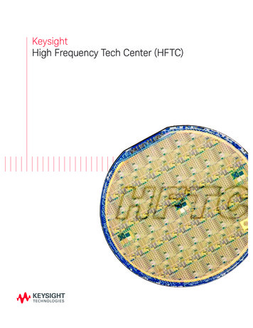
KeysightHigh Frequency Tech Center (HFTC)
IntroductionThe High Frequency Technology Center (HFTC) in Santa Rosa, California, invents, develops, accessesand manufactures world-leading custom integrated circuits. This gives Keysight a powerful competitive advantage and provides Keysight customers with premiere measurement solutions. HFTC has aunique combination of compound semiconductor fabrication capabilities (13,000 sq. ft. class-100 fab)and world-class expertise in design, modeling, measurement, and microfabrication. HFTC’s ability torapidly innovate and deliver the world’s best high frequency technology provides fundamental differentiation for electronic measurement products.
03 Keysight High Frequency Tech Center (HFTC)Core TechnologiesThe Tech Center offers a wide range of semiconductor technologies:– GaAsSb/InP DHBT (emitter CD of 1 µm, ƒT 200 GHz). General purpose digital/analog, signal conditioning chip-sets forinstrument frontends.– InGaP/GaAs HBT (emitter CD of 2 µm, ƒT 70 GHz). Generalpurpose digital/analog.– Solid State Switches (ultra fast settling). Up to 50 GHzswitches and attenuators.– GaAs junction and Schottky diode processes (based on InGaP/GaAs HBT platform).Signal conditioning, mixers, multipliers, switches.– GaAs/InGaAs/AlGaAs pHEMT (i-line and e-beam litho; gatelengths of 250 nm to 120 nm, ƒT 60 to 90 GHz). mm-waveLNAs, power ampliiers, switches.– GaAs FET (i-line litho; gate lengths of 350 nm, fT 30 GHz).Used for microwave power ampliiers and switches.– GaAs Thermocouple devices (wet etched web). Power sensorsfor power meters.– Next generation processes in development!Figure 1. 120 nm gate length PHEMT cross-sectionAll semiconductor technologies are available with passive circuitelements (high and low value thin ilm resistors, metal-insulator-metal capacitors), through-wafer vias, and multiple levels ofinterconnect.Technology AccessIn addition to internal materials growth and implant, HFTCroutinely accesses commercial vendors of novel semiconductormaterials many of which were co-developed between HFTC andstrategic suppliers.HFTC also accesses IC foundry services for technologies thatcan provide differentiation for Keysight instruments and complement internal capability. These technologies include GaN,very high performance pHEMTs, MEMS switches and advancedinterconnects.Figure 2. InP HBT IC with 3 levels of metal interconnects
04 Keysight High Frequency Tech Center (HFTC)Materials GrowthKeysight instruments offer outstanding performance that is often enabled by high speed/high frequency ICs built from III-Vsemiconductor materials – a core competency of the High Frequency Tech Center.Molecular Beam EpitaxyMaterial Characterization ToolsMolecular Beam Epitaxy (MBE) is a precise way of growingadvanced III-V semiconductors. Elements, from column III (Ga, Inand Al) and column V (As, Sb) of the periodic table, are combinedto produce: GaAs, AlAs, AlGaAs, InGaAs, InAlGaAs and GaAsSbsemiconductors. In these III-V semiconductors, carrier velocitiescan be large and energy bandgaps can be engineered to optimizecarrier transport and carrier coninement.Material growth is supported by a wide variety of characterizationtools, including:MBE growth takes place in an ultra-high vacuum (10 -10 Torr) environment that allows pure molecular beams to propagate withoutcollisions. Molecular beams are generated with heated elementalcells and focused onto heated GaAs or InP substrates.Epitaxial, or crystalline, growth takes place at elevatedsubstrate temperature of 450 600 C and at approximately2.8 Å/s. Individual shutters modulate the molecular beams andare capable of producing single atomic layers. Dopants (Si, Beor C) produce p-type or n-type semiconductor behavior. Ourcapabilities for MBE include:– One multi-wafer Veeco Gen200 (As)– One multi-wafer Veeco Gen200 (As, Sb) with in-situhydrogen plasma treatment capabilityFigure 3. Multi-wafer Gen 200 MBE system– Rigaku SmartLab x-ray diffraction, relection– Nanometrics RPM-blue production photoluminescence– Ultrahigh-sensitivity R&D photoluminescence andphotorelectance– Lehighton contactless conductivity mapping– 77 K and 300 K Hall measurements– Surface defect characterization– Phase-contrast optical microscopy
05 Keysight High Frequency Tech Center (HFTC)LithographyLithography capabilities include Nikonstepper-based projection lithography,contact lithography and E-beam lithography. In addition to the exposure tools,lithography processes include photoresistovens, coat/develop tracks and metrologytools. The combined toolset enables bothlift and etch mask processes on planarand non-planar surfaces with resist thicknesses ranging from 500 nm to 30 µmand critical dimensions (CDs) ranging from120 nm to 100 µm. Detailed capabilitiesare listed below.– Nikon NSR-2205i12D i-line (365 nm)stepper and TEL Mark Vz wafer tracksfor photoresist processing– 350 nm resolution– 65 nm x 3σ overlay– Lift-off and etch mask processes– JEOL JBX-6000FS E-beam system– Beam diameter 5 to 100 nm at50 KV– 60 nm x 2σ overlay– 120 nm gate lift-off for pHEMTs– Automated with up to 12 wafercassettes per load– EVG620 Automated Double Side MaskAlignment System and C&D P9000wafer track for photoresist coatingand developing– Backside via, backside scribe, andchip ID processes– Backside microscope alignments,IR thru wafer alignments and normal topside alignment capability– Up to 30 µm thick resist for backside via etch mask and selectiveplating mask. 1 µm CD in contactmodeFigure 4. 120 nm gate length PHEMT cross-sectionFigure 5. 700 nm JSR965/PMGI bilayer lithography
06 Keysight High Frequency Tech Center (HFTC)Dry EtchDry etch capability supports a wide varietyof tools and processes. Using photoresist, metal and dielectric masks, etchedCDs range from 120 nm to 60 µm, andetch depths range from 50 nm to 100µm. Etched materials include but are notlimited to: GaAs, InP, InGaP, InAlAs, GaAsSb, SiO2, Si3N4, BCB, W, and Ti/Pt/Au.Detailed capabilities are listed below.– Two SPTS high density plasma (HDP)etchers– Electrostatic chucks for precisetemperature control– High temperature etch capability– Laser endpoint for precise etchtermination with low exposed area– Three SPTS Omega general purposeRIE etchers– One SPTS Omega RIE etcher for deepGaAs etching such as backside viaswith a mechanically clamped chuck– Two Oxford PlasmaLab100 clustertools with multiple etch chambers,capable of high temperature operationand equipped with optical emissionand laser endpoint capabilities.– One IPE RIE etch tool with manualload capability to handle odd-sizedsubstrates– VEECO ion mill system that can produce 3 µm and 1.5 µm line and spaceon 2 µm and 1 µm thick Au-basedmetallization, respectively.Figure 6. HDP-etched 86 µm deep backside via in InPFigure 7. Oxford PlasmaLab 100 Etcher
07 Keysight High Frequency Tech Center (HFTC)DepositionDeposition processes support the application of thin ilms by sputter deposition,E-beam evaporation, ilament thermalevaporation, plasma enhanced chemicalvapor deposition (PECVD), spin-on coatingand electroplating. Material capabilitiesrange from highly conductive metals,through resistive thin ilms to insulating,planarizing and passivating dielectrics ofthicknesses ranging from 1 to 7 µm.– CVC and three TES sputter depositionsystems with in-situ ion-mill– Deposit Ti, Au, Ta2N, WSiNx, ,W,and TiW– CHA e-beam evaporator with in-situion mill deposits Ti, Pt, Au, Ni, Ge orAu/Ge– One Temescal BJD1800 e-beam evaporator for Ti, Pt, and Au deposition– Three Temescal long-throw e-beamevaporators, two with in-situ ionmill, for Ti, Pt, Au, Ni, Ge, and Modeposition– Three SPTS Delta PECVD systems– Load lock, cassette to cassetteoperation– SiNx and SiOx ilms from 50 to10,000 Å– Thickness uniformity 5%– Pre-deposition plasma surfaceconditioning– American Plating Systems Au platingbench– Cyanide-based Au platingsolution– Pulsed plating for conformalcoverage of backside vias– Selective backside plating– C&D P9000 Cluster System andSolitec 820 series tracks for interlayerdielectrics with hotplate and controlled atmosphere ovens for curing– HD Microsystems polyimide 1 to2 µm thick– Dow Cyclotene (BCB) 2 to 7 µmthickFigure 8. CVC sputter deposition systemFigure 9. Temescal FCE-2800
08 Keysight High Frequency Tech Center (HFTC)Wet Etch and LiftWet etch and lift processes support precise material removal byeither etching semiconductors, metals and dielectrics or dissolving organic lift structures.– Four Universal Plastics wet etch stations– Robotic tank-to-tank cassette transfer– Temperature, recirculation and agitation control– Quick dump and spray rinsing capability– Two Electroglas wafer-probe stations for gate recess currenttargeting– SSEC WaferEtch system for cassette-to-cassette spray etchcapability– SPEC automatic solvent lift-off tool– Computer controlled cassette-to-cassette– Temperature control, recirculation/iltration, agitationcontrol, ultrasonic transducers– Five process tanks and spin dryer– MCE Leonardo 200LO Tape Lift Tool for cassette-to-cassettedry lift-off process– Eco–Snow WaferClean 1600 for metal lift-off and surfaceclean-up– Microprocess Technologies and Semitool Spray Solvent ToolsFigure 11. MCE 200LO Tape Lift ToolWafer ThinningBefore backside processing, wafers are thinned by lapping andpolishing GaAs or InP to either 50 or 100 µm.– Two Engis FL15 Lappers– Lapmaster and Strasbaugh polishers– Digimatic micrometer and precision laser gauge for thicknesscontrolFigure 10. Automated lift toolFigure 12. Engis FL15 lapper
09 Keysight High Frequency Tech Center (HFTC)Characterization ToolsThe wafer and die fabs depend on a broad range of characterization tools for process monitoring and diagnostics. Metrology toolsincluding analytical SEMs, metrology SEMs, and IVS-120 monitorcritical CDs down to 100 nm. Other tools include AFM, optical ilmthickness metrology, proilometers, contactless conductivity meters, contact angle test system, surface particle monitors, Augeranalysis, and energy-dispersive x-ray analysis (EDX).– Auriga Crossbeam and LEO 1550 Analytical SEMs– High resolution SEM images to 5 nm– EDX for elemental characterization– FIB and STEM capability for extremely high resolutioncross-sections. Automated multiple cross-section moviecreation.– Hitachi S6100 and S6200H low voltage linewidth metrologySEMs– Semi-automatic operation and linewidth analysis for CDmeasurements from tens of µm to below 100 nm– Cassette-to-cassette operation for 75 and 100 mmwafers; manual operation for smaller samples– Agilent Technologies 5600LS Scanning Probe Microscope– Provides detailed surface height and lateral dimensions ofsamples down to the Ångstrom level– Capabilities include: Atomic Force Microscopy (AFM),Scanning Tunneling Microscopy, Current Sensing AFM,Lateral Force Microscopy, Electrostatic Force Microscopy,Kelvin Force Microscopy, High Temperature Chuck– Rudolph S-200 and SCI FilmTek 2000 spectroscopic opticalilm thickness metrology tools– Thickness of transparent ilms from Ångstroms to tens ofµm, and semiconductor ilms to hundreds of Ångstroms– Relectometry and multi-wavelength ellipsometry– Automatic cassette-to-cassette operation with patternrecognition for in-process measurements– IVS-120 optical linewidth and overlay metrology tool– Overlay measurements for the control of stepperlithography to nm levels– Optical linewidth measurements to the µm level– Automatic cassette-to-cassette operation with patternrecognition– other tools– Phi 660 Auger Electron Spectroscopy System providing surface elemental composition mapping and depthproiling– Four-point probe for metal sheet resistance– Contactless conductivity for semiconductor and metalsheet resistance– Tencor proilometer for ilm thickness and etched stepheight characterization from 10s of nm - 100s of µm.– Contact-angle metrology tool for measuring materialsurface energy, cleanliness and wettingFigure 13. Zeiss Auriga FIB SystemIsolation region around HB2A emitter metalCurrent sensing AFMTapping mode AFMFigure 14. AFM image of 2x2 µm2 HBT showing implant isolation region
10 Keysight High Frequency Tech Center (HFTC)Die FabAfter wafer processing through thinningand backside steps, wafers are transferred to the Die Fab where, after on-wafertest, individual chips are separated (singulation) by sawing for production masksand laser cutting for prototype masks.Capabilities also include inking of rejecteddie, die sorting, and visual inspection.– August Technology NSX-90 autovisualsystem– Intelligent screening of 500 nm orlarger defects– 10,000 die/hr inspection throughput– K&S 982 diamond saws with 60 µm kerf– 3D Micromac laser micro-machiningsystem with Lumera Hyper Rapid25 picosecond source– Quantronix Model 116 Nd:YAG lasersystem– Arbitrary orthogonal streets with40 µm kerf for semiconductors– Arbitrary laser shaping of alumina,sapphire, and other materials– Laurier 3000 and DS4000 autosortsystems– Royce Instruments DE35 manual sortsystems– Ultrasonic drilling (254 µm) in glassand ceramicsFigure 15. 3DMicromac Laser System for wafer separationSurface Mount PackagingHFTC provides most of its ICs in economical surface mount packaging compatiblewith industry-standard printed circuitboard assembly. SMT package attributesinclude:– Small, leadless, plastic moldedcomponents with up to 40 I/Os and 26 GHz performance at differentiatingprice points– Concurrent IC/package design is exercised to shorten the time to market .– RoHS compliant & compatible– Electrical testing in house usingKeysight measurement equipment toensure quality– Extensive environmental qualiicationsand sample auditing to deliver consistent reliability– S-Parameter data, reference designs,and evaluation boards availableFigure 16. Laser separated IC chipsFigure 17. QFN package
11 Keysight High Frequency Tech Center (HFTC)Electrical Test & MeasurementHFTC ensures total quality by electrically testing each semiconductor product we ship to our customers. Our testing expertiseand capabilities are extensive: customized hardware and softwareand proprietary measurement algorithms augment a suite of Keysight test and measurement equipment. Electrical testing occursat three stages in our manufacturing process: in-process wafertest, product test, and reliability monitoring.Wafer TestHFTC monitors the quality of each wafer by testing process control monitors (PCMs) at multiple steps in the fabrication process.Data from these tests enable robust statistical process control(SPC) for each unit process and facilitate our wafer acceptanceprogram. Wafers meeting stringent acceptance criteria areapproved for further processing. Rejected wafers are analyzedfor failure modes. Four PCM test platforms reside inside ourclass-100 clean room facility. Capabilities include:Figure 18. Automated on-wafer MMIC test station– Parametric dc I-V and C-V characterization– High resolution– 150 C maximum ambient temperature– Multi-wafer cassette-loading autoprobers– RF network and spectral analysis to 50 GHz– Automatic model parameter extraction– Coincident physical and mathematical reference planesProduct TestFull electrical qualiication (100% known good die) of inishedparts to data sheet speciications ensures the integrity of Keysight’s internal semiconductor supply chain. There are sevenmajor test platforms comprising 18 ESD-safe test stations. Capabilities and features include:– Flexible on-wafer probing conigurations– Single and multi-wafer cassette-loading autoprobers– Capabilities for quad probes and probe cards– Flexible dc bias conigurations – up to 48 connectionsstandard– Variable RF input and output (I/O) conigurations - upto four single or dual RF probes with multiple signal andground conigurations standard– 100 µm minimum dc and RF pad spacing– On-wafer parametric dc I-V and C-V characterization– On-wafer frequency-domain characterization of analog andmicrowave components– Network analysis to 110 GHz– Vector-corrected frequency-conserving spectral analysisto 50 GHz– Scalar-corrected frequency-translating multi-tonespectral analysis to 75 GHz– Low-frequency noise characterization to 100 MHzFigure 19. RF and dc on-wafer probes– On-wafer time-domain characterization of digital andmixed-signal components– Pulse or pattern stimuli to 32 Gb/s– Level or pattern trigger– Waveform capture and analysis– Packaged product and multi-chip module (MCM)qualiication– Automated package handler– Multiple plastic and ceramic package and MCM types,including industry standard QFN– Lead-spring, package-test ixture interfaces standard– Wirebond continuity testing to 20 GHz– Tape and reel and tray shipping formats
12 Keysight High Frequency Tech Center (HFTC)Reliability MonitoringTest Management SystemConsistent with our ongoing commitment to industry-leadinginstrument grade quality, HFTC monitors the long-term reliabilityof semiconductor processes by accelerated life testing individualdie from production wafers. Our capabilities include:The test management system is a lexible .NET Windows- basedtest software platform. It can easily be extended and customizedto meet speciic requirements for wafer test, product test, packaged product test, and reliability test. Key features:– High-Temperature Operating Life (HTOL)– Stresses die at elevated temperature – up to 260 C– Electromigration of chassis interconnects– Data used to estimate IC lifetime for instrumenttype-o: grade applications.– Medium Scale Integration (MSI) Array– Identiies transistor and/or interconnect infant failures– Over 12,000 transistors are typically tested per wafer– RF operating life (RFOL)– Mimics actual use-case environment (power andfrequency)– Records evolution of output power drift vs. time– High Voltage Array (HVA)– Screens out wafers with potential high voltage operationissues– 1,600 transistors typically tested per wafer– Time Dependent Dielectric Breakdown (TDDB) for capacitors– Lifetime correlated to voltage ramp-rate and breakdown– Test conducted in wafer fab for expedient feedback– Engineers can quickly develop electrical tests seamlesslyin runtime and design-time environments– Advanced debugging supports easy discovery andvalidation of code– Promotion of reuse of proprietary drivers and measurement algorithms across test process centers– Test code can be conigured to test a multitude of protoand production products, minimizing code maintenanceand support– Built-in version control system and tagged version distribution serviceFigure 20. Reliability lab
13 Keysight High Frequency Tech Center (HFTC)Technical Data ManagementModeling and Measurement SciencesA comprehensive manufacturing execution system, of which ourelectrical test platforms are a part, supports the HFTC manufacturing and engineering operations. Our data infrastructure storesunit process lows, wafer routings, operator comments, waferacceptance logs, and PCM and product test data. In addition, adata mining, manipulation, and delivery system places appropriately distilled statistical process and product data in the hands ofengineers and managers. Combined, these systems manage all ofour technical data. Features:Successful design low of world class ICs depends on the abilityto measure, characterize and extract models for our devices(from a single junction to a complex MMIC). Accurate measurements and models allow new designs to converge towards thedesired performance level in a minimum number of iterations(typically 1-3), accelerating time to market and reducing costlywafer turns.– Integrated manufacturing executive system (MES)– Guides manufacturing process from beginning to end –from wafer start to product shipment– Supports unique requirements of lot-based multistepwafer processing on a common toolset– Flexible data infrastructure– Common database family for all products– Hierarchically deined data – raw or summary data andspeciication limits for multiple DUT families, each withmultiple DUT types, at multiple process steps– Complete suite of statistical analysis tools– Automated statistical reports – wafer acceptance,parameter yield, boxplot trend, and others– Powerful statistical process control (SPC) analysis tools– Generic statistical engine with customized GUI andplotting scripts– Seamless correlation between multiple data sets –PCM data versus product dataThe creation of exceptionally accurate models for tomorrow’sdevices requires measurements that often push the limits of testequipment available today. HFTC measurement facilities includea leading-edge engineering test lab which houses an extensivearray of general purpose and custom test stations speciicallydesigned to enhance the R&D development test experience,reducing setup times, and accelerating test throughput for MMICdesigners, package and module developers, and product supportengineers alike. The wide-array of test capabilities incorporatedinto this highly-eficient test lab includes:Finally, an experienced team of hardware and software engineering team manage our test and data capabilities. HFTC strives toproperly balance performance, lexibility and cost for an optimized customer solution.Measurements– Vector-corrected frequency-conserving spectral analysis to110 GHz– On-wafer scalar spectral analysis to 170 GHz– Time domain characterization at any data rate through52 Gb/s– Sub-µsec, pulsed S-parameter measurements through50 GHz– Linear and non-linear vector network analysis for DynaFET,X-Parameter, FET, and HBT Model extractions– High power ACPR, TOI, and power strife custom HW set ups– Multiple, multi-port on-wafer probe stations with customcalibration through 50, 67 and 110 GHz.– Coaxial and on-wafer LFO and Phase Noise characterizationcapabilities– Non-linear, active and passive load pull capabilities to50 GHz– Device and package ESD and overvoltage stresscharacterization– Microwave and mmWave RFOL stress stations– MMIC and device auto probers with wide-range temperaturecontrolMeasurements across a variety of parameters (bias, frequency,power, sizes and temperatures) are inally required to provide amodel capable of reproducing nominal performance variationsonce in production.Figure 21. Engineering Test Lab
14 Keysight High Frequency Tech Center (HFTC)ModelingModel deinition is the interpretation of solid measured data, hypothesizing theunderlining mechanisms via:– Equivalent circuits (compact model)– Behavioral (neural networks)– S-parameters & X-parametersModels are reined to match device performance across a broad range of conditions andare incorporated in Keysight’s EDA CAD tools.Measurement and modeling science is at the core of accurate CAD tools, providingunmatched accuracy under large and small signals, pulsed conditions, and non-50-Ohmapplications.While providing internal beneit to Keysight, HFTC-driven modeling activities have alsoestablished industry standards. In 2009, HFTC developed X-parameters, a mathematicalsuperset of S-parameters. Like S-parameters, X-parameters enable the measurementand modeling of microwave components in a scalable and cascadable manner. UnlikeS-parameters, X-parameters include non-linear, multi tone, and not-Z0 impedance loadconditions. This enables modeling and measurements of device characteristics thatwere previously dificult or impractical.Externally available ICsIn addition to providing Keysight with world leading ICs, HFTC also sells a broad range ofICs externally, both bare die and packaged. The product offering features componentswith broadband frequency coverage and high linearity including:– Highly linear mixers– High power/high idelity ampliiers– High TOI attenuators
15 Keysight High Frequency Tech Center (HFTC)myKeysightwww.keysight.com/find/mykeysightA personalized view into the information most relevant to you.www.keysight.com/go/qualityKeysight Technologies, Inc.DEKRA Certified ISO 9001:2008Quality Management SystemHFTC is at the cutting edge of technology, providing criticalhigh frequency solutions for the world’s premiere electronicsmeasurement company.For more information, please visit:www.keysight.com/ind/mmicFor more information on KeysightTechnologies’ products, applications orservices, please contact your local Keysightoffice. The complete list is available azilMexicoUnited States(877) 894 441455 11 3351 7010001 800 254 2440(800) 829 4444Asia PaciicAustraliaChinaHong KongIndiaJapanKoreaMalaysiaSingaporeTaiwanOther AP Countries1 800 629 485800 810 0189800 938 6931 800 112 9290120 (421) 345080 769 08001 800 888 8481 800 375 81000800 047 866(65) 6375 8100Europe & Middle rlandUnited Kingdom0800 0011220800 585800800 5232520805 9803330800 62709991800 8327001 809 343051800 599100 32 800 585800800 02332008800 5009286800 0001540200 8822550800 805353Opt. 1 (DE)Opt. 2 (FR)Opt. 3 (IT)0800 0260637For other unlisted -14)This information is subject to change without notice. Keysight Technologies, 2015Published in USA, April 8, 20155992-0385EN (Rev 1.5)www.keysight.com
The High Frequency Technology Center (HFTC) in Santa Rosa, California, invents, develops, accesses and manufactures world-leading custom integrated circuits. This gives Keysight a powerful compet- . - Phase-contrast optical microscopy Materials Growth Molecular Beam Epitaxy Molecular Beam Epitaxy (MBE) is a precise way of growing
