Transcription
C 8 0 5 1 F5 2 x - 5 3 x - DKC8051F52 X -53 X D EVELOPMENT K IT U S E R ’ S G U I D E1. Relevant DevicesThe C8051F52x-53x Development Kit is intended as a development platform for the microcontrollers in theC8051F52x-53x MCU family. The members of this MCU family are C8051F520, C8051F521, C8051F523,C8051F524, C8051F526, C8051F527, C8051F530, C8051F531, C8051F533, C8051F534, C8051F536 andC8051F537.Notes: The target board included in this kit is provided with two pre-soldered C8051F530-IT MCUs (TSSOP-20package). Code developed on the C8051F530 can be easily ported to the other members of this MCU family. Refer to the C8051F52x-53x data sheet for the differences between the members of this MCU family.2. Kit ContentsThe C8051F52x-53x Development Kit contains the following items: C8051F530 Target Board C8051Fxxx Development Kit Quick-Start Guide Silicon Laboratories IDE and Product Information CD-ROM. CD content includes: Silicon Laboratories Integrated Development Environment (IDE) Keil 8051 Development Tools (macro assembler, linker, evaluation ‘C’ compiler) Source code examples and register definition files Documentation C8051F52x-53x Development Kit User’s Guide (this document) AC to DC Power Adapter USB Debug Adapter (USB to Debug Interface) USB CableThe development kit target board contains two C8051530 microcontrollers that can communicate through a LINnetwork. One of the C8051F530 (U1) can also be connected to a CP2102 USB to UART bridge while the other one(U2) can be directly connected to two analog signals and a Voltage Reference Signal Input.The kit is provided with one USB Debug Adapter but the designer can add a second USB debug adapter so thatboth microcontrollers can have their firmware debugged at the same time using only one PC and two instances ofthe Silicon Labs IDE.Rev. 0.2 12/07Copyright 2007 by Silicon LaboratoriesC8051F52x-53x-DK
C8051F52x-53x-DK3. Getting StartedAll software required to develop firmware and communicate with the target microcontroller is included in the CDROM. The CD-ROM also includes other useful software.Below is the software necessary for firmware development and communication with the target microcontroller: Silicon Laboratories Integrated Development Environment (IDE)Keil 8051 Development Tools (macro assembler, linker, evaluation C compiler)Other useful software that is provided in the CD-ROM includes the following:Configuration Wizard 2Keil uVision Drivers CP210x USB to UART Virtual COM Port (VCP) Drivers 3.1. Software InstallationThe included CD-ROM contains the Silicon Laboratories Integrated Development Environment (IDE), Keil software8051 tools and additional documentation. Insert the CD-ROM into your PC’s CD-ROM drive. An installer willautomatically launch, allowing you to install the IDE software or read documentation by clicking buttons on theInstallation Panel. If the installer does not automatically start when you insert the CD-ROM, run autorun.exe foundin the root directory of the CD-ROM. Refer to the ReleaseNotes.txt file on the CD-ROM for the latest informationregarding known problems and restrictions. After installing the software, see the following sections for informationregarding the software and running one of the demo applications.3.2. CP210x USB to UART VCP Driver InstallationThe C8051F530 target board includes a Silicon Laboratories CP2102 USB-to-UART Bridge Controller. Devicedrivers for the CP2102 need to be installed before PC software such as HyperTerminal can communicate with thetarget board over the USB connection. If the "Install CP210x Drivers" option was selected during installation, thiswill launch a driver “unpacker” utility.1. Follow the steps to copy the driver files to the desired location. The default directory is C:\SiLabs\MCU\CP210x.2. The final window will give an option to install the driver on the target system. Select the “Launch the CP210xVCP Driver Installer” option if you are ready to install the driver.3. If selected, the driver installer will now launch, providing an option to specify the driver installation location. Afterpressing the “Install” button, the installer will search your system for copies of previously installed CP210xVirtual COM Port drivers. It will let you know when your system is up to date. The driver files included in thisinstallation have been certified by Microsoft.4. If the “Launch the CP210x VCP Driver Installer” option was not selected in step 3, the installer can be found inthe location specified in step 2, by default C:\SiLabs\MCU\CP210x\Windows 2K XP S2K3 Vista. At thislocation, run CP210xVCPInstaller.exe.5. To complete the installation process, connect the included USB cable between the host computer and the USBconnector (P1) on the C8051F530 target board. Windows will automatically finish the driver installation.Information windows will pop up from the taskbar to show the installation progress.6. If needed, the driver files can be uninstalled by selecting “Silicon Laboratories CP210x USB to UART Bridge(Driver Removal)” option in the “Add or Remove Programs” window.2Rev. 0.2
C8051F52x-53x-DK4. Software Overview4.1. Silicon Laboratories IDEThe Silicon Laboratories IDE integrates a source-code editor, a source-level debugger, and an in-system Flashprogrammer. See Section 6., "Using the Keil Software 8051 Tools with the Silicon Laboratories IDE‚" on page 6 fordetailed information on how to use the IDE. The Keil Evaluation Toolset includes a compiler, linker, and assemblerand easily integrates into the IDE. The use of third-party compilers and assemblers is also supported.4.1.1. IDE System RequirementsThe Silicon Laboratories IDE requirements: Pentium-class host PC running Microsoft Windows 2000 or newer. One available USB port. 64 MB RAM and 40 MB free HD space recommended.4.1.2. Third Party ToolsetsThe Silicon Laboratories IDE has native support for many 8051 compilers. The full list of natively supported tools isas follows: Keil IAR Raisonance Tasking Hi-Tech SDCCThe demo applications for the C8051F530 target board are written to work with the Keil and SDCC toolsets.4.2. Keil Evaluation Toolset4.2.1. Keil Assembler and LinkerThe assembler and linker that are part of the Keil Demonstration Toolset are the same versions that are found inthe full Keil Toolset. The complete assembler and linker reference manual can be found on-line under the Helpmenu in the IDE or in the “SiLabs\MCU\hlp” directory (A51.chm).4.2.2. Keil Evaluation C51 C CompilerThe evaluation version of the C51 compiler is the same as the full version with the following limitation: (1) Maximum4 kB code generation. When installed from the CD-ROM, the C51 compiler is initially limited to a code size of 2 kB,and programs start at code address 0x0800. Refer to the Application Note “AN104: Integrating Keil Tools into theSilicon Labs IDE" for instructions to change the limitation to 4 kB, and have the programs start at code address0x0000.Rev. 0.23
C8051F52x-53x-DK4.3. Configuration Wizard 2The Configuration Wizard 2 is a code generation tool for all of the Silicon Laboratories devices. Code is generatedthrough the use of dialog boxes for each of the device's peripherals.Figure 1. Configuration Wizard 2 UtilityThe Configuration Wizard 2 utility helps accelerate development by automatically generating initialization sourcecode to configure and enable the on-chip resources needed by most design projects. In just a few steps, the wizardcreates complete startup code for a specific Silicon Laboratories MCU. The program is configurable to provide theoutput in C or assembly. For more information, refer to the Configuration Wizard 2 help available under the Helpmenu in Config Wizard 2.4.4. Keil uVision2 and uVision3 Silicon Laboratories DriversAs an alternative to the Silicon Laboratories IDE, the uVision debug driver allows the Keil uVision IDE tocommunicate with Silicon Laboratories on-chip debug logic. In-system Flash memory programming integrated intothe driver allows for rapidly updating target code. The uVision IDE can be used to start and stop programexecution, set breakpoints, check variables, inspect and modify memory contents, and single-step throughprograms running on the actual target hardware.4Rev. 0.2
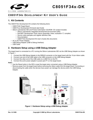
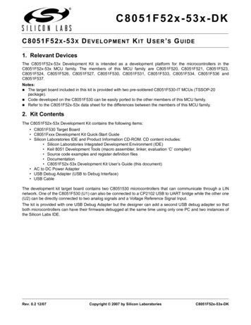
C8051F52x-53x-DK5. Hardware Setup Using a USB Debug AdapterThe target board is connected to a PC running the Silicon Laboratories IDE via the USB Debug Adapter as shownin Figure 2.1. Connect the USB Debug Adapter to one of the DEBUG connectors on the target board (HDR1 or HDR2)with the 10-pin ribbon cable. The recommended connection is to the HDR1 (connected to U1) as this microcontroller can be connected to the CP2102 USB to UART bridge.2. Connect one end of the USB cable to the USB connector on the USB Debug Adapter.3. Connect the other end of the USB cable to a USB Port on the PC.4. Connect the ac/dc power adapter to power jack P5 on the target board.Notes: Use the Reset button in the IDE to reset the target when connected using a USB Debug Adapter. Remove power from the target board and the USB Debug Adapter before connecting or disconnecting theribbon cable from the target board. Connecting or disconnecting the cable when the devices have power candamage the device and/or the USB Debug J2HDR42“B” SIDE1RDH2“A” SIDE11P1.4 AJ1P1.4 BC8051T530 TBU2SILICON LABORATORIESF530JTAGHDR3J5D1RESET ARunStopSilicon LaboratoriesUSB DEBUG ADAPTERPowerUSBCableHDR2Target BoardRESET BP5USB Debug AdapterJ3PCPrototypeAreaFigure 2. Hardware Setup using a USB Debug AdapterRev. 0.25
C8051F52x-53x-DK6. Using the Keil Software 8051 Tools with the Silicon Laboratories IDETo perform source-level debugging with the IDE, you must configure the Keil 8051 tools to generate an absoluteobject file in the OMF-51 format with object extensions and debug records enabled. You may build the OMF-51absolute object file by calling the Keil 8051 tools at the command line (e.g. batch file or make file) or by using theproject manager built into the IDE. The default configuration when using the Silicon Laboratories IDE projectmanager enables object extension and debug record generation. Refer to Application Note "AN104: Integrating Keil8051 Tools into the Silicon Labs IDE" in the “SiLabs\MCU\Documentation\ApplicationNotes” directory for additionalinformation on using the Keil 8051 tools with the Silicon Laboratories IDE.To build an absolute object file using the Silicon Laboratories IDE project manager, you must first create a project.A project consists of a set of files, IDE configuration, debug views, and a target build configuration (list of files andtool configurations used as input to the assembler, compiler, and linker when building an output object file).The following sections illustrate the steps necessary to manually create a project with one or more source files,build a program and download the program to the target in preparation for debugging. (The IDE will automaticallycreate a single-file project using the currently open and active source file if you select Build/Make Project before aproject is defined.)6.1. Creating a New Project1. Select Project New Project to open a new project and reset all configuration settings to default.2. Select File New File to open an editor window. Create your source file(s) and save the file(s) with arecognized extension, such as .c, .h, or .asm, to enable color syntax highlighting.3. Right-click on “New Project” in the Project Window. Select Add files to project. Select files in the file browserand click Open. Continue adding files until all project files have been added.4. For each of the files in the Project Window that you want assembled, compiled, and linked into the target build,right-click on the file name and select Add file to build. Each file will be assembled or compiled as appropriate(based on file extension) and linked into the build of the absolute object file.Note: If a project contains a large number of files, the “Group” feature of the IDE can be used to organize. Right-click on “NewProject” in the Project Window. Select Add Groups to project. Add pre-defined groups or add customized groups.Right-click on the group name and choose Add file to group. Select files to be added. Continue adding files until allproject files have been added.6.2. Building and Downloading the Program for Debugging1. Once all source files have been added to the target build, build the project by clicking on the Build/MakeProject button in the toolbar or selecting Project Build/Make Project from the menu.Note: After the project has been built the first time, the Build/Make Project command will only build the filesthat have been changed since the previous build. To rebuild all files and project dependencies, click on theRebuild All button in the toolbar or select Project Rebuild All from the menu.2. Before connecting to the target device, several connection options may need to be set. Open the ConnectionOptions window by selecting Options Connection Options . . . in the IDE menu. First, select theappropriate adapter in the “Serial Adapter” section. Next, the correct “Debug Interface” must be selected.C8051F52x-53x family devices use the Silicon Labs 2-wire (C2) debug interface. Once all the selections aremade, click the OK button to close the window.3. Click the Connect button in the toolbar or select Debug Connect from the menu to connect to the device.4. Download the project to the target by clicking the Download Code button in the toolbar.Note: To enable automatic downloading if the program build is successful, select Enable automatic connect/download after build in the Project Target Build Configuration dialog. If errors occur during the buildprocess, the IDE will not attempt the download.5. Save the project when finished with the debug session to preserve the current target build configuration, editorsettings, and the location of all open debug views. To save the project, select Project Save Project As . . .from the menu. Create a new name for the project and click on Save.6Rev. 0.2
C8051F52x-53x-DK7. Example Source CodeExample source code and register definition files are provided in the “SiLabs\MCU\Examples\C8051F52x 53x”directory during IDE installation. These files may be used as a template for code development. Exampleapplications include a blinking LED example which configures the green LED on the target board to blink at a fixedrate.7.1. Register Definition FilesRegister definition files, C8051F530.inc and C8051F530.h, define all SFR registers and bit-addressable control/status bits. They are installed into the “SiLabs\MCU\Examples\C8051F52x 53x” directory during IDE installation.The register and bit names are identical to those used in the C8051F52x-53x data sheet. Both register definitionfiles are also installed in the default search path used by the Keil Software 8051 tools. Therefore, when using theKeil 8051 tools included with the development kit (A51, C51), it is not necessary to copy a register definition file toeach project’s file directory.7.2. Blinking LED ExampleThe example source files, blink.asm and blinky.c, show examples of several basic C8051F52x-53x functions.These include: disabling the watchdog timer (WDT), configuring the Port I/O crossbar, configuring a timer for aninterrupt routine, initializing the system clock, and configuring a GPIO port. When compiled/assembled and linked,this program flashes the green LED on the C8051F530 target board associated with the microcontroller about fivetimes a second using the interrupt handler with a C8051F530 timer.Rev. 0.27
C8051F52x-53x-DK8. Target BoardThe C8051F52x-53x Development Kit includes a target board with two C8051F530 devices pre-installed forevaluation and preliminary software development. Numerous input/output (I/O) connections are provided tofacilitate prototyping using the target board. Refer to Figure 3 for the locations of the various I/O connectors.Power connector (Accepts input from 7 to 15 VDC unregulated power adapter.)RED Power-on LEDLIN connectorJ1HDR1P1D1Reset AP1.4 AHDR3J7T1U224-pin Expansion I/O connector for U2 (side A)Debug connector for Debug Adapter Interface (side A - U2)USB connector to serial interface (CP2102)Green LED (side A, U2), P1.3-AReset button (side A, U2)Push button (side A, U2)Connector block for serial port connection, Green LED, and push-button Side APower connection block selection for the CP2102LIN transceiver (side A - U2)C8051F530 side AJ2HDR2P1.4-BJ5T2Reset BU1TB2HDR4D2J3J424-pin Expansion I/O connector for U1 (side B)Debug connector for Debug Adapter Interface (side B - U1)Push button (Side B, U1)VREFIN connector blockLIN transceiver (side B - U1)Reset button (side B, U1)C8051F530 side BAnalog input connectorGreen LED and push-button connector block, Side BGreen LED (side B, U1), P1.3 BChannel 1, P1.6 B connector blockChannel 2, P1.7 B connector blockRESET B“B” SIDEF530T2U1SILICON LABORATORIEST1D3HDR4P1.4 51T530 TB“A” SIDEF530P5D1HDR3J7U21P1RESET AHDR1JTAGJ12P1.4 AFigure 3. C8051F530 Target Board8Rev. 0.2
C8051F52x-53x-DK8.1. System Clock SourcesThe C8051F530 device installed on the target board features a calibrated programmable internal oscillator which isenabled as the system clock source on reset. After reset, the internal oscillator operates at a frequency of3.0625 MHz ( 0.5%) by default but may be configured by software to operate at other frequencies. Therefore, inmany applications an external oscillator is not required. However, if you wish to operate the C8051F530 device at afrequency not available with the internal oscillator, an external crystal may be used. Refer to the C8051F52x-53xdata sheet for more information on configuring the system clock source.The target board is designed to facilitate the installation of external crystals. Install the crystals at the pads markedY1 or Y2. Install a 10 MΩ resistor at R17 or R22 and install capacitors at (C29 and C30) or (C34 and C35) usingvalues appropriate for the crystals you select. Refer to the C8051F52x-53x data sheet for more information on theuse of external oscillators.8.2. Switches and LEDsFour switches are provided on the target board.Switch RESET A is connected to the RESET pin of the C8051F530 A-Side (U2).Switch RESET B is connected to the RESET pin of the C8051F530 B-Side (U1).Pressing RESET A or RESET B puts the attached device into its hardware-reset state.Switches P1.4 A and P1.4 B are connected to the C8051F530 parts (U1 and U2) general purpose I/O (GPIO) pinsthrough headers. Pressing P1.4 A or P1.4 B generates a logic low signal on the port pin of the respectivemicrocontroller.Remove the shorting block from the header to disconnect P1.4 A or P1.4 B from the port pins. The port pinsignals are also routed to pins on the J1 and J2 I/O connectors. See Table 1 for the port pins and headerscorresponding to each switch.Three LEDs are also provided on the target board. The red LED labeled WR is used to indicate a power connectionto the target board. The green LEDs labeled D1 and D2 are connected to the C8051F530's GPIO pins throughheaders. Remove the shorting blocks from the headers to disconnect the LEDs from the port pins. The port pinsignals are also routed to pins on the J1 and J2 I/O connectors. See Table 1 for the port pins and headerscorresponding to each LED.Table 1. Target Board I/O DescriptionsDescriptionI/OHeaderReset AReset BP1.4 AP1.4 BGreen LED D1Green LED D2Red 2]noneRev. 0.29
C8051F52x-53x-DK8.3. Expansion I/O Connectors (J1, J2)The two 24-pin Expansion I/O connectors J1 and J2 provide access to all signal pins of the C8051F530 devices.Pins for VDD, GND, 5 V, Reset, Vbat, LIN, 3.3 V and Vrefin are also available. A small through-hole prototypingarea is also provided.All I/O signals routed to connectors J1 and J2 are also routed to through-hole connection points between J1 and J2and the prototyping area (see Figure 3 on page 8). Each connection point is labeled indicating the signal availableat the connection point. See Table 2 for a list of pin descriptions for J1 and J2.Table 2. Pin Descriptions for J1 and J2J1J2Pin #DescriptionPin #DescriptionPin #DescriptionPin #Description1P0.0 A13P1.4 A1P0.0 B13P1.4 B2P0.1 A14P1.5 A2P0.1 B14P1.5 B3P0.2 A15P1.6 A3P0.2 B15P1.6 B4P0.3 A16P1.7 A4P0.3 B16P1.7 B5P0.4 A17 5V5P0.4 B17 5V6P0.5 A18RST/C2CLK A6P0.5 B18RST/C2CLK B7P0.6 A19VBAT7P0.6 B19VBAT8P0.7 A20LIN8P0.7 B20LIN9P1.0 A21 3.3V9P1.0 B21VREFIN10P1.1 A22VDD of U110P1.1 B22VDD of U211P1.2 A23GND11P1.2 B23GND12P1.3 A24GND12P1.3 B24GND8.4. Target Board DEBUG Interface (HDR1, HDR2)The DEBUG connectors (HDR1 and HDR2) provide access to the DEBUG (C2) pins of the C8051F530 parts. Theyare used to connect the USB Debug Adapter to the target board for in-circuit debugging and Flash programming.Table 3 shows the DEBUG pin definitions.Table 3. DEBUG Connector Pin Descriptions10Pin #Description1 3 VD ( 3.3 VDC)2, 3, 9GND (Ground)4C2D5/RST (Reset)6P3.07C2CK8Not Connected10USB PowerRev. 0.2
C8051F52x-53x-DK8.5. USB to Serial Connector (P1)A USB-to-Serial bridge interface is provided. A B type connector (P1), a CP2102, and related circuits are providedto facilitate the serial connection between a PC and one of the C8051F530 (U2) microcontrollers on the targetboard. The RX, TX, CTS, and RTS signals of the UART side of the Bridge (CP2102) may be connected to themicrocontroller by installing shorting blocks on HDR3 as follows:Table 4. UART ConnectionsHDR3ConnectionSignals5–6P0.4 A TX to TX A7–8P0.4 A RX to RX A9–10P1.1 A to RTS A11–12P1.2 A to CTS AThe selection of a power source for the CP2102 is made through the J7 header. The option between BUS-Poweredand SELF-Powered is selected as follows:Table 5. CP210x Power 3SELF PoweredThe BUS-Powered option allows the CP2102 to use the 5 V provided by the USB interface while the SELFPowered option allows the CP2102 to use the 5 V supply from the target board.8.6. Analog I/O (TB2)The Analog connector block (TB2) provides Analog inputs to the C8051F530 (U1) as follows:Table 6. Analog I/O ConnectionsTB2SignalConnectionI/OShorting BlockVrefinExternal Reference Input or InternalReference OutputP0.0 BJ5CH1Analog Input 1P1.6 B MCJ3CH2Analog Input 1P1.7 B MCJ4GNDGroundGND-8.7. Power Supply OptionsThe target board provides two options of power supply. The first option is to use the provided 9 V power supplyattached to the P5 connector. The second option is to use an external 12 V (7.5 V minimum) connected to the TB1(pins 1 and 3).Rev. 0.211
Figure 4. C8051F52x-53x Schematic (1 of 3)C8051F52x-53x-DK9. Schematics12Rev. 0.2
Figure 5. C8051F52x-53x Schematic (2 of 3)C8051F52x-53x-DKRev. 0.213
Figure 6. C8051F52x-53x Schematic (3 of 3)C8051F52x-53x-DK14Rev. 0.2
C8051F52x-53x-DKDOCUMENT CHANGE LISTRevision 0.1 to Revision 0.2 Added Relevant Devices section.Section 2 moved to Section 5.Changed section 3 to "Getting Started."Updated section 3 to include latest VCP driverinstallation instructions.Changed section 4 to "Software Overview."Updated Evaluation Compiler restrictions in section4.2.2.Added overview of Configuration Wizard 2 and KeiluVision Drivers to section 4.Created new section 6.Rev. 0.215
C8051F52x-53x-DKCONTACT INFORMATIONSilicon Laboratories Inc.400 West Cesar ChavezAustin, TX 78701Tel: 1 (512) 416-8500Fax: 1 (512) 416-9669Toll Free: 1 (877) 444-3032Email: MCUinfo@silabs.comInternet: www.silabs.comThe information in this document is believed to be accurate in all respects at the time of publication but is subject to change without notice.Silicon Laboratories assumes no responsibility for errors and omissions, and disclaims responsibility for any consequences resulting fromthe use of information included herein. Additionally, Silicon Laboratories assumes no responsibility for the functioning of undescribed featuresor parameters. Silicon Laboratories reserves the right to make changes without further notice. Silicon Laboratories makes no warranty, representation or guarantee regarding the suitability of its products for any particular purpose, nor does Silicon Laboratories assume any liabilityarising out of the application or use of any product or circuit, and specifically disclaims any and all liability, including without limitation consequential or incidental damages. Silicon Laboratories products are not designed, intended, or authorized for use in applications intended tosupport or sustain life, or for any other application in which the failure of the Silicon Laboratories product could create a situation where personal injury or death may occur. Should Buyer purchase or use Silicon Laboratories products for any such unintended or unauthorized application, Buyer shall indemnify and hold Silicon Laboratories harmless against all claims and damages.Silicon Laboratories and Silicon Labs are trademarks of Silicon Laboratories Inc.Other products or brandnames mentioned herein are trademarks or registered trademarks of their respective holders.16Rev. 0.2
Connect the USB Debug Adapter to one of the DEBUG connectors on the target board (HDR1 or HDR2) with the 10-pin ribbon cable. The recommended con nection is to the HDR1 (connec ted to U1) as this micro-controller can be connected to the CP2102 USB to UART bridge. 2. Connect one end of the USB cable to the USB connector on the USB Debug Adapter.