Transcription
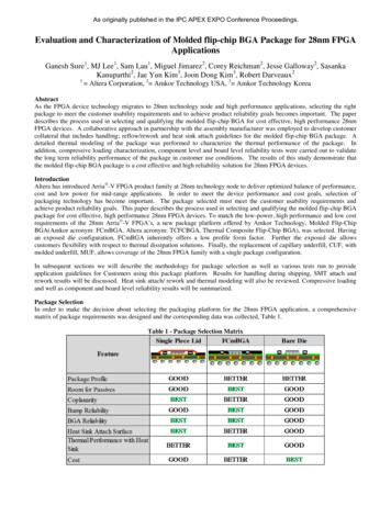
As originally published in the IPC APEX EXPO Conference Proceedings.Evaluation and Characterization of Molded flip-chip BGA Package for 28nm FPGAApplicationsGanesh Sure1, MJ Lee1, Sam Lau1, Miguel Jimarez2, Corey Reichman2, Jesse Galloway2, SasankaKanuparthi2, Jae Yun Kim3, Joon Dong Kim3, Robert Darveaux21 Altera Corporation, 2 Amkor Technology USA, 3 Amkor Technology KoreaAbstractAs the FPGA device technology migrates to 28nm technology node and high performance applications, selecting the rightpackage to meet the customer usability requirements and to achieve product reliability goals becomes important. The paperdescribes the process used in selecting and qualifying the molded flip-chip BGA for cost effective, high performance 28nmFPGA devices. A collaborative approach in partnership with the assembly manufacturer was employed to develop customercollateral that includes handling; reflow/rework and heat sink attach guidelines for the molded flip-chip BGA package. Adetailed thermal modeling of the package was performed to characterize the thermal performance of the package. Inaddition, compressive loading characterization, component level and board level reliability tests were carried out to validatethe long term reliability performance of the package in customer use conditions. The results of this study demonstrate thatthe molded flip-chip BGA package is a cost effective and high reliability solution for 28nm FPGA devices.IntroductionAltera has introduced Arria -V FPGA product family at 28nm technology node to deliver optimized balance of performance,cost and low power for mid-range applications. In order to meet the device performance and cost goals, selection ofpackaging technology has become important. The package selected must meet the customer usability requirements andachieve product reliability goals. This paper describes the process used in selecting and qualifying the molded flip-chip BGApackage for cost effective, high performance 28nm FPGA devices. To match the low-power, high performance and low costrequirements of the 28nm Arria -V FPGA’s, a new package platform offered by Amkor Technology, Molded Flip-ChipBGA(Amkor acronym: FCmBGA, Altera acronym: TCFCBGA, Thermal Composite Flip-Chip BGA), was selected. Havingan exposed die configuration, FCmBGA inherently offers a low profile form factor. Further the exposed die allowscustomers flexibility with respect to thermal dissipation solutions. Finally, the replacement of capillary underfill, CUF, withmolded underfill, MUF, allows coverage of the 28nm FPGA family with a single package configuration.In subsequent sections we will describe the methodology for package selection as well as various tests run to provideapplication guidelines for Customers using this package platform. Results for handling during shipping, SMT attach andrework results will be discussed. Heat sink attach/ rework and thermal modeling will also be reviewed. Compressive loadingand well as component and board level reliability results will be summarized.Package SelectionIn order to make the decision about selecting the packaging platform for the 28nm FPGA application, a comprehensivematrix of package requirements was designed and the corresponding data was collected, Table 1.Table 1 - Package Selection Matrix
Package profile is an important consideration, especially as more applications require thin form factors. Both FCmBGA andBare Die packages offer thinner package profile form factor than a single piece lid package, however, as the package getsthinner Bare Die packages are limited on body size and die size. This is due to the Coplanarity requirement. FCmBGA addsadditional support to the die by coupling the MUF to the substrate. This in turn helps control package warpage/Coplanarityand allows for thinner larger packages with larger die. Another gain from the molding compound around die is the packagerobustness compared to the bare die format. This advantage offers many benefits during component handling such asshipping, electrical test, board mounting, rework and heatsink attach. FCmBGA package is advantageous from the point ofview of 28nm FPGA family coverage. Typically a range of die and body sizes are deployed with each new FPGA family.With FCmBGA package, one package type can cover the entire family. Another benefit of FCmBGA over single piece lidand Bare Die is keep out zones, KOZ, requirements. Both single piece lid and Bare Die packages use Capillary Underfill,CUF. CUF requires 2 to 3 mm KOZ between the die and on board passives. This is to prevent partial filling of the on boardpassive solder joints by the CUF, which can lead to solder joint fracture during temperature cycle condition B testing [1].FCmBGA uses molded Underfill, MUF to encapsulate the on board passives and around the die. Thus, the KOZ forFCmBGA package is less restrictive, 0.6mm.The FCmBGA mold cap is designed to be below the attached die height. This allows the thinnest bond line thickness, BLT,and thus the best thermal performance. Work was done with several commercially available heat sinks and TIM II materialsto illustrate how heat sinks can be attached to FCmBGA. Rework of the heat sink was also performed to demonstrate theruggedness of the molded package. Thermal performance was evaluated through FEM modeling.Like with any new package platform, demonstrating that the package meets the customer reliability requirements isimportant. The industry standard component level and board level reliability tests were run to compare the FCmBGAperformance to single piece lid and Bare Die control packages. The package performed well in direct head to headcomparisons.Collaboration to Develop Customer CollateralWith selection of new package type for the 28nm FPGA product family, it was essential to develop customer collateral toensure that the package meets the customer usability requirements. The objective of customer collateral is to provide theguidance to the customers for component handling, board level assembly and rework and develop the heatsink attach andrework process. We collaborated to develop the customer collateral by running joint evaluations on the test vehiclesassembled in the FCmBGA package. Additionally, accelerated component level and board level reliability testing was run toverify the package integrity in the customer use conditions.Selection of Test VehiclesIn order to evaluate and characterize the FCmBGA package ahead of 28nm FPGA product release, test vehicles wererequired to be selected for evaluations. The criterion for the test vehicle selection was that the die size and package size of thetest vehicle should be closer to the largest die/package size combination for the 28nm FPGA family.After reviewing the number of test vehicles available for testing, a 90nm FPGA device was selected for assembly process,handling guidelines, heatsink attach, mechanical characterization and component level reliability tests. A full stack 40nmdaisy chain test vehicle was selected for board reliability testing. The details of the test vehicles are outlined table 2.Table 2. Characterization Test Vehicle DetailsDeviceTest Vehicle - 1Test Vehicle - 2Full Stack 40nm Daisy Chain90nm Altera FPGABump Pitch22 x 19 mm170mm19.24 x 22.17 mm2225mmBump AlloyEutectic (Sn/Pb)Eutectic (Sn/Pb)PackageF1681 FCmBGAF1508 FCmBGADie Size2Assembly42.5x42.5 mmAmkor40x40 mm2AmkorRel TestAlteraAlteraPackage Size2To carry out the board level characterization experiments, a development board representing typical customer assembly boardwas selected. The PCB was designed per IPC-9701 guidelines(2) with 330mmx114mm size, 2.3mm thickness, 8 layer stack upboard as shown in figure 1.
Figure 1. Assembly and Characterization Development BoardFCmBGA Handling Characterization (Tray Drop Test)FCmBGA packages do not require a tray design different than those already available for standard FCBGA bare die (lidless)packages. In fact, the same tray can be often used for an equivalent bare die and FCmBGA package since both packages arelidless and have roughly the same height due to identical package stack ups (though coplanarity is likely lower with aFCmBGA style package). The FCmBGA mold cap is below the die so it will not interfere with a standard JEDEC style traydesign. In the below work, FCmBGA packages were tested for integrity after dropping them in bundled trays. After testing,both package and trays were inspected for damage. Three packages with three different body sizes were tested: 31, 35 and40mm packages were tested. All packages shared the same die size.Test ProcedureFive trays were fully populated with packages and a sixth tray was added as a cover tray. All trays were banded together threetimes with a standard polypropylene band, bagged in an antistatic band, and then boxed. The box was then dropped from aheight of 120cm. The packages and trays were inspected before and after tray drop. The results of the tray drop tests aresummarized in table 3. The visual inspection of the devices after tray drop testing showed no defects, as shown in figures 2aand 2b.Tray Drop Test ResultsTable 3. Tray Drop Test Summary and ResultsBody SizeDie SizePackagePackage Type(mm)(mm)Damage31FCmBGA354019 x 14TrayDamage0/1180/60/1200/60/1050/6Figure 2a and 2b – Top (left) and bottom side (right) of package after the tray drop testSMT Reflow CharacterizationThe SMT reflow characterization experiments conducted at a preferred SMT sub-contractor showed that the FCmBGApackage follows the same SMT practices of single piece lid and Bare Die packages. The same PCB designs are used.Typical surface finishes e.g. organic solder preservative, OSP with eutectic or lead free solder paste may be used.
Like with other flip chip packages a proper thermal profile is required to achieve good BGA balls collapse. Calibratedthermocouples should be used to instrument a reflow profile board and use it to develop an optimized thermal profile of thepackage on board.Figure 3 shows the typical reflow profile used for assembling the FCmBGA on the PCB. The comparison of the reflowprofiles for FCmBGA and the lidded Flip-Chip BGA (Single Piece Lid SPL) package shows that the reflow profiles are quitesimilar and fall within the range of reflow parameters defined in table 5-2 of JEDEC standard J-STD-020[3].Figure 3. Reflow profiles of FCmBGA vs lidded-FCBGAAfter the assembly process was completed, the mounted devices were inspected to verify solder joint integrity. Visualinspection of the solder joints along the package edge and corners showed well formed solder joints. One device was crosssectioned along the package edge to determine the shape and the size of the solder joints formed during SMT. Figure 4 showsthat the solder joints have consistent solder joint shape across the package edge and the center.473um681umPackage Corner Left448um449um736um747umPackage CenterPackage Corner RightFigure 4. FCmBGA solder joints after SMT reflow.SMTReworkCharacterizationLocalized SMT rework of BGA components is typically performed by customers to replace defective parts or upgrade thedevice to latest version. Localized attach of FCmBGA packages is possible with industry standard BGA Rework machines.Like with SMT attach, a profile board with properly attached calibrated thermocouples is required to develop an optimizedreflow profile.The experiments conducted to develop the localized attach reflow profile showed that the reflow parameters were well withthe parameters as defined in JEDEC standard J-STD-020. However, when compared with the lidded FCBGA, one significantdifference was found. Since the FCmBGA package has exposed die surrounded by the mold cap, the heat transfer from thetop heater through the package to the solder joints is uneven. Consequently, the ball collapse along the periphery of thepackage is difficult if only the top heater is used. However, the uneven heat transfer from the top of the package can becompensated by increasing the heat from the bottom heater of the rework machine. With optimized top and bottom heatersettings, an optimized reflow profile for localized attach of FCmBGA package was developed in this study.The devices attached with localized reflow process were visually inspected along the package edge and corners. The visualinspection shows well formed solder joints.One device was cross-sectioned along the package edge to determine the shape and the size of the solder joints formed duringlocalized reflow. Figure 5 shows that the solder joints have consistent solder joint shape across the package edge and thepackage center.
Package Corner LeftPackage CenterPackage Corner RightFigure 5. FCmBGA solder joints after localized attach.Heat Sink Attach and ReworkThe process of attaching a heat sink to the FCmBGA package and subsequently removing the heat sink (to rework the board)is identical to that of a standard bare die or lidded FCBGA package. In this characterization work, heat sinks were attachedusing two different thermal interface materials (TIMs): Double sided thermal tape and thermally conductive epoxy. Sixpackages were evaluated for each thermal interface material. After attach and removal steps were completed, visual and SATinspection were used to inspect for damage to the die or delamination at the passivation or EMC layers. Results show that theheat sink can be attached and removed without damage to the package or die. In the FCmBGA package, the mold compoundaround the die offers additional surface area for increased adhesion and thermal conduction and no die chipping was observedin our evaluation.Heat Sink Removal with Double Sided Thermal TapeThis particular adhesive tape is a popular double-sided thermally conductive adhesive tape. It is rates as reworkable by thesupplier. Six heat sinks were attached and removed using the supplier’s recommended method. All units were inspected withSAT imaging before and after testing. No failures or changes in package quality were detected. Figure 6 shows the processflow and the images of each process step during heat sink rework.Insert razor bladebetween the componentand the heatsinkInsert blade between HS &componentSlowly exert upwardspressure on theheatsink and lift theheatsink and removeHS separating from componentafter twisting with spatulaRemove remainingadhesive from thepackage by applyingIPA and wiping away.Remaining adhesive after HS removalcan be removed with IPAFigure 6. Thermal tape rework process flowHeat Sink Removal with Thermally Conductive EpoxyThis TIM is a thermally conductive epoxy material. The heat sink attach and the removal process was found to be identical tothe lidded FCBGA package. Figure 7 shows the process flow and the images of each process step during heatsink rework.
After separation cured residual 315material remains on the die315 Material was removed cleanly bycarefully wiping with a razor bladeFigure 7. Thermal epoxy rework process flowThermal ModelingDetailed thermal modeling of various flip-chip packaging options was performed using commercially available CFD tool.The analysis was performed to compare the thermal performance of the FCmBGA with bare die FCBGA and single-piece-lidFCBGA (FCLBGA). The package configurations are depicted in the Figure 8 below.Bare-die FCBGAMold cap 50 µmbelow dieFCmBGA0.5 mm Copper LidTIM-ILidded FCBGAFigure 8. Flip-chip package configurations considered in this work
The package construction details used for the simulations are outlined in the below Table 4. The packages were mounted ontoa JEDEC 1S2P board and the simulation boundary was assumed to be a JEDEC still air chamber. Also, the package topsurface was interfaced with a thin sheet of Aluminum (100 x 100 x 1 mm 3) using a TIM-II material (0.5C-in2/W thermalimpedance). The simulation results are shown below in Table 5.Table 4. Package construction detailsPackage Construction DetailsBody (mm)40Die Size (mm)16 x 20 x 0.786Substrate Construction2-2-2Cu Lid thickness for FCLBGA (mm)PackageBare Die FCBGAFCmBGAFCLBGA0.5Table 5. Thermal simulation results summaryTIM-II MaterialMold /W)N/A5.830.75.701.5140.5 C*in 2 /W5.6935.66N/A5.24As seen from the above results, under the conditions assumed in this work, FCmBGA package thermal performance isslightly better than the bare-die package, but still not comparable to the FCLBGA package performance. The θja of theFCmBGA package was about 9% higher than that of FCLBGA. Also, thermally enhanced mold compounds did not have asignificant impact on improving (lowering θ ja) the FCmBGA package thermal performance. It is important to note that thesimulation trends presented here are representative of the particular system thermal solution (TIM-II Aluminum sheet)chosen in this work. The choice of TIM-II and the external heatsink significantly impact the overall package/system thermalperformance. Detailed thermal measurements comparing the thermal performance of FCmBGA with FCLBGA are presentedin the paper by Galloway et al.[4].Compressive Loading CharacterizationTo verify package integrity, three FCmBGA units were surface mounted then tested in compression at 1480N (106 PSI) for aduration of 15 minutes at room temperature using an Instron mechanical tester. The test vehicles were 40mm packages witha 22 x 19mm die, surface mounted to a 2.3mm thick standard JEDEC style board. The acceptance criteria were thefollowing: No damage to the die (either chip out or cracking), No damage to the mold compound (specifically cracking) andno BGA deformation leading to BGA shorting.Compression Load Test SetupTo assure equal loading across the package, a thick steel fixture was placed between the crosshead and package topside.Double sided thermal tape was applied between the package and steel fixture to further promote equal distribution ofcompressive stress, as shown in figure 9.Figure 9 – Photo of the compression test setup
Compression Test ResultsTable 6. Compression Test Summary and ResultsInspection LocationDie SurfaceInspection MethodDwell Time Sample Size1500 N15 minutesResultSAT and VisualDie Active LayersSATEMC to PassivationSATEMC to PackageSATBGA'sForce3PassX-RAY/VisualNo damage to the test vehicles were detected using the inspection methods listed in table 6. Visual inspection was carried outeither with a microscope or an ERSA scope for BGA inspection. The SAT inspection areas include: The die surface, dieactive layers, the EMC adhesion to the passivation, the EMC adhesion to the package under the die as well as the die surface.Figure 10. XRAY of the BGAs after compressive loading shows no signs of shortingFigure 11. Cross section of a sample confirmsthere is no shorting after compressive loading.Additionally, all BGAs of all samples were inspected X-ray imaging(Figure 10). No anomalies were detected between theBGA solder balls. No measureable differences were observed as a result of the compressive loading. For furtherconfirmation, a unit was cross sectioned to the bump and BGA plane (Figure 11). BGA solder balls were confirmed not tohave been shorted together or significantly deformed.Even though the compression test results show that the package can withstand one time application of compressive force upto 1480N, it is recommended that the customers follow heatsink manufacturer’s recommendations for application ofcompressive force for heatsink attach.Component and Board Level ReliabilityThe 28nm FCmBGA devices were subjected to component level and board level reliability test to ensure that package meetsour package level and second level reliability requirements. We has defined the reliability test plan[5] in conformance withthe industry standards defined by JEDEC and IPC organizations. A 28nm FPGA device was used to perform the componentlevel reliability tests and a full stack daisy chain test vehicle was used for the board level reliability tests.The FCmBGA packages were subjected to preconditioning at MSL3 level and a reflow cycle at 260 oC to simulate thecomponent assembly conditions. The devices were electrically tested at intermediate readout points to detect early failures.The parts subjected to board level temperature cycle were continuously monitored to check resistance changes in the daisychains during temperature cycling. Table 7 summarizes the results of the component level and the board level reliability tests.
Table 7. 28nm FPGA Reliability Test ResultsDevicePackageSize(mmxmm)Die Size(mmxmm)Pin count Solder BallMSLReflow TempCNumber oflotsSampleSize/lotReliability Test ResultsTemp Cycle Condition B -55/125 o C(Cycles)33020050070010000/900/900/900/90Bake at 150 o C (Hrs)3Altera 28nmFPGA Device254816850010000/750/750/750/75Unbiased HAST 130 o C, 85% RH (Hrs)35x3518.8x141152Pb-free3260963300/90Lifetest 1.2xVcc, Tj 125 o C (Hrs)32420050010000/720/720/72Temp Humidity Biased 85 oC/85% RH (Hrs)33050010000/900/90Temp Cycle Condition B -55/125 o C(Cycles)3Altera 28nmFPGA Device3020050070010000/900/900/900/90Unbiased HAST 130 o C, 85% RH (Hrs)40x4018.8x141517Pb-free3260963300/90Temp Humidity Biased 85 o C/85% RH (Hrs)33050010000/900/90Board Level Temp Cycle (0-100 o C)Daisy Chain TV42.5x42.5Daisy Chain TV(w/HS)22x181681Pb-freeN/A260# of cycles completed# of Failures13035000/3011035000/10The results of the component and board level reliability tests show that the 28nm FPGA in the FCmBGA package meets theindustry standard reliability test requirements. To confirm that there were no latent defects in the package after the reliabilitytests, detailed construction analysis was performed to check the condition of the bumps, substrate and the die. Theconstruction analysis showed no defects in the substrate, Silicon low dielectric layers and the bumps.ConclusionsOur joint collaboration has resulted in the developing the valuable customer collateral for the FCmBGA package selected for28nm FPGA device family. The customer usability of the FCmBGA package is shown to be equivalent to the lidded flip-chipBGA package while offering advantages of a low profile package. The reliability tests show that the 28nm FPGA device inFCmBGA package meets the component and board level reliability requirements in compliance with the IPC and JEDECstandards. The results of this collaborative study show that the FCmBGA package offers advantages of high performance andlow cost essential for the 28nm FPGA product family.AcknowledgementsWe would like thank to the Altera and Amkor management for their support for this study. Our special thanks to VadaliMahadev, John Xie, Yuan Li, KB Lim, PB Lam from Altera and Mike Young from Betatron for their valuable contributions.References[1]. Islam, etal. “Molded Flip Chip – FCMBGA”, International Conference and Exhibition on Device PackagingMarch 17-20, 2008 Scottsdale, Arizona.[2]. IPC-9701A, “Performance test methods and qualification requirements for surface mount solder f[3]. IPC/JEDEC Standard J-STD-020, Moisture/Reflow Sensitivity Classification for Nonhermetic Solid State Surface files/docs/JSTD020D-01.pdf[4]. J. Galloway, S. Kanuparthi and Q. Wan “Thermal Performance of FC MBGA: Exposed Molded Die Compared to LiddedPackage,” In Proceedings of the 27th Semiconductor Thermal Measurement and Management Symposium (SEMI-THERM),IEEE, San Jose, March 20-24, pp. 181-186, 2011.[5] Altera Reliability Report 53, Q2 2102, http://www.altera.com/literature/rr/rr.pdf
This paper describes the process used in selecting and qualifying the molded flip-chip BGA package for cost effective, high performance 28nm FPGA devices. To match the low-power, high performance and low cost requirements of the 28nm Arria -V FPGA's, a new package platform offered by Amkor Technology, Molded Flip-Chip