Transcription
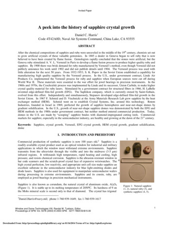
Invited PaperA peek into the history of sapphire crystal growthDaniel C. Harris*Code 4T42A0D, Naval Air Systems Command, China Lake, CA 93555ABSTRACTAfter the chemical compositions of sapphire and ruby were unraveled in the middle of the 19th century, chemists set outto grow artificial crystals of these valuable gemstones. In 1885 a dealer in Geneva began to sell ruby that is nowbelieved to have been created by flame fusion. Gemologists rapidly concluded that the stones were artificial, but theGeneva ruby stimulated A. V. L. Verneuil in Paris to develop a flame fusion process to produce higher quality ruby andsapphire. By 1900 there was brisk demand for ruby manufactured by Verneuil’s method, even though Verneuil did notpublicly announce his work until 1902 and did not publish details until 1904. The Verneuil process was used withlittle alteration for the next 50 years. From 1932-1953, S. K. Popov in the Soviet Union established a capability formanufacturing high quality sapphire by the Verneuil process. In the U.S., under government contract, Linde AirProducts Co. implemented the Verneuil process for ruby and sapphire when European sources were cut off duringWorld War II. These materials were essential to the war effort for jewel bearings in precision instruments. In the1960s and 1970s, the Czochralski process was implemented by Linde and its successor, Union Carbide, to make highercrystal quality material for ruby lasers. Stimulated by a government contract for structural fibers in 1966, H. LaBelleinvented edge-defined film-fed growth (EFG). The Saphikon company, which is currently owned by Saint-Gobain,evolved from this effort. Independently and simultaneously, Stepanov developed edge-defined film-fed growth in theSoviet Union. In 1967 F. Schmid and D. Viechnicki at the Army Materials Research Lab grew sapphire by the heatexchanger method (HEM). Schmid went on to establish Crystal Systems, Inc. around this technology. RotemIndustries, founded in Israel in 1969, perfected the growth of sapphire hemispheres and near-net-shape domes bygradient solidification. In the U.S., growth of near-net-shape sapphire domes was demonstrated by both the EFG andHEM methods in the 1980s under government contract, but neither method entered commercial production. Today,domes in the U.S. are made by “scooping” sapphire boules with diamond-impregnated cutting tools. Commercialmarkets for sapphire, especially in the semiconductor industry, are healthy and growing at the dawn of the 21st century.Keywords: Sapphire, crystal growth, Verneuil, EFG crystal growth, HEM crystal growth, gradient solidification,dome1. INTRODUCTION AND PREHISTORYCommercial production of synthetic sapphire is now 100 years old.1 Sapphire is areadily available crystal product used as an optical window for industrial and militaryapplications in which the window must withstand extreme environments. Sapphiretransmits from the ultraviolet through the visible and into the midwave (3-5 µm)infrared regions. It withstands high temperature, rapid heating and cooling, highpressure, and resists chemical corrosion. Sapphire is the abrasion-resistant window inbar code scanners and the scratch-proof crystal face of expensive wristwatches. The 4high crystal perfection, low reactivity, and appropriate unit cell size make sapphire anexcellent substrate in the semiconductor industry for blue light-emitting diodes anddiode lasers. Sapphire is also used for equipment to manipulate semiconductor wafersduring processing in extreme environments. Sapphire and its cousin, ruby, are 5employed as jewel bearings in precision mechanical instruments.Sapphire is also known as corundum, the natural crystal of aluminum oxide, Al2O3(Figure 1). It is stable up to its melting temperature of 2050ºC. Its hardness of 9 onthe Mohs mineral scale is second only to that of diamond. The crystal has trigonal*Daniel.Harris@navy.mil;123Figure 1: Natural sapphire(1, 2), natural ruby (3), andsynthetic sapphire (4, 5).phone 1-760-939-1649; fax 1-760-939-1617Window and Dome Technologies VIII, Randal W. Tustison, Editor,Proceedings of SPIE Vol. 5078 (2003) 2003 SPIE · 0277-786X/03/ 15.00Downloaded From: http://proceedings.spiedigitallibrary.org/ on 01/16/2014 Terms of Use: http://spiedl.org/terms1
symmetry. The 3-fold symmetry axis, designated c, is also called the optical axis. Two-fold symmetry axes designateda and m are found perpendicular to the 3-fold axis. Pure corundum is clear and colorless. Natural sapphire has avariety of colors. Blue sapphire contains iron and titanium impurities whose charge transfer transition (Fe2 ,Ti4 Fe3 ,Ti3 ) absorbs red light and imparts blue color to the crystal.2 The red color of ruby comes from Cr3 impurities incorundum, which gives rise to electronic transitions that absorb visible light.Early in the 19th century, it was thought that sapphire and ruby were oxides of aluminum and silicon.1 In 1817, J. L.Gay-Lussac found that pure aluminum oxide (also called alumina) could be prepared by thermal decomposition ofammonium alum, (NH4)Al(SO4)2 12H2O. Alumina prepared by this route remains as the raw material for sapphiretoday. In 1840 H. Rose showed that silicon observed in sapphire was an impurity introduced from the agate mortarsused to grind sapphire for chemical analysis. Once the true composition of sapphire was known, many chemists soughtto make the valuable crystal. In the period 1837-1840, H. Gaudin conducted noteworthy investigations. He used atorch to fuse alumina prepared from ammonium alum to prepare small hexagonal platelets of corundum. Mixing alumwith chromium salts prior to fusion produced small, strained, hard red particles whose density was less than that ofnatural ruby because of trapped gas. Gaudin believed he had made a glass, but modern work suggests that he madecrystalline ruby.1 In 1851, H. Senarmont made microscopic rhombohedral crystals by heating solutions of aluminumchloride to over 350ºC in sealed tubes. In 1848, J. J. Ebelman prepared ruby by fusing alumina and boric acid withchromium oxide. Ebelman and F. Parmantier prepared crystals from alumina dissolved in fused salts at hightemperature. Other investigations were carried out by Boettger, Bruhns, Brun, Debray, Deville, Caron, Daubré,Doelter, Elsner, Friedel, Grandeau, Hautefeuille, Houdard, Loyer, Mallet, Medanich, Meunier, Moissan, Morozewicz,Oetling, Perrey, Schuch, and Weinschenk.1,3,4 None of this work produced more than microscopic crystals.More successful investigations were led by EdmondFrémy (1814-1894) at the Museum of Natural History inParis.1 Frémy and his assistant, Charles Feil, publisheda paper in 1877 in which they obtained small, clear, redruby crystals. Fireclay crucibles with 20-kg chargeswere held at red heat for periods up to 20 days. Leadoxide (Pb3O4) was converted to lead aluminate, whichreacted with silica to give lead silicate plus corundumcrystals. Ruby was obtained by adding 2-3 wt%potassium dichromate to the reaction. After Feil died in1876, Frémy’s new assistant was Auguste V. L.Verneuil (1856-1913), who had applied to work withFrémy at the age of 17. Clear ruby crystals up to 3 mmin diameter and 0.3 carat in mass (1 carat 0.2 grams)were grown from alumina in a potassiumhydroxide/barium fluoride flux in a ceramic crucible at1500ºC. In unsuccessful attempts to increase the size ofthe ruby crystals, flux growth was scaled up at theSaint-Gobain glass factory and then in 50-liter cruciblesat the Appert glass factory. Although Frémy thought hewas crystallizing alumina from the flux, Kurt Nassau1suggests that alumina and barium fluoride give gaseousaluminum fluoride. Aluminum fluoride reacts withwater vapor that diffuses through the porous crucible togive alumina, which crystallizes in many locations withlittle chance to grow into larger crystals. Frémysummarized his investigations in a book in 1891.5 Heretired in 1892 and died in 1894. Figure 2, reproducedfrom Nassau,6 was taken from Frémy’s book.2Figure 2: Crystal growth storage cabinet from Frémy’s lab.5,6Proc. of SPIE Vol. 5078Downloaded From: http://proceedings.spiedigitallibrary.org/ on 01/16/2014 Terms of Use: http://spiedl.org/terms
2. FLAME FUSION AND THE VERNEUIL PROCESSIn 1885 rubies selling for 1000-2500 per carat from an unknown source appeared in Geneva and were purported to benatural gems.1 Investigation of the crystals at the Sorbonne in Paris and at Tiffany in New York found microscopic gasbubbles suggestive of a high-temperature synthetic process. The French Syndicate of Diamonds and Precious Stonesruled that the crystals had to be marketed as “artificial,” which dropped their price to 25-40 per carat. Moderninvestigation of “Geneva” rubies by Nassau suggests a 3-stage flame fusion synthetic process.1 In the first stage,alumina plus a chromium salt are fused on a ceramic support to form a tiny crystalline ball. The ball is then turnedupside down and growth of a larger crystalline ball is continued by adding fresh material to the flame. The final stageappears to require 2 torches to enlarge the growing crystal to its final dimensions. The proposed mechanism issupported by 2 discontinuities in chromium concentration inside “Geneva” rubies. One of the people who examined“Geneva” ruby in 1886 was the mineralogist, P. M. E. Jannettaz at the Museum of Natural History in Paris. Heconcluded that fusion was involved in the creation of the “Geneva” ruby and he discussed his findings with hiscolleague, Verneuil.While working with Frémy, Verneuil had earned his bachelor, masters, and doctoral degrees. When Frémy retired in1892, Verneuil became professor of applied chemistry at the Museum of Natural History in Paris. In 1886, followinghis introduction to the “Geneva” ruby by Jannettaz, Verneuil and G. A. Terreil used a hydrogen-oxygen torch to fusealumina powder with some added chromium salt. They obtained tiny particles, which Jannettaz identified as ruby.From this experiment, Verneuil began in earnest in 1888 to develop flame fusion growth of ruby.Working with his student, Marc Paquier, Verneuil developed the flame fusion process well enough to write the detailsin a sealed report that he deposited at the Paris Academy of Science in 1891. After further improvement in decreasinggrowth stress, Verneuil deposited a second sealed document at the Academy of Science in 1892. Marc Paquier,presumably the same person who assisted Verneuil, displayed ruby crystals at the World Fair in Paris in 1900. Thecrystals, for which there was brisk demand, appear to have been made by the Verneuil process, not the Geneva process,and commercial production had already begun by 1900. In 1902, Verneuil announced that he had developed a flamefusion process for making ruby and he published full details in 1904.7Figure 3 is taken from one of Verneuil’s two U.S. patents. To make feed powder, ammonium aluminum sulfate andammonium chromium sulfate were each recrystallized 4-5 times and a mixture of the two was calcined at 1000-1200ºCto give a mixture of the oxides. Ground powder was placed in container B in Figure 3 and delivered into tube K by thetapping hammer D. Oxygen was also delivered through tube K and illuminating gas was delivered through tube S.The flame burned inside the ceramic muffle insulator M whose inside diameter was 25 mm and whose inside heightwas 105 mm. An alumina pedestal L held by a platinum tube could be lowered away from the flame by crank P as thecrystal grew on the pedestal. A mica window covered by a steel shutter, neither of which is shown in Figure 3, enabledthe operator to view the growing crystal inside the muffle.The crystal growth process described in Verneuil’s patent is shown in Figure 4. Powder falling through the flame washeated just below its melting point. The initial powder built up a conical pile in which the hot particles sinteredtogether to make a rigid “sinter cone.” The upper tip of the cone became molten when the cone got sharp enough.Fresh powder landing on the molten ball would melt and enlarge the crystal. Only the uppermost skin of the growingcrystal was molten. As the crystal grew in a vertical direction, the pedestal was lowered to keep the top of the crystal atthe correct location in the flame. Flame temperature during crystal growth was regulated by controlling the flow ofoxygen. At the end of a growth run, the flame was shut and, if there was not too much strain, the crystal would notshatter. Even so, crystals had so much strain that a light tap at the end would split the crystal lengthwise into twohalves. A typical growth time of 2 hours produced a 15 carat cylinder with a diameter of 6 mm and length of 25 mm.In 1909 Verneuil was appointed chief chemist at the Paris laboratory of the New York jewelry company, L. Heller andSons. His charge was to grow blue sapphire for jewelry. The origin of the blue color was not known until chemicalanalyses by Verneuil showed that natural blue sapphire always contained both iron and titanium. Armed with thisknowledge, Verneuil was able to grow deliberately doped blue sapphire. The Paris laboratory was closed in 1911 withthe successful completion of the project.Proc. of SPIE Vol. 5078Downloaded From: http://proceedings.spiedigitallibrary.org/ on 01/16/2014 Terms of Use: http://spiedl.org/terms3
Powder feedFigure 3: Diagram of Verneuil’s apparatus for growingsapphire. From U.S. Patent 1,004,505, September 26, 1911.WatercoolingjacketFlame andgrowingcrystalB. container of feed powderD. hammerG. rotating camO. oxygen feed tubeH. illuminating gas feed tubeK inner tube carries oxygenS. outer tube carries illuminating gasM. muffle (insulation) surrounding downward-pointingflameL. ceramic pedestalP. crank for lowering pedestal to keep crystal at correctMechanism to lowercrystal to keepgrowth surface atcorrect elevation inthe flameFigure 4: Method of growingsapphire described inVerneuil’s U.S. Patent1,004,505.Ruby and sapphire manufacturing by the Verneuil process had begun in Europe prior to Verneuil’s publication of1904.1 One of the largest Verneuil operations was that of Industrie de Piérres Scientifiques, Hrand Djévahirdjian inFrance and Switzerland. The company had a room with approximately 100 Verneuil torches operating around 1920.Heller Company had planned to manufacture blue sapphire in the U.S. but found that labor costs were too high tocompete with European manufacturing. Blue sapphire was grown for Heller by Baikovsky Brothers in France.Baikovsky had 3 torches in 1903, 80 in 1914, 400 in 1919, and 1600 torches in 1980. By 1980 there wereapproximately six large Verneuil manufacturers with a total capacity of 109 carats/yr. Most sapphire was cut intojewel bearings for watches and precision instruments. The process of cutting jewels wastes approximately 99% of theas-grown boule.4Proc. of SPIE Vol. 5078Downloaded From: http://proceedings.spiedigitallibrary.org/ on 01/16/2014 Terms of Use: http://spiedl.org/terms
In the Soviet Union, S. K. Popov (1903-1953) began experiments with the Verneuil method in 1932.4 By 1938 he hadproduced a semi-automatic growth apparatus which enabled the manufacturing of long thin rods suitable for makingjewels for watches and instruments. From 1938 until his death, Popov worked at the Institute of Crystallography of theAcademy of Sciences of the USSR. In 1945-50 he improved the equipment for making ruby rods, solving suchproblems as accurate supply of powder and uniform heating of the growing crystal. In 1951-53 he developed a new usefor sapphire as a durable fiber guide in the textile industry. He also devised equipment for bending corundum rods intoshapes. A commentary written by N. N. Sheftal’ in 1959 stated that Popov’s equipment was more advanced than thatof Western Europe and that the crystal quality produced in the Soviet Union was higher than that available elsewhere.43. BIRTH OF THE SAPPHIRE INDUSTRY IN THE UNITED STATESPrior to the publication by Verneuil in 1904, industrial production of ruby began in the town of Hoquiam, Washingtonin the period 1903-1904. The story pieced together by Nassau1 states that two entrepreneurs, Polson and Ninemire,who had accumulated wealth in the lumber industry, hired an assistant of Verneuil to establish a flame fusion facility togrow ruby for jewelry. It was necessary to send boules to New York for cutting and the venture as a whole was noteconomical. The arrival of less expensive Verneuil ruby from Europe ended any hope of American production.There was no further U.S. production of ruby or sapphire until America was cut off from European supplies of jewelbearings in World War II. The U.S. government issued development contracts which led to production by Linde AirProducts Co. in Indiana in 1942. One advantage that Linde had for sapphire production was that Linde was a majorsupplier of industrial gases, including those used for the Verneuil torch. Linde was later acquired by Union CarbideCorp. After the war, the U.S., again, could not compete with Europe for economy in sapphire production. In the late1940s Linde developed a process for making star sapphire and star ruby, which contain needles of titanium dioxide, forjewelry. Another market for sapphire was fiber guides in the textile industry. The Linde plant in Indiana was closed in1974 and Union Carbide’s Linde Crystal Products Division concentrated on Czochralski crystal growth in Californiaand Washington State. In 1999 the Crystal Products Division was acquired by Bicron, a division of the Frenchcompany, Saint-Gobain. In 2000 the division was renamed “Saint-Gobain Crystals and Detectors”.4. INVENTION OF NEW METHODS FOR GROWING SAPPHIREVerneuil’s flame fusion process, perfected in 1892, hardly changed in the 70 years in which it was the only significantcommercial production method for sapphire. There is still demand for Verneuil material at the dawn of the 21stcentury because the method is the least expensive way to make sapphire and ruby whose quality is adequate for manyapplications. However, higher crystal quality demanded by electronic and optical applications, and the need for sizesand shapes that cannot be made by flame fusion, sparked the development of other ways to make sapphire after 1960.IridiumcrucibleA resurgence of interest in ruby arose with the invention of the ruby laser in1960 using a Verneuil boule grown by Union Carbide in 1959. It wasquickly discovered that the optical quality of Verneuil boules was notadequate for lasers. This dilemma led to the development of sapphire growthby the Czochralski method at Union Carbide in the 1960s. In this process,alumina is melted in an iridium crucible in an atmosphere of 98% N2 / 2%O2. A seed crystal is then dipped into the liquid and withdrawn at a rate of6-25 mm/h while rotating at a rate up to 30 rpm. As the seed is withdrawn,alumina from the melt crystallizes onto the seed. The diameter of the boulecould be controlled by the rate of withdrawal of the seed. Boule diameters upto 11 cm could be obtained from a 15-cm-diameter crucible. Saint-Gobain inWashington State and Crystar Research (a division of Johnson Matthey) inVancouver, Canada both produce sapphire today by the Czochralski method.In addition to Czochralski crystal growth, three other methods to growsapphire were introduced in the 1960s. Edge-defined film-fed growth wasdeveloped independently in the U.S and the U.S.S.R. The heat exchanger method was developed in the U.S. andFigure 5: Czochralski crystal growth.Proc. of SPIE Vol. 5078Downloaded From: http://proceedings.spiedigitallibrary.org/ on 01/16/2014 Terms of Use: http://spiedl.org/terms5
gradient solidification was introduced in Israel.Edge-defined film-fed growth (EFG) was invented by Harold LaBelleat Tyler Laboratories in Waltham, Massachusetts and patented in1971. Tyler was a small laboratory that received a contract from theAir Force in 1965 to make fibers for reinforcement of metal matrixcomposites.8,9,10 LaBelle showed that molten alumina could wet thesurface of a molybdenum die which could be used as a wick to delivermolten material to a growing crystal. Figure 6 shows a sapphire seedcrystal in contact with molten alumina at the top of the die. As theFigure 6: Edge-defined Film-fed Growthseed is withdrawn, liquid crystallizes near the interface of the die and(EFG) of sapphire from molybdenum dies.the seed. Dies of different shape can create crystals that match theshape of the die. Fibers would be drawn from a narrow-diameter diewith a hole through the middle. Tubes could be drawn from the die shown at the right in Figure 6. Fibers grown in theAir Force program in 1965-66 were nearly opaque and there was no demand for the product. In the 1980s, EFGgrowth of transparent sapphire optical fibers for high temperature environments was initially funded by the Departmentof Energy. Concurrent with the work of LaBelle in the 1960s, Stepanov independently invented edge-defined film-fedsapphire growth in the Soviet Union.11,12Tyler and other small companies were acquired by a single owner who changed the name to Tyco Laboratories. In1970 Tyco created the Saphikon Division to produce EFG sapphire in Waltham. Around 1979 the Saphikon Divisionmoved to Milford, New Hampshire. In the 1970s and 1980s Saphikon received the bulk of its revenue by licensing theEFG process to companies such as Kyocera, RCA, Corning, and Allied Signal, all of whom saw commercial potentialfor sapphire substrates for the newly developing silicon-on-sapphire electronics technology. In the mid 1980s theowner of Tyco died. With less than two million dollars per year in sapphire revenue at that time, the new ownerunsuccessfully sought a buyer for the Saphikon Division. Eventually he made a deal with LaBelle that was “too good torefuse”. LaBelle purchased Saphikon in 1985 and resold it at a profit in 1987. Saphikon remained independent until2000 when Saint-Gobain purchased the company and the rights to make sheets, rods, tubes, and 3-dimensional shapes.The newly formed, independent company Photran retained exclusive rights to manufacture sapphire fibers.Kyocera in Japan acquired EFG technology from Saphikon and further developed the process. Kyocera sells r-, a-, or cplane sheets up to 20 cm wide x 30 cm long x 0.02-2 cm thick. Kyocera also sells c-axis rods and tubes.The Heat Exchanger Method (HEM) for growing large sapphire boules was invented by Fred Schmid and DennisViechnicki at the Army Materials Research Lab in Watertown, Massachusetts in 1967.13,14 Fresh out of college in theearly 1960s, Schmid worked in manufacturing at the Watertown Arsenal, where he gained experience in the directionalsolidification of metals and with a helium-cooled arc furnace for casting titanium. He then went to graduate school atNortheastern University to earn a masters degree in materials science. Returning to the Watertown Lab in 1967,Schmid set to work with Viechnicki on directional solidification of an alumina melt onto a sapphire seed crystal.The modern implementation of Schmid and Viechnicki’s heat-exchanger method at Crystal Systems in Salem,Massachusetts is shown in Figure 7. A sapphire seed crystal is placed at the bottom of a molybdenum crucible which isthen loaded with pure alumina crackle, a byproduct of the Verneuil process. The furnace is evacuated and resistivelyheated to melt the crackle while keeping the seed just below its melting point by passing helium gas through the heatexchanger beneath the center of the crucible. Heat and vacuum help purify the alumina by vaporizing some impurities.After partial melting of the seed, helium flow is increased to cool the seed and initiate crystallization of alumina ontothe seed. The furnace is held at constant temperature during growth of the crystal, which proceeds out from the seed in3 dimensions. After crystallization is complete, the furnace temperature and the helium flow are decreased and theboule is slowly annealing in situ. The long slow cooldown produces sapphire of the highest crystal quality. Bouleswith a diameter of 34 cm and a mass of 65 kg are routinely produced and boules up to 38 cm have been grown.Single crystals of sapphire were grown in an 18-mm-diameter crucible in 1967 at Watertown. By 1969, after about 50attempts, crack-free sapphire with a diameter of 76 mm was grown. By 1971 the diameter was up to 152 mm. The6Proc. of SPIE Vol. 5078Downloaded From: http://proceedings.spiedigitallibrary.org/ on 01/16/2014 Terms of Use: http://spiedl.org/terms
(a)(b)Figure 7: (a) Furnace used atCrystal Systems to grow sapphireby the Heat Exchanger Method.(b) The first sapphire boulegrown at Watertown in 1967.(c) Production-quality 34-cmdiameter sapphire boule.Courtesy Crystal Systems, Inc.(c)first patent for the process, which was then known as the Schmid-Viechnicki technique, was issued in 1969.By early 1971, Schmid was convinced that the new method was a breakthrough and wanted to find a commercialmarket for the product. He found interest at Inselec and Insaco in obtaining sapphire wafers for silicon-on-sapphireelectronics. Schmid persuaded a sailing buddy and an accountant to invest in creating the company, Crystal Systems,of which Schmid would own 51%. The company was incorporated in August 1971 after Schmid had purchased ascrapped furnace from Raytheon in July. He began refurbishing the furnace in his garage and soon moved theoperation to Shetland Industrial Park in Salem. For the first year of the company, Schmid held his old job atWatertown and worked on the furnace at night. By July 1972 he grew his first 152-mm-diameter boule, from which51-mm cores were drilled for silicon-on-sapphire substrate wafers. In. September 1972 Schmid resigned fromWatertown to devote full attention to Crystal Systems. He hired his first helper (who was “just getting out of highschool”) and his wife handled advertising. First-year sales were less than fifty thousand dollars. Shortly after the firstadvertising went out in 1974, Schmid received a letter from Union Carbide indicating that Crystal Systems wasinfringing on their patent and offering to license Union Carbide technology. This claim led Schmid to clarify thedifference between the processes and to obtain a patent for his technique, whose name he changed to “heat-exchangermethod” because of its unique, controllable heat exchanger.In the mid 1970s Crystal Systems began to hire full-time employees. Schmid developed a fixed-abrasive slicingtechnique using a diamond-impregnated blade or wire to slice wafers from a cylinder with minimal loss of material.The National Aeronautics and Space Administration selected HEM sapphire for use in satellites because of itsextremely low optical scatter. In 1978 the company moved to its current, larger quarters in the same industrial park.In 1979 Crystal Systems received a contract to grow laser-quality ruby in one of the first actions of the government’snew Small Business Innovative Research program.In 1987-89, titanium-doped sapphire for lasers wascommercialized. Military and commercial markets for sapphire expanded greatly in the 1980s. In 1974 CrystalSystems got its first government contract to grow silicon and in 1977 Chandra Khattak at Crystal Systems used theheat-exchanger method to grow crack-free polycrystalline silicon ingots in high purity silica crucibles for the first time.Proc. of SPIE Vol. 5078Downloaded From: http://proceedings.spiedigitallibrary.org/ on 01/16/2014 Terms of Use: http://spiedl.org/terms7
HEM silicon for photovoltaics and equipment for growing silicon are currently major products of Crystal Systems, inaddition to sapphire and crystal slicing equipment. HEM silicon ingots weighing 240 kg with a cross section of 69 69 cm are routinely produced.5. SAPPHIRE DOMESOne of the most demanding applications for an infrared window material is the seeker dome on an infrared-guidedmissile. The dome must withstand stress from very rapid heating and it must survive collisions with raindrops, sandparticles, and insects in the air. Among the infrared-transparent materials available in the 1980s, sapphire was clearlythe most durable with respect to thermal stress and particle impact. However, the cost of growing sapphire was highand the cost of fabricating it into an optically polished hemisphere was even higher. To decrease the cost, thegovernment invested in two efforts to grow near-net-shape domes which would require relatively little machining aftergrowth.One Navy-funded effort at Saphikon ledto a Manufacturing Technology contractin 1989-92. A curved sapphire seedcrystal was placed in contact with acurved slit at the top of a molybdenumdie for EFG growth. The seed was slowlywithdrawn in a path that traced an arc inspace. The result was an as-grown domesuch as that in Figure 8. The sapphire atthe right of the figure could be machinedinto a dome shape. However, the crystalquality was not as high as desired and themanufacturing process was neveroptimized.15,16Figure 8:As-grown EFGsapphireproduced bySaphikon.15,16Another Navy Small Business Innovative Research contract was conducted at Crystal Systems. Work done in the midto late 1980s used the apparatus shown at the left in Figure 9 to grow the near-net-shape domes at the right.17-19 Twohemispheric molybdenum mandrels were inserted into the crucible in which sapphire was grown. After a boule wasgrown and cracked apart, sapphire that crystallized in the volume between the two mandrels had a hemispheric shape.This method suffered from cracks extending into the boule and it was never taken beyond an initial demonstration.Figure 9: Molybdenum apparatus at left was used at Crystal Systems to grow near-net-shape sapphire domes at right.17-19 Photoscourtesy Crystal Systems.8Proc. of SPIE Vol. 5078Downloaded From: http://proceedings.spiedigitallibrary.org/ on 01/16/2014 Terms of Use: http://spiedl.org/terms
Domes were formerly produced from sapphire boules by machining each dome out of a cy
natural ruby because of trapped gas. Gaudin believed he had made a glass, but modern work suggests that he made crystalline ruby.1 In 1851, H. Senarmont made microscopic rhombohedral crystals by heating solutions of aluminum chloride to over 350ºC in sealed tubes. In 1848, J. J. Ebelman prepared ruby by fusing alumina and boric acid with