Transcription
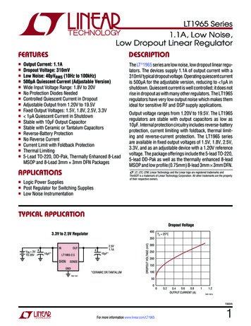
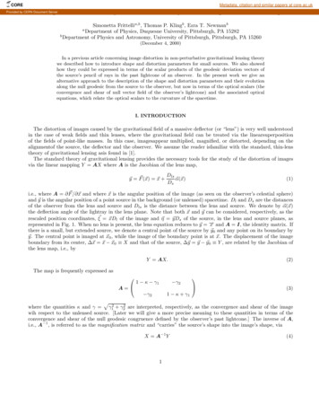
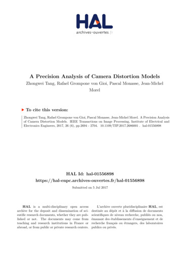
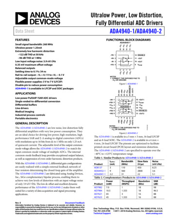
Ultralow Power, Low Distortion,Fully Differential ADC DriversADA4940-1/ADA4940-2Data SheetFEATURESFUNCTIONAL BLOCK DIAGRAMS13 –VS14 –VS16 –VS–FB 112 DISABLE IN 211 –OUT–IN 310 OUT919 –OUT121 –VS120 DISABLE124 IN123 –FB122 –VS1Figure 1. ADA4940-118 OUT117 VOCM116 –VS2–IN1 1 FB1 2 VS1 3ADA4940-2 VS1 415 –VS2NOTES1. CONNECT THE EXPOSED PAD TO–VS OR GROUND.07429-202 OUT2 12 VS2 1013 –OUT2VOCM2 11 IN2 6–IN2 714 DISABLE2 FB2 8 VS2 9–FB2 5GENERAL DESCRIPTIONWith the ADA4940-1/ADA4940-2, differential gain configurationsare easily realized with a simple external feedback network offour resistors determining the closed-loop gain of the amplifier.The ADA4940-1/ADA4940-2 are fabricated using Analog Devices,Inc., SiGe complementary bipolar process, enabling them toachieve very low levels of distortion with an input voltage noiseof only 3.9 nV/ Hz. The low dc offset and excellent dynamicperformance of the ADA4940-1/ADA4940-2 make them wellsuited for a variety of data acquisition and signal processingapplications.08452-001NOTES1. CONNECT THE EXPOSED PAD TO–VS OR GROUND.Low power PulSAR /SAR ADC driversSingle-ended-to-differential conversionDifferential buffersLine driversMedical imagingIndustrial process controlsPortable electronicsThe ADA4940-1/ADA4940-2 are low noise, low distortion fullydifferential amplifiers with very low power consumption. Theyare an ideal choice for driving low power, high resolution, highperformance SAR and Σ-Δ analog-to-digital converters (ADCs)with resolutions up to 16 bits from dc to 1 MHz on only 1.25 mAof quiescent current. The adjustable level of the output commonmode voltage allows the ADA4940-1/ADA4940-2 to match theinput common-mode voltage of multiple ADCs. The internalcommon-mode feedback loop provides exceptional output balance,as well as suppression of even-order harmonic distortion products.VOCM VS 8 VS 7 VS 6 VS 5 FB 4APPLICATIONSRev. E15 –VSADA4940-1Small signal bandwidth: 260 MHzUltralow power 1.25mAExtremely low harmonic distortion 122 dB THD at 50 kHz 96 dB THD at 1 MHzLow input voltage noise: 3.9 nV/ Hz0.35 mV maximum offset voltageBalanced outputsSettling time to 0.1%: 34 nsRail-to-rail output: VS 0.1 V to VS 0.1 VAdjustable output common-mode voltageFlexible power supplies: 3 V to 7 V (LFCSP)Disable pin to reduce power consumptionADA4940-1 is available in LFCSP and SOIC packagesFigure 2. ADA4940-2The ADA4940-1 is available in a 3 mm 3 mm, 16-lead LFCSPand an 8-lead SOIC. The ADA4940-2 is available in a 4 mm 4 mm, 24-lead LFCSP. The pinouts are optimized to facilitateprinted circuit board (PCB) layout and minimize distortion.The ADA4940-1/ADA4940-2 are specified to operate over the 40 C to 125 C temperature range.Table 1. Similar Products to ISUPPLY(mA)392.2Bandwidth(MHz)11056031Slew Rate(V/μs)450280022Noise(nV/ Hz)8.253.65.1Table 2. Complementary Products to solution(Bits)18181616SNR(dB)9896.58888Document FeedbackInformation furnished by Analog Devices is believed to be accurate and reliable. However, noresponsibility is assumed by Analog Devices for its use, nor for any infringements of patents or otherrights of third parties that may result from its use. Specifications subject to change without notice. Nolicense is granted by implication or otherwise under any patent or patent rights of Analog Devices.Trademarks and registered trademarks are the property of their respective owners.One Technology Way, P.O. Box 9106, Norwood, MA 02062-9106, U.S.A.Tel: 781.329.4700 2011–2018 Analog Devices, Inc. All rights reserved.Technical Supportwww.analog.com
ADA4940-1/ADA4940-2Data SheetTABLE OF CONTENTSFeatures . 1Applications Information . 23Applications . 1Analyzing an Application Circuit . 23General Description . 1Setting the Closed-Loop Gain . 23Functional Block Diagrams . 1Estimating the Output Noise Voltage . 23Revision History . 3Impact of Mismatches in the Feedback Networks . 24Specifications. 4Calculating the Input Impedance of an Application Circuit 24VS 5 V. 4Input Common-Mode Voltage Range . 25VS 3 V. 6Input and Output Capacitive AC Coupling . 26Absolute Maximum Ratings . 8Setting the Output Common-Mode Voltage . 26Thermal Resistance . 8DISABLE Pin . 26Maximum Power Dissipation . 8Driving a Capacitive Load. 26ESD Caution . 8Driving a High Precision ADC . 27Pin Configurations and Function Descriptions . 9Layout, Grounding, and Bypassing . 28Typical Performance Characteristics . 11ADA4940-1 LFCSP Example . 28Test Circuits . 20Outline Dimensions . 29Terminology . 21Ordering Guide . 30Definition of Terms . 21Theory of Operation . 22Rev. E Page 2 of 30
Data SheetADA4940-1/ADA4940-2REVISION HISTORY4/2018—Rev. D to Rev. EChanges to Figure 2. 1Changes to Figure 6.10Updated Outline Dimensions .295/2016—Rev. C to Rev. DChanges to Figure 1. 1Deleted Figure 2. 1Added Figure 2; Renumbered Sequentially . 1Updated Outline Dimensions .29Changes to Ordering Guide .309/2013—Rev. B to Rev. CUpdated Outline Dimensions .30Changes to Ordering Guide .313/2012—Rev. A to Rev. BReorganized Layout . UniversalAdded ADA4940-1 8-Lead SOIC Package . UniversalChanges to Features Section, Table 1, and Figure 1; ReplacedFigure 2 . 1Changed VS 2 V(or 5 V) Section to VS 5 V Section . 3Changes to VS 5 V Section and Table 3 . 3Changes to Table 4 and Table 5 . 4Changes to VS 3 V Section and Table 6 . 5Changes to Table 7 and Table 8 . 6Added Figure 5 and Table 12, Renumbered Sequentially . 9Changes to Figure 7, Figure 8, and Figure 9 .10Added Figure 15 and Figure 18; Changes to Figure 13,Figure 14, and Figure 16 .11Changes to Figure 19 and Figure 20 .12Changes to Figure 25, Figure 26, and Figure 27; AddedFigure 28, Figure 29, and Figure 30 .13Changes to Figure 31, Figure 32, Figure 33, Figure 34, Figure 35,and Figure 36 .14Changes to Figure 37, Figure38, Figure 39, and Figure 41 . 15Changes to Figure 49, Figure 50, and Figure 51 . 17Added Figure 55 and Figure 57 . 18Changes to Differential VOS, Differential CMRR, and VOCMCMRR Section . 20Changes to Calculating the Input Impedance of an ApplicationCircuit Section . 23Changes to Figure 71 . 25Changes to Driving a High Precision ADC Section andFigure 73 . 26Changed ADA4940-1 Example Section to ADA4940-1 LFCSPExample Section . 27Changes to Ordering Guide . 2912/2011—Rev. 0 to Rev. AChanges to Features Section, General Description Section, andTable 1 . 1Replaced Figure 1 and Figure 2 . 1Changes to VS 2.5 V (or 5 V) Section and Table 3 . 3Changes to Table 6 . 5Replaced Figure 7, Figure 8, Figure 9, and Figure 10 . 9Replaced Figure 14, Figure 15, and Figure 17 . 10Replaced Figure 24 and Figure 27 . 12Changes to Figure 37 . 14Replaced Figure 43 and Figure 46 . 15Replaced Figure 53 . 18Changes to Estimating the Output Noise Voltage Section, Table 14,Table 15, and Calculating the Input Impedance of an ApplicationCircuit Section . 21Changes to Input Common-Mode Voltage Range Section . 22Changes to Driving a High Precision ADC Section andFigure 65 . 2410/2011—Revision 0: Initial VersionRev. E Page 3 of 30
ADA4940-1/ADA4940-2Data SheetSPECIFICATIONSVS 5 VVOCM midsupply, RF RG 1 kΩ, RL, dm 1 kΩ, TA 25 C, LFCSP package, unless otherwise noted. TMIN to TMAX 40 C to 125 C.(See Figure 61 for the definition of terms.) DIN or –DIN to VOUT, dm PerformanceTable 3.ParameterDYNAMIC PERFORMANCE 3 dB Small Signal Bandwidth 3 dB Large Signal BandwidthBandwidth for 0.1 dB FlatnessSlew RateSettling Time to 0.1%Overdrive Recovery TimeNOISE/HARMONIC PERFORMANCEHD2/HD3IMD3Input Voltage NoiseInput Current NoiseCrosstalkINPUT CHARACTERISTICSInput Offset VoltageInput Offset Voltage DriftInput Bias CurrentInput Bias Current DriftInput Offset CurrentInput Common-Mode Voltage RangeInput ResistanceInput CapacitanceCommon-Mode Rejection Ratio (CMRR)Open-Loop GainOUTPUT CHARACTERISTICSOutput Voltage SwingLinear Output CurrentOutput Balance ErrorTest Conditions/CommentsMinTypMaxUnitVOUT, dm 0.1 V p-p, G 1VOUT, dm 0.1 V p-p, G 2VOUT, dm 0.1 V p-p, G 5VOUT, dm 2 V p-p, G 1VOUT, dm 2 V p-p, G 2VOUT, dm 2 V p-p, G 5VOUT, dm 2 V p-p, G 1 and G 2VOUT, dm 2 V stepVOUT, dm 2 V stepG 2, VIN, dm 6 V p-p, triangle /µsnsnsVOUT, dm 2 V p-p, fC 10 kHzVOUT, dm 2 V p-p, fC 50 kHzVOUT, dm 2 V p-p, fC 50 kHz, G 2VOUT, dm 2 V p-p, fC 1 MHzVOUT, dm 2 V p-p, fC 1 MHz, G 2VOUT, dm 2 V p-p, f1 1.9 MHz, f2 2.1 MHzf 100 kHzf 100 kHzVOUT, dm 2 V p-p, fC 1 MHz 125/ 118 123/ 126 124/ 117 102/ 96 100/–92 993.90.81 110dBcdBcdBcdBcdBcdBcnV/ HzpA/ HzdBVIP VIN VOCM 0 VTMIN to TMAX 0.35 1.6TMIN to TMAX 500DifferentialCommon modeΔVOS, dm/ΔVIN, cm, VIN, cm 1 V dc8691Each single-ended output VS 0.1 to VS 0.1f 1 MHz, RL, dm 22 Ω, SFDR 60 dBcf 1 MHz, ΔVOUT, cm/ΔVOUT, dmRev. E Page 4 of 30 0.061.2 1.1 4.5 50 VS 0.2 to VS 1.23350111999 VS 0.07 to VS 0.0746 65 0.35 500mVµV/ CµAnA/ CnAVkΩMΩpFdBdBV 60mA peakdB
Data SheetADA4940-1/ADA4940-2VOCM to VOUT, cm PerformanceTable 4.ParameterVOCM DYNAMIC PERFORMANCE 3 dB Small Signal Bandwidth 3 dB Large Signal BandwidthSlew RateInput Voltage NoiseGainVOCM CHARACTERISTICSInput Common-Mode Voltage RangeInput ResistanceOffset VoltageInput Offset Voltage DriftInput Bias CurrentCMRRTest Conditions/CommentsVOUT, cm 0.1 V p-pVOUT, cm 1 V p-pVOUT, cm 1 V p-pf
Ultralow Power, Low Distortion, Fully Differential ADC Drivers Data Sheet ADA4940-1/ADA4940-2 Rev. E Document Feedback Information furnished by Analog Devices is believed to be accurate and reliable.