Transcription
Critical Link, LLCwww.CriticalLink.comPROFIBUS Dev Kit5 March 2014FEATURES PROFIBUS Interfaceo Certified by PI Internationalo Real-Time Linux Driverso Electrically Isolated Interfaceo Up to 6Mbaud operation PROFIBUS Support usingo MitySOM-1810 and 1810Fo MityDSP-L138 and L138F Software Included: Real-Time Linux Kernel uBoot User Boot Loader PROFIBUS PRU Image (binary) Slave PROFIBUS Stack(evaluation version)APPLICATIONS: MitySOM1810 and MityDSP-L138Evaluation PROFIBUS Development Process Automation Factory Automation Industrial Automation Embedded Instrumentation Rapid PrototypingDigital Interfaces: RS-232 Serial Interface USB Host Interface USB OTG Interface 10/100 MBit Ethernet Interface Electrically Isolated CAN BusInterface UART Expansion forPROFIBUS/RS-485 Interface DVI Video Interface SD/MMC Card Socket Audio OutputExpansion: 3 50-pin IO Expansion Slots Integrated 3V/ 5V/ 12V PowerSupplyDESCRIPTIONThe PROFIBUS DEVELOPMENT KIT provides all the hardware and software supportfor system designers and developers to evaluate the AM1810 or OMAPL138Microprocessors for PROFIBUS as well as the Critical Link MitySOM-1810 and/orMityDSP-L138 series System on Modules. Included is a MitySOM-1810 module, but thekit is fully compatible with MitySOM-1810 and MityDSP-L138, and MitySOM-1808modules with varying PROFBIUS support. See the compatibility chart below.Module 138FMitySOM-1808MitySOM-1808FPROFIBUS SupportYesYesYesYesNoNo1Downloaded from Arrow.com.RS485 SupportYesYesYesYesYesYesCopyright 2007-2013, Critical Link LLC
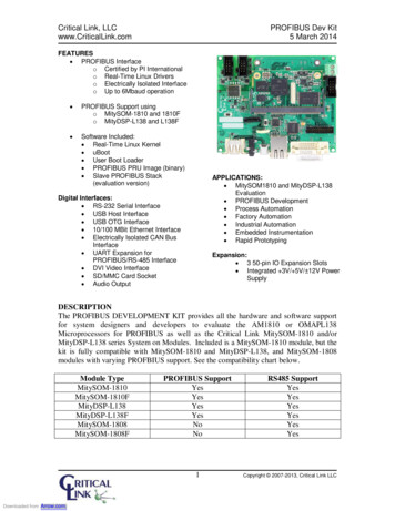
Critical Link, LLCwww.CriticalLink.comPROFIBUS Dev Kit5 March 2014In addition, the PROFIBUS DEVELOPMENT KIT includes on board RS-232, 10/100MBit Ethernet, Universal Serial Bus (USB) Host and USB-On The-Go (OTG)communication interfaces and an Electrically Isolated CAN interface. The single UARTexpansion port allows for the connection of either the PROFIBUS/RS-485 expansionboard (included with the PROFIBUS Development Kit) with 2500V galvanic isolationbarrier or a simple RS232 serial port expansion kit (optional). Integrated Digital VideoInterface (DVI) controller for external display connection with DDC support. Interface toQVGA\WQVGA display via 5 pair LVDS link with additional SPI interface for resistivetouch controller (requires an FPGA based module to be installed), Multi Media Card(MMC) interface, 3 I/O Expansion connectors for custom add-on card and integratedpower supply with 3V/ 5V/ 12V outputs from single 12VDC input.A block diagram of the PROFIBUS DEVELOPMENT KIT is illustrated in Figure 1. Allavailable processor GPIO ports and FPGA I/O lines (if FPGA module is installed) areeither used directly by the PROFIBUS DEVELOPMENT KIT or are routed to the 3 50pin Expansion IO connectors. Control of the on-board interface hardware and connectedExpansion IO cards require proper configuration of the MitySOM / MityDSP ARM,DSP, and FPGA. While not required, it is strongly recommended that the MitySOMsoftware and firmware development kit and supplied API be used to manage theseinterfaces.MitySOM-1810 PROFIBUS Development KitUSB1USB-AConnectorPCMicro-USBConnectorUSB0SD CardMicro-SDConnectorMMCSD 0DiskSATA HeaderSerial10-pin HeaderTRS232ERS232 PHYRJ-45 &MagneticsTLK100Ethernet PHYEthernetProfinetModbus TCPEtherCAT MasterMMCSD0IO10-pin HdrISO1050MCP2515AudioLine Out1/8" stereojackFilterDSD1791Monitor10-pin HdrUART[2]DVITFP410QVGA\WQVGAPanel w/Touchor GPIOLCD / TouchHeader 12VPowerManagementAM1810/OMAP-L138 ARMMicroprocessor for PROFIBUSfromTexas Expansion Header 12x25 2-mmUART[1]I2C [0]MII/MDIO 3.3VIO ser ProgrammableXilinx Spartan 6 FPGAIO Bank 1Expansion Header 32x25 2-mmHID /Thumbdrive 3.3V 12V-12VI/O(available on the MityARM-1810F– Contact Critical Link foradditional information)IO Bank 1Expansion Header 22x25 2-mm 5V ISO 1 (CAN) 5V ISO 2 (RS-485) 5V(Audio) 3.3V-12VFigure 1: PROFIBUS Development Kit Block Diagram2Downloaded from Arrow.com.Copyright 2007-2013, Critical Link LLC
Critical Link, LLCwww.CriticalLink.comPROFIBUS Dev Kit5 March 2014PROFIBUS / UART Expansion Interface DescriptionTexas Instruments Inc. (TI) has integrated PROFIBUS functionality into its AM1810 andOMAP-L138 Sitara ARM microprocessor (MPU). The AM1808 does NOT support thePROFIBUS protocol. The solution utilizes one of the onboard UARTS and connectsthrough the 10-pin UART expansion header on the PROFIBUS DEVELOPMENT KITbase board to the RS485 transceiver on the Expansion Board. This eliminates the need ofan external ASIC or FPGA to support the PROFIBUS interface.Customers using the MitySOM-1810 or MityDSP-L138 in their industrial application cansave cost and reduce design complexity as well as PCB space. Furthermore, the industrialapplication benefits from the low-power architecture of the Sitara ARM MPU and theMitySOM-1810 or MityDSP-L138 platforms from TI and Critical Link.The Sitara ARM MPU PROFIBUS Slave solution has been certified by PROFIBUSInternational (PI).The PROFIBUS real-time frame handler (Fieldbus Data Link or FDL) is encapsulated inthe Programmable Real-Time Unit Subsystem (PRUSS), which is part of the Sitara ARMMPU on-chip peripherals. The PRUSS uses one Universal AsynchronousReceiver/Transmitter (UART) and a timer to generate PROFIBUS-compliant frames. Theindustrial application and the PROFIBUS DP-Protocol (Layer 7) are operated on theARM. The solution is completed with an RS-485 transceiver suitable for harshenvironments, such as TI’s ISO1176 which is found on the PROFIBUS/RS485Expansion Board included with the PROFIBUS Development Kit.The PROFIBUS subsystem uses the PRUs that implement real-time frame handling;PROFIBUS message transmission, frame validation and communication with the ARMprocessor. The PROFIBUS subsystem interfaces with one of the UARTs in the SitaraARM MPU, which is designated for PROFIBUS communication at up to 6Mbaud datarate. The PRU uses interrupts to interact with the ARM where the PROFIBUS stack(Layer 7, DP Protocol) and the industrial application is run. All process data handling likecyclic, acyclic and service access point (SAP) between the PROFIBUS stack on ARMand the PRU is through the internal memory.Additional details about the AM1810 Sitara ARM MPU, available peripherals and theirfeatures are provided in the data sheet at the TI website (www.ti.com/am1810).The UART expansion header allows for a pin-compatible RS232 Expansion Kit that canreplace the PROFIBUS/RS485 Expansion Kit if desired. Please contact Critical Link forfurther details.RS-232 Interface DescriptionThe on-board RS-232 level driver provides standard serial interface at data rates up to115,200 baud. The serial interface is routed to the primary MitySOM / MityDSP serialbootloading port in order to allow remote code download and FLASH upgrades on anattached MitySOM / MityDSP from this connector.3Downloaded from Arrow.com.Copyright 2007-2013, Critical Link LLC
Critical Link, LLCwww.CriticalLink.comPROFIBUS Dev Kit5 March 2014USB Interface DescriptionThe on-board USB interface utilizes dedicated HOST and OTG controllers inside OMAPprocessor. Linux and drivers are available.Ethernet Interface DescriptionThe on-board Ethernet interface features a network PHY capable of running at10/100Mbit including link auto-negotiation and MII/MDIO capability. An industrystandard RJ-45 connector is provided for external connection. This Ethernet interfacemay be used to perform remote code download and FLASH upgrades on an attachedMitySOM or MityDSP module.QVGA/WQVGA LVDS Interface DescriptionThe PROFIBUS DEVELOPMENT KIT provides a flat-ribbon cable low profile interfacefor five Low Voltage Differential Signaling (LVDS) pairs. The interface design isintended to support high speed off board interconnects. In addition to custom userinterfacing, the pairs may be used to interface to a Quarter VGA LCD screen using theMitySOM / MityDSP hardware and software development kit LCD interface libraries andan appropriate daughterboard interface.Off-the-shelf display solutions forQVGA\WQVGA interfaces are provided by Critical Link.The interface can also be customized to support 17 IO lines at 3.3V CMOS/LVTTLsignaling levels based on FPGA configuration.This interface is available only with anFPGA based MitySOM or MityDSP module installed.DVI Interface DescriptionThe PROFIBUS DEVELOPMENT KIT provides a standard DVI interface for externalmonitor connection. Based on CPU utilization, recommended resolution should belimited to VGA (640x480) with 5-6-5 color pallet.CAN Interface DescriptionThe on-board CAN provides a CAN V2.0B compliant interface. This interface ismanaged by a Microchip MCP2515 CAN controller connected to MitySOM / MityDSPvia the SPI1 interface. The galvanic isolation is provided by a dedicated TI ISO1050transceiver. The ISO1050 is powered by an isolated power supply with 1000V* isolationfrom the primary supply.Jumper JP504 can provide dedicated bus termination of 120Ohm. To enable termination,place shorting jumper across JP504.The Electrical interface is provided via J501, 10-pin shrouded header.Linux Driver and API examples are available to support CAN functionality.PROFIBUS / UART Expansion Interface Description (80-000268RI-2 Assemblies)The on-board dedicated UART port provides standard serial interface at data rates up to115,200 baud. The serial interface is routed to the UART2 serial port of MitySOM /4Downloaded from Arrow.com.Copyright 2007-2013, Critical Link LLC
Critical Link, LLCwww.CriticalLink.comPROFIBUS Dev Kit5 March 2014MityDSP. This expansion port can accept either the PROFIBUS/RS485 Expansion Board(Included in the PROFIBUS Development Kit) or an optional RS232 Expansion Boardfrom Critical Link.The port also provides a 5.0V@100mA power via isolated power supply with 1000V*isolation from the primary supply as well as 3.3V@300mA from the main non-isolatedpower supply with a common ground. A single enable GPIO is also routed to this port inaddition to the TX and RX UART signals.The Electrical interface is provided via J504, 10-pin shrouded headerWhen the PROFIBUS/RS485 Expansion Board is used it provides galvanic isolation by adedicated TI ISO1176 transceiver. The ISO1176 is powered by an isolated power supplywith 2500Vrms* isolation from the primary supply. Jumpers on the PROFIBUS/RS485Expansion Board can provide dedicated bus termination.Please see the PROFIBUS/RS485 Expansion Board documentation found /Linux Driver and API examples are available to support PROFIBUS/RS-485functionality.When the RS232 Expansion Board is used the transceiver on it is powered from the 3.3V supply of the Development Kit. It does not provide any /Note: On older PROFIBUS Development Kit base boards, 80-000268RI-1 assemblies,the PROFIBUS/RS485 hardware was installed directly on the base board. The expansionboard was not necessary and therefore not included. Please contact Critical Link fordetails or a previous datasheet if necessary.Real Time Clock BatteryThe PROFIBUS Development Kit includes a battery used to provide power to theinstalled modules real time clock. This battery has been sized to allow for approximately6 months of unpowered time with a module installed until the battery will be depleted.5Downloaded from Arrow.com.Copyright 2007-2013, Critical Link LLC
Critical Link, LLCwww.CriticalLink.comPROFIBUS Dev Kit5 March 2014ABSOLUTE MAXIMUM RATINGSOPERATING CONDITIONSIf Military/Aerospace specified cards arerequired, please contact the Critical LinkSales Office or unit Distributors foravailability and specifications.Ambient TemperatureRangeHumidityMaximum Supply VoltageStorage Temperature Range0 to 70C0 to 95%Noncondensing13.2 V0 to 80CELECTRICAL CHARACTERISTICSSymbolParameterConditionsPower DissipationVSSupply Voltage.ISSupply CurrentReal Time Clock (RTC) BatteryIdrawCurrent draw on battery with Module InstalledTdurationBattery life with Module Installed and no inputpower suppliedNotes:1.TypicalLimitUnits(Limits)12 5%10.45VA106uAMonthsPower Supply load is dependent on Development Kit configuration and utilization.Notes: 1. Expansion card is not attached, 100% DSP/FPGA utilization, RS-232 andEthernet are enabled and active.6Downloaded from Arrow.com.Copyright 2007-2013, Critical Link LLC
Critical Link, LLCwww.CriticalLink.comPROFIBUS Dev Kit5 March 2014ELECTRICAL INTERFACE DESCRIPTIONInput PowerThe PROFIBUS DEVELOPMENT KIT power interface, J600, requires a single 12Voltpower supply.Table 1: Input Power Interface Pin DescriptionSignal J600 Position 12V1GND2QVGA/WQVGA LVDS /Auxiliary Interface DescriptionThe Auxiliary / LVDS interface connector provides up to 5 pairs of LVDS signalsconnected to the Spartan 6 device on a connected MitySOM / MityDSP (modules withFPGA only). The interface uses a standard 2mm 24 position male header. Table 3defines the LVDS connector pinout when an FPGA enabled module is installed, Table 2defines the pinout for Auxiliary interfaces from the module when a non-FPGA module isinstalled. In this case the signals are routed directly from the AM1810 or OMAP-L138 tothis connector.A cable using AMP TBD connector (or equivalent) should be used. Use of the LVDSpairs as outputs will require addition of termination resistors (100 Ohm) on externallydesigned circuit assemblies. Use of the LVDS pairs as inputs will require population of0603 sized termination resistors on the PROFIBUS DEVELOPMENT KIT on theprovided solder pads. Refer to the detailed schematic and assembly drawing for furtherinformation.Critical Link offers a line of off the shelf display solutions including a WQVGA 4.3”LCD Display with touchscreen that includes the necessary driver board, display and cablefor quick development. Information is available about this solution on our website d from Arrow.com.Copyright 2007-2013, Critical Link LLC
Critical Link, LLCwww.CriticalLink.comPROFIBUS Dev Kit5 March 2014Table 2: J104 Aux / LVDS Interface Pin Description – MitySOM/MityDSP without 5161718192021222324 5 V 5 VGNDGNDVP CLKOUT3LCD MCLKRESET OUTVP CLKIN3EMA CS4EMA CS5EMA RASEMA CS2GNDGNDEMA WEEMA CASGNDEMA D11EMA D12EMA D13EMA D14EMA A12EMA D15EMA erPowerI/OI/OPowerI/OI/OI/OI/OI/OI/OI/O3.3V LVCMOS3.3V LVCMOS3.3V LVCMOS3.3V LVCMOS3.3V LVCMOS3.3V LVCMOS3.3V LVCMOS3.3V LVCMOS500 mA Max.500 mA Max.Software configurable OMAP IOSoftware configurable OMAP IOSoftware configurable OMAP IOSoftware configurable OMAP IOSoftware configurable OMAP IOSoftware configurable OMAP IOSoftware configurable OMAP IOSoftware configurable OMAP IO3.3V LVCMOS3.3V LVCMOSSoftware configurable OMAP IOSoftware configurable OMAP IO3.3V LVCMOS3.3V LVCMOS3.3V LVCMOS3.3V LVCMOS3.3V LVCMOS3.3V LVCMOS3.3V LVCMOSSoftware configurable OMAP IOSoftware configurable OMAP IOSoftware configurable OMAP IOSoftware configurable OMAP IOSoftware configurable OMAP IOSoftware configurable OMAP IOSoftware configurable OMAP IONote that these signals are pin-muxed in the CPU and may be available for a variety offunctions.Table 3: J104 Aux / LVDS Interface Pin Description – MitySOM/MityDSP with FPGA 131415161718192021222324 5 V 5 VGNDGNDDISP A0 PDISP A0 NDISP A1 PDISP A1 NDISP A2 PDISP A2 NDISP A3 PDISP A3 NGNDGNDDISP CLKIN PDISP CLKIN NGNDSPARE IODISP I2DISP I1DISP I0DISP O2DISP O1DISP SCMOSCMOS500 mA Max.500 mA Max.Display/LVDS Data channel 0Display/LVDS Data channel 0Display/LVDS Data channel 1Display/LVDS Data channel 1Display/LVDS Data channel 2Display/LVDS Data channel 2Display/LVDS Data channel 3Display/LVDS Data channel 3Display/LVDS Clock (or Data)Display/LVDS Clock (or Data)Display Aux. I/ODisplay Touch-screen Input 2Display Touch-screen Input 1Display Touch-screen Input 0Display Touch-screen Output 2Display Touch-screen Output 1Display Touch-screen Output 0Alternatively all IO can be configured as 3.3V CMOS and LVTTL IO8Downloaded from Arrow.com.Copyright 2007-2013, Critical Link LLC
Critical Link, LLCwww.CriticalLink.comPROFIBUS Dev Kit5 March 2014Expansion IO InterfaceThe PROFIBUS DEVELOPMENT KIT provides three expansion IO connectors. Eachconnector includes one 50 position dual row receptacle. Mating connectors for thesereceptacles is a 2x25 2mm male header.Table 4 provides the signals descriptions for each pin when any type of supportedMitySOM/MityDSP module is installed in the PROFIBUS Development Kit.Table 5 and Table 7 provide signal descriptions for each pin when a MitySOM/MityDSPwithout an FPGA is installed.Table 6 and Table 8 provide signals description for each pin when a MitySOM/MityDSPwith an FPGA installed. The modules with FPGA’s include an on-board, userprogrammable Spartan-6 FPGA which provides the electrical standards for the variousnets.9Downloaded from Arrow.com.Copyright 2007-2013, Critical Link LLC
Critical Link, 24344454647484950PROFIBUS Dev Kit5 March 2014Table 4: J700 Connector Pin Assignments – MitySOM/MityDSP (with or without erGNDPower 3.3VPower250mA Max (Per pin) 3.3VPower250mA Max (Per pin) 3.3VPower250mA Max (Per pin) 3.3VPower250mA Max (Per EDRESERVEDRESERVEDRESERVEDRESERVEDOMAP GP0 5I/O3.3V LVCMOSSoftware configurable GPIOOMAP GP0 15I/O3.3V LVCMOSSoftware configurable GPIOOMAP GP0 13I/O3.3V LVCMOSSoftware configurable GPIOOMAP GP0 6I/O3.3V LVCMOSSoftware configurable GPIOMMCSD0 CLK13.3V LVCMOSMMC Interface ClockMMCSD0 CMD13.3V LVCMOSMMC Interface Command\ataMMCSD0 DAT013.3V LVCMOSMMC Interface Data Bit 0MMCSD0 DAT313.3V LVCMOSMMC Interface Data Bit 3MMCSD0 DAT113.3V LVCMOSMMC Interface Data Bit 1MMCSD0 DAT213.3V LVCMOSMMC Interface Data PowerGNDPowerGNDPowerGNDPowerNote 1 - The MMCSD0 signals require the installation of 33 Ohm 0402 resistors forR700, R701, R702, R703, R704, and R705. Without the resistors, the corresponding pinson J700 are no-connects. Contact Critical Link for additional information.Note that these signals are pin-muxed in the CPU and may be available for a variety offunctions.10Downloaded from Arrow.com.Copyright 2007-2013, Critical Link LLC
Critical Link, 24344454647484950PROFIBUS Dev Kit5 March 2014Table 5: J701 Connector Pin AssignmentsSignalTypeGNDPowerGNDPowerVP CLKIN1UPP CH1 STARTUPP CH1 D14 / RMII TXD0UPP CH1 D15 / RMII TXD1UPP CH1 D12 / RMII RXD1UPP CH1 D13 / RMII TXENUPP CH1 D10 / RMII RXERUPP CH1 D11 / RMII RXD0UPP CH1 D8 / RMII CRS DVUPP CH1 D9 / RMII REF CLKUPP CH1 D6UPP CH1 D7GNDPowerGNDPowerOMAP GP0 5I/OOMAP GP0 15I/OOMAP GP0 6I/OOMAP GP0 13I/OOMAP GP0 1I/OOMAP GP0 4I/OOMAP GP0 3I/OOMAP GP0 2I/OOMAP GP0 0I/ORESERVEDI2C0 SDA3I/OI2C0 12V4Power-12V4Power-12V4Power 3.3V4Power 3.3V4Power 3.3V4Power 3.3V4Power 5V4Power 5V4Power 5V4Power 5V4Power 12V4Power 12V4Power 12V4Power 12V4PowerGNDPowerGNDPower– MitySOM/MityDSP without FPGAStandardNotes3.3V LVCMOS3.3V LVCMOS3.3V LVCMOS3.3V LVCMOS3.3V LVCMOS3.3V LVCMOS3.3V LVCMOS3.3V LVCMOS3.3V LVCMOS3.3V LVCMOS3.3V LVCMOS3.3V LVCMOSSoftware configurable OMAP IOSoftware configurable OMAP IOSoftware configurable OMAP IOSoftware configurable OMAP IOSoftware configurable OMAP IOSoftware configurable OMAP IOSoftware configurable OMAP IOSoftware configurable OMAP IOSoftware configurable OMAP IOSoftware configurable OMAP IOSoftware configurable OMAP IOSoftware configurable OMAP IO3.3V LVCMOS3.3V LVCMOS3.3V LVCMOS3.3V LVCMOS3.3V LVCMOS3.3V LVCMOS3.3V LVCMOS3.3V LVCMOS3.3V LVCMOSSoftware configurable OMAP IOSoftware configurable OMAP IOSoftware configurable OMAP IOSoftware configurable OMAP IOSoftware configurable OMAP IOSoftware configurable OMAP IOSoftware configurable OMAP IOSoftware configurable OMAP IOSoftware configurable OMAP IO3.3V LVCMOS3.3V LVCMOSSoftware configurable OMAP IOSoftware configurable OMAP IO250mA Max (Per pin)250mA Max (Per pin)250mA Max (Per pin)250mA Max (Per pin)250mA Max (Per pin)250mA Max (Per pin)250mA Max (Per pin)250mA Max (Per pin)250mA Max (Per pin)250mA Max (Per pin)250mA Max (Per pin)250mA Max (Per pin)250mA Max (Per pin)250mA Max (Per pin)250mA Max (Per pin)250mA Max (Per pin)Note that these signals are pin-muxed in the CPU and may be available for a variety offunctions.11Downloaded from Arrow.com.Copyright 2007-2013, Critical Link LLC
Critical Link, 24344454647484950PROFIBUS Dev Kit5 March 2014Table 6: J701 Connector Pin Assignments – MitySOM/MityDSP with FPGA GA IO 48 N1,2Hardware Configurable FPGA IOFPGA IO 48 P1,2Hardware Configurable FPGA IOFPGA IO 46 N1,2Hardware Configurable FPGA IOFPGA IO 46 P1,2Hardware Configurable FPGA IOFPGA IO 44 N1,2Hardware Configurable FPGA IOFPGA IO 44 P1,2Hardware Configurable FPGA IOFPGA IO 42 N1,2Hardware Configurable FPGA IOFPGA IO 42 P1,2Hardware Configurable FPGA IOFPGA IO 40 N1,2Hardware Configurable FPGA IOFPGA IO 40 P1,2Hardware Configurable FPGA IOFPGA IO 38 N1,2Hardware Configurable FPGA IOFPGA IO 38 P1,2Hardware Configurable FPGA IOGNDPowerGNDPowerOMAP GP0 5I/O3.3V LVCMOSSoftware configurable GPIOOMAP GP0 15I/O3.3V LVCMOSSoftware configurable GPIOOMAP GP0 6I/O3.3V LVCMOSSoftware configurable GPIOOMAP GP0 13I/O3.3V LVCMOSSoftware configurable GPIOOMAP GP0 1I/O3.3V LVCMOSSoftware configurable GPIOOMAP GP0 4I/O3.3V LVCMOSSoftware configurable GPIOOMAP GP0 3I/O3.3V LVCMOSSoftware configurable GPIOOMAP GP0 2I/O3.3V LVCMOSSoftware configurable GPIOOMAP GP0 0I/O3.3V LVCMOSSoftware configurable GPIORESERVEDI2C0 SDA3I/O3.3V LVCMOSSoftware configurable GPIOI2C0 SCL3I/O3.3V LVCMOSSoftware configurable A Max (Per pin)-12V4Power250mA Max (Per pin)-12V4Power250mA Max (Per pin)-12V4Power250mA Max (Per pin) 3.3V4Power250mA Max (Per pin) 3.3V4Power250mA Max (Per pin) 3.3V4Power250mA Max (Per pin) 3.3V4Power250mA Max (Per pin) 5V4Power250mA Max (Per pin) 5V4Power250mA Max (Per pin) 5V4Power250mA Max (Per pin) 5V4Power250mA Max (Per pin) 12V4Power250mA Max (Per pin) 12V4Power250mA Max (Per pin) 12V4Power250mA Max (Per pin) 12V4Power250mA Max (Per pin)GNDPowerGNDPowerNotes:13.3V CMOS or 3.3V LVTTL Standard signal levels.2 signal name N/ P can be configured as a differential pair or single-ended FPGA I/O3The I2C bus controlled by MitySOM / MityDSP hardware. Slave address 0x90 reserved for PowerManagement Controller IC. User should not attempt to write any data to this address as it will result inmodule damage.4Maximum current per power bus should be limited to 1.0Amp, it is advised to have input fuses onexpansion board.12Downloaded from Arrow.com.Copyright 2007-2013, Critical Link LLC
Critical Link, LLCwww.CriticalLink.comPROFIBUS Dev Kit5 March 2014Table 7: J702 Connector Pin Assignments – MitySOM/MityDSP without gnalGNDGNDUPP CH1 D5UPP CH1 ENABLEUPP CH1 D3UPP CH1 D4UPP CH1 WAITUPP CH1 D2UPP CH1 D0UPP CH1 D1UPP CH0 ENABLEUPP CH1 CLKVP CLKIN2VP CLKOUT2UPP CH0 STARTUPP CH0 WAITVP CLKIN0UPP CH0 CLKEMA OEEMA CS0EMA BA1EMA BA0EMA A1EMA A0EMA A3EMA A1EMA A5EMA A4EMA A11EMA A10EMA A9EMA A8EMA A7EMA A6EMA D8EMA D9ReservedReservedEMA CLKEMA SDCKEEMA WEN DQM1EMA WEN DQM0EMA D0EMA D1EMA D2EMA D3EMA D4EMA OI/OI/OI/OPowerPowerStandard3.3V LVCMOS3.3V LVCMOS3.3V LVCMOS3.3V LVCMOS3.3V LVCMOS3.3V LVCMOS3.3V LVCMOS3.3V LVCMOS3.3V LVCMOS3.3V LVCMOS3.3V LVCMOS3.3V LVCMOS3.3V LVCMOS3.3V LVCMOS3.3V LVCMOS3.3V LVCMOS3.3V LVCMOS3.3V LVCMOS3.3V LVCMOS3.3V LVCMOS3.3V LVCMOS3.3V LVCMOS3.3V LVCMOS3.3V LVCMOS3.3V LVCMOS3.3V LVCMOS3.3V LVCMOS3.3V LVCMOS3.3V LVCMOS3.3V LVCMOS3.3V LVCMOS3.3V LVCMOS3.3V LVCMOS3.3V LVCMOS3.3V LVCMOS3.3V LVCMOS3.3V LVCMOS3.3V LVCMOS3.3V LVCMOS3.3V LVCMOS3.3V LVCMOS3.3V LVCMOS3.3V LVCMOS3.3V LVCMOS3.3V LVCMOS3.3V LVCMOS13Downloaded from Arrow.com.NotesSoftware configurable OMAP IOSoftware configurable OMAP IOSoftware configurable OMAP IOSoftware configurable OMAP IOSoftware configurable OMAP IOSoftware configurable OMAP IOSoftware configurable OMAP IOSoftware configurable OMAP IOSoftware configurable OMAP IOSoftware configurable OMAP IOSoftware configurable OMAP IOSoftware configurable OMAP IOSoftware configurable OMAP IOSoftware configurable OMAP IOSoftware configurable OMAP IOSoftware configurable OMAP IOSoftware configurable OMAP IOSoftware configurable OMAP IOSoftware configurable OMAP IOSoftware configurable OMAP IOSoftware configurable OMAP IOSoftware configurable OMAP IOSoftware configurable OMAP IOSoftware configurable OMAP IOSoftware configurable OMAP IOSoftware configurable OMAP IOSoftware configurable OMAP IOSoftware configurable OMAP IOSoftware configurable OMAP IOSoftware configurable OMAP IOSoftware configurable OMAP IOSoftware configurable OMAP IOSoftware configurable OMAP IOSoftware configurable OMAP IOSoftware configurable OMAP IOSoftware configurable OMAP IOSoftware configurable OMAP IOSoftware configurable OMAP IOSoftware configurable OMAP IOSoftware configurable OMAP IOSoftware configurable OMAP IOSoftware configurable OMAP IOSoftware configurable OMAP IOSoftware configurable OMAP IOSoftware configurable OMAP IOSoftware configurable OMAP IOCopyright 2007-2013, Critical Link LLC
Critical Link, LLCwww.CriticalLink.comPROFIBUS Dev Kit5 March 2014Table 8: J702 Connector Pin Assignments – MitySOM/MityDSP with FPGA 950SignalGNDGNDFPGA IO 36 N1FPGA IO 36 P1FPGA IO 34 NFPGA IO 34 PFPGA IO 32 NFPGA IO 32 PFPGA IO 30 NFPGA IO 30 PFPGA IO 28 NFPGA IO 28 PFPGA IO 26 NFPGA IO 26 PFPGA IO 24 NFPGA IO 24 PFPGA IO 22 NFPGA IO 22 PFPGA IO 47 NFPGA IO 47 PFPGA IO 45 NFPGA IO 45 PFPGA IO 43 NFPGA IO 43 PFPGA IO 41 NFPGA IO 41 PFPGA IO 39 NFPGA IO 39 PFPGA IO 33 NFPGA IO 33 PFPGA IO 35 NFPGA IO 35 PFPGA IO 37 NFPGA IO 37 PFPGA IO 23 NFPGA IO 23 PRESERVEDRESERVEDFPGA IO 11 NFPGA IO 11 PFPGA IO 13 NFPGA IO 13 PFPGA IO 15 NFPGA IO 15 PFPGA IO 17 NFPGA IO 17 PFPGA IO 19 NFPGA IO 19 I/OPowerPowerStandardNotesLVDS, 3.3V LVCMOS/LVTTLLVDS, 3.3V LVCMOS/LVTTLLVDS, 3.3V LVCMOS/LVTTLLVDS, 3.3V LVCMOS/LVTTLLVDS, 3.3V LVCMOS/LVTTLLVDS, 3.3V LVCMOS/LVTTLLVDS, 3.3V LVCMOS/LVTTLLVDS, 3.3V LVCMOS/LVTTLLVDS, 3.3V LVCMOS/LVTTLLVDS, 3.3V LVCMOS/LVTTLLVDS, 3.3V LVCMOS/LVTTLLVDS, 3.3V LVCMOS/LVTTLLVDS, 3.3V LVCMOS/LVTTLLVDS, 3.3V LVCMOS/LVTTLLVDS, 3.3V LVCMOS/LVTTLLVDS, 3.3V LVCMOS/LVTTLLVDS, 3.3V LVCMOS/LVTTLLVDS, 3.3V LVCMOS/LVTTLLVDS, 3.3V LVCMOS/LVTTLLVDS, 3.3V LVCMOS/LVTTLLVDS, 3.3V LVCMOS/LVTTLLVDS, 3.3V LVCMOS/LVTTLLVDS, 3.3V LVCMOS/LVTTLLVDS, 3.3V LVCMOS/LVTTLLVDS, 3.3V LVCMOS/LVTTLLVDS, 3.3V LVCMOS/LVTTLLVDS, 3.3V LVCMOS/LVTTLLVDS, 3.3V LVCMOS/LVTTLLVDS, 3.3V LVCMOS/LVTTLLVDS, 3.3V LVCMOS/LVTTLLVDS, 3.3V LVCMOS/LVTTLLVDS, 3.3V LVCMOS/LVTTLLVDS, 3.3V LVCMOS/LVTTLLVDS, 3.3V LVCMOS/LVTTLLVDS, 3.3V LVCMOS/LVTTLLVDS, 3.3V LVCMOS/LVTTLLVDS, 3.3V LVCMOS/LVTTLLVDS, 3.3V LVCMOS/LVTTLLVDS, 3.3V LVCMOS/LVTTLLVDS, 3.3V LVCMOS/LVTTLLVDS, 3.3V LVCMOS/LVTTLLVDS, 3.3V LVCMOS/LVTTLLVDS, 3.3V LVCMOS/LVTTLLVDS, 3.3V LVCMOS/LVTTLNotes:1 signal name N/ P can be configured as a differential pair or single-ended FPGA IO.14Downloaded from Arrow.com.Copyright 2007-2013, Critical Link LLC
Critical Link, LLCwww.CriticalLink.comPROFIBUS Dev Kit5 March 2014Signal Naming DescriptionSignalFPGA IO ## N/POMAP GP0 ##DO ##DI ##Table 9: Daughter Card Signal DescriptionTypeStandardNotesI/OLVDS/3.3V CMOS/Direct Interface to MitySOM /3.3V LVTTLMityDSP Spartan6 FPGA.I/O3.3V CMOSDirect Interface to MitySOM /MityDSP processorO3.3V CMOSDigital Output. Update Rate of 20 nsec.DO CLK provides sampling clock –outputs should be sampled on risingedge.I3.3V CMOSDigital Input. Sampling interval 2 µs.CAN InterfaceTable 10: J501 Connector Pin RVEDRESERVEDRESERVEDCANHRESERVED 5VRESERVEDTypeStandardI/OPowerNotesCAN Bus Signal LCAN Bus Isolated GroundI/OCAN Bus Signal HPowerIsolated 5V Output, 20mA MaxNotes: please see Figure 2 for physical pin-out of connectorPROFIBUS / UART Expansion Interface (80-000268RI-2 Assemblies)Table 11: J504 Connector Pin AssignmentsPin12345678910SignalRS485 TX ENBRS485 RXTypeI/OI/O 3.3VRESERVEDGND ISO485RS485 TXI/OGNDRESERVEDRESERVED 5V RS485StandardNotesSoftware configurable OMAP IOSoftware configurable OMAP IO(UART2 RX/I2C SCL/GPIO) 3.3V 300mA MaxPowerIOIsolated RS485 GNDPowerSystem GNDPowerIsolated 5V Output, 100mA MaxSoftware configurable OMAP IO(UART2 TX/I2C1 SDA/GPIO)Notes: please see Figure 2 for physical pin-out of connectorNote: On older PROFIBUS Development Kit base boards, 80-000268RI-1 assemblies,the PROFIBUS/RS485
DSSOLFDWLRQEHQH¿WVIURPWKHORZ-power architecture of the Sitara ARM MPU and the . cyclic, acyclic and service access point (SAP) between the PROFIBUS stack on ARM and the PRU is through the internal memory. . 10/100Mbit including link auto-negotiation and MII/MDIO capability. An industry