Transcription
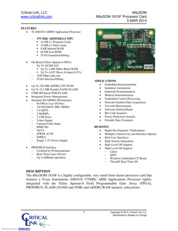
Critical Link, LLCwww.criticallink.comMitySOMMitySOM-1810F Processor Card5-MAR-2014FEATURES TI AM1810 ARM9 Application Processor- 375 MHz ARM926EJ-S MPU 16 KB L1 Program Cache 16 KB L1 Data Cache 8 KB Internal RAM 64 KB boot ROM JTAG Emulation/DebugOn-Board Xilinx Spartan-6 FPGA- Up To XC6SLX45 Up To 2,088 KBits Block RAM Up To 6,822 Slices (6 Input LUTs)- 1050 Mbps data rate- JTAG Interface/DebugAPPLICATIONS Embedded Instrumentation Industrial Automation Industrial Instrumentation Medical Instrumentation Embedded Control Processing Network Enabled Data Acquisition Test and Measurement Software Defined Radio Bar Code Scanners Power Protection Systems Portable Data TerminalsUp To 256 MB mDDR2 CPU RAMUp To 512 MB Parallel NAND FLASH8 MB SPI based NOR FLASHIntegrated Power ManagementStandard SO-DIMM-200 Interface- 96 FPGA User I/O Pins- 10/100 EMAC MII / MDIO- 2 UARTS- 2 McBSPs- 2 USB Ports- Video Output- Camera/Video Input- MMC/SD- SATA- ePWM, eCAP- EMIFA- Single 3.3V Power SupplyBENEFITS Rapid Development / Deployment Multiple Connectivity and Interface Options Rich User Interfaces High System Integration High Level OS Support High Level OS Support- Linux- QNX- Windows Embedded CE Ready- ThreadX Real Time OSPROFIBUS Interface- Certified by PI International- Real-Time Linux Drivers- Up to 6Mbaud operationDESCRIPTIONThe MitySOM-1810F is a highly configurable, very small form-factor processor card thatfeatures a Texas Instruments AM1810 375MHz ARM Applications Processor tightlyintegrated with the Xilinx Spartan-6 Field Programmable Gate Array (FPGA),PROFIBUS, FLASH (NAND and NOR) and mDDR2 RAM memory subsystems.1Downloaded from Arrow.com.Copyright 2012, Critical Link LLCSpecifications Subject to Change
Critical Link, LLCwww.criticallink.comMitySOMMitySOM-1810F Processor Card5-MAR-2014The design of the MitySOM-1810F allows end users the capability to developprograms/logic images for both the ARM processor and the FGPA. The MitySOM1810F provides a complete and flexible digital processing infrastructure necessary for themost demanding embedded applications development.The AM1810 includes an ARM926EJ-S micro-processor unit (MPU) capable of runningthe rich software applications programming interfaces (APIs) expected by modern systemdesigners. The ARM architecture supports several operating systems, including RealTime Linux, QNX and Windows XP embedded. Linux drivers are available for allinterfaces, including the PROFIBUS interface.8MB NOR Flash(SPI interface)For uBootbootloaderUp To 256MBmDDR Memory16-bit wide1.2VUp To 512MBNAND Flash16-bit wideFor root FFS1.8V2.5VPowerManagement3.3VEMIFA SD 1LCDuPPXilinxSpartan-6FPGAUp To XC6SLX45CSG324 pkg.Programmable I/OI/O Bank PowerBoot ConfigResets & RTCSATAUSB 0,1TimerseCAPeHRPWMI2C 0,1McASPSPI 0,1McBSP 0,1MMCSD 0UART 0,1,2EMAC MII/MDIOBootConfigFPGA I/OBanks can be1.8V, 2.5V, or3.3VI/O Bank PowerVPIF I/OGND(Many pins are multiplexed between peripherals)UHPI3.3 VEMAC RMIIProgrammable I/OTexas InstrumentsAM1810375-MHz ARM926EJ-S RISC MPUSO-DIMM-200 (DDR2 Connector)Figure 1 MitySOM-1810F Block DiagramFigure 1 provides a top level block diagram of the MitySOM-1810F processor card. Asshown in the figure, the primary interface to the MitySOM-1810F is through a standardSO-DIMM-200 card edge interface. The interface provides power, synchronous serialconnectivity, and up to 96 pins of configurable FPGA I/O for application definedinterfacing. Details of the SO-DIMM-200 connector interface are included in the SODIMM-200 Interface Description, below.2Downloaded from Arrow.com.Copyright 2012, Critical Link LLCSpecifications Subject to Change
Critical Link, LLCwww.criticallink.comMitySOMMitySOM-1810F Processor Card5-MAR-2014PROFIBUS InterfaceTexas Instruments Inc. (TI) has integrated PROFIBUS functionality into its AM1810Sitara ARM microprocessor (MPU). The solution utilizes one of the onboard UARTSand connects directly to the RS-485 transceiver and therefore eliminates the need of anexternal PROFIBUS ASIC or FPGA. Customers using the MitySOM-1810 in theirindustrial application can save cost and reduce design complexity as well as PCB space.Furthermore, the industrial application benefits from the low-power architecture of theSitara ARM MPU and the MitySOM-1810 platform from TI and Critical Link.The AM1810 Sitara ARM MPU PROFIBUS Slave solution has been certified byPROFIBUS International (PI).The PROFIBUS real-time frame handler (Fieldbus Data Link or FDL) is encapsulated inthe Programmable Real-Time Unit Subsystem (PRUSS), which is part of the AM1810Sitara ARM MPU on-chip peripherals. The PRUSS uses one Universal AsynchronousReceiver/Transmitter (UART) and a timer to generate PROFIBUS-compliant frames. Theindustrial application and the PROFIBUS DP-Protocol (Layer 7) are operated on theARM. The solution can be completed with an RS-485 transceiver suitable for harshenvironments, such as TI’s ISO1176T or ISO1176 placed on the base board to theMitySOM-1810F.The PROFIBUS subsystem uses the PRUs that implement real-time frame handling;PROFIBUS message transmission, frame validation and communication with the ARMprocessor. The PROFIBUS subsystem interfaces with one of the UARTs in the AM1810Sitara ARM MPU, which is designated for PROFIBUS communication at up to 6Mbauddata rate. The PRU uses interrupts to interact with the ARM where the PROFIBUS stack(Layer 7, DP Protocol) and the industrial application is run. All process data handling likecyclic, acyclic and service access point (SAP) between the PROFIBUS stack on ARMand the PRU is through the internal memory.Additional details about the AM1810 Sitara ARM MPU, available peripherals and theirfeatures are provided in the data sheet at the TI website (www.ti.com/am1810).FPGA Bank I/OThe MitySOM-1810F provides 96 lines of FPGA I/O directly to the SO-DIMM-200 cardedge interface. The 96 lines of FPGA I/O are distributed across 2 banks of the FPGA.These I/O lines and their associated logic are completely configurable within the FPGAat the end user’s discretion.With the Xilinx Spartan-6 series FPGA, up to the XC6SLX45, each of the user controlledbanks may be configured to operate on a different electrical interface standard based oninput voltage provided at the card edge connector. The banks support 3.3V, 2.5V, and1.8V standard CMOS switching level technology. In addition, the I/O lines from theFPGA have been routed as differential pairs and support higher speed LVDS standards aswell as SSTL 2.5 switching standards. Various forms of termination (pull-up/pull-down,3Downloaded from Arrow.com.Copyright 2012, Critical Link LLCSpecifications Subject to Change
Critical Link, LLCwww.criticallink.comMitySOMMitySOM-1810F Processor Card5-MAR-2014digitally controlled impedance matching) are available within the FPGA switch fabric.Refer to the Xilinx Spartan 6 user’s guide for more information.AM1810 mDDR2 Memory InterfaceThe AM1810 includes a dedicated DDR2 SDRAM memory interface. The MitySOM1810F includes up to 256 MB of mDDR2 RAM integrated with the AM1810 processor.The bus interface is capable of burst transfer rates of 532 MB / second.AM1810 SPI NOR FLASH InterfaceThe MitySOM-1810F includes 8 MB of SPI NOR FLASH. This FLASH memory isintended to store a factory provided bootloader, and typically a compressed image of aLinux kernel for the ARM core processor.EMIFA / NAND FLASH InterfaceThe Asynchronous External Memory Interface (EMIFA) interface available on theAM1810 is available on the SO-DIMM-200 connector. The EMIFA interface includes 3chip select spaces. The EMIF interface supports multiple data width transfers and buswait state configurations based on chip select space. 8, and 16 bit data word sizes may beused.Up to 512 MB of on-board NAND FLASH memory is connected to the AM1810 usingthe EMIFA bus. The FLASH memory is 8 bits wide and is connected to the third chipselect line of the EMIFA (CE1). The FLASH memory is typically used to store thefollowing types of data:-ARM Linux / Windows Embedded CE / QNX embedded root file-systemFPGA application imagesruntime ARM softwareruntime application data (non-volatile storage)AM1810 Camera and Video InterfacesThe AM1810 includes an optional video port I/O interface commonly used to drive LCDscreens as well as a camera input interface. These interfaces have been routed directly tothe SO-DIMM-200 connector.Debug InterfaceBoth the JTAG interface signals for the FPGA and the JTAG signals for the AM1810processor have been brought out to a Hirose header that is intended for use with anavailable Critical Link breakout adapter. This header can be removed for productionunits; please contact your Critical Link representative for details.This adapter is not included with individual modules but is included with each CriticalLink Development Kit that is ordered. If an adapter, Critical Link (CL) part number 80000286, is needed please contact your Critical Link representative.4Downloaded from Arrow.com.Copyright 2012, Critical Link LLCSpecifications Subject to Change
Critical Link, LLCwww.criticallink.comMitySOMMitySOM-1810F Processor Card5-MAR-2014Software and Application Development SupportUsers of the MitySOM-1810F are encouraged to develop applications using theMitySOM-1810F software development kit provided by Critical Link LLC. Thedevelopment kit includes an implementation of an OpenEmbedded board supportpackage providing an Angstrom based Linux distribution and compatible gcc compilertool-chain with debugger.To support rapid FPGA and applications development, netlist components - compatiblewith the Xilinx ISE FPGA synthesis tool – for commonly used FPGA designs and acorresponding set of Linux loadable kernel modules are included. The libraries providethe necessary functions needed to configure the MitySOM-1810F, program standaloneembedded applications, and interface with the various hardware components both on theprocessor board as well as a custom application carrier card. The libraries include severalinterface “cores” – FPGA and ARM software modules designed to interface with varioushigh performance data converter modules (ADCs, DACs, LCD and touchscreeninterfaces, etc) – as well as bootloading and FLASH programming utilities.Growth OptionsThe MitySOM-1810F has been designed to support several upgrade options. Theseoptions include various speed grades, memory configurations, and operating temperaturespecifications including commercial and industrial temperature ranges. The availableoptions are listed in the section below containing ordering information. For additionalordering information and details regarding these options, or to inquire about a particularconfiguration not listed below, please contact a Critical Link sales representative.5Downloaded from Arrow.com.Copyright 2012, Critical Link LLCSpecifications Subject to Change
Critical Link, LLCwww.criticallink.comMitySOMMitySOM-1810F Processor Card5-MAR-2014ABSOLUTE MAXIMUM RATINGSOPERATING CONDITIONSIf Military/Aerospace specified cards arerequired, please contact the Critical Link SalesOffice or unit Distributors for availability andspecifications.Ambient TemperatureRange CommercialAmbient TemperatureRange IndustrialHumidityMaximum Supply Voltage, VccStorage Temperature RangeShock, Z-AxisShock, X/Y-Axis3.5 VMIL-STD-810F-65oC to 80oC 10 g 10 g0oC to 70oC-40oC to 85oC0 to 95%Non-condensingContact CriticalLink for DetailsSO-DIMM-200 Interface DescriptionThe primary interface connector for the MitySOM-1810F is the SO-DIMM card /OI/OI/OI/OI/OI/OTable 1 SO-DIMM Pin-OutSignalPinI/O 3.3 V in2 3.3 V in4 3.3 V in6GND8GND10RESET IN#12SATA TX P14I/OSATA TX N16I/OSATA RX P18I/OSATA RX N20I/OUSB0 ID22I/OUSB1 D N24I/OUSB1 D P26I/OUSB0 VBUS28I/OUSB0 D N30I/OUSB0 D P32I/OUSB0 DRVVBUS34I/O3V RTC Battery36I/O 3.3 V in38 3.3 V in40GND42SPI1 MISO44I/OSPI1 MOSI46I/OSPI1 ENA48I/OSPI1 CLK50I/OSPI1 SCS152I/OReserved54I/OI2C0 SCL56I/OI2C0 SDA58I/O6Downloaded from Arrow.com.Signal 3.3 V in 3.3 V in 3.3 V inGNDGNDEXT BOOT#GP0 7GP0 10GP0 11GP0 15GP0 6GP0 14GP0 12GP0 5GP0 13GP0 1GP0 4GP0 3 3.3 V in 3.3 V inGNDGP0 2GP0 0GP0 8GP0 9MMCSD0 DAT7MMCSD0 DAT6MMCSD0 DAT5MMCSD0 DAT4Copyright 2012, Critical Link LLCSpecifications Subject to Change
Critical Link, SOMMitySOM-1810F Processor Card5-MAR-2014SignalUART2 TXD/I2C1 SDAUART2 RXD / I2C1 SCLGNDUART1 TXDUART1 RXDMDIO CLKMDIO DATMII RXCLKMII RXDVMII RXD0MII RXD1MII RXD2MII RXD3GNDMII CRSMII RXERB1 47 P.U17B1 47 N.U18B1 45 P.T17B1 45 N.T18B1 43 P.P17B1 43 N.P18B1 41 P.N17B1 41 N.N18GNDB1 39 P.M16B1 39 N.M18B1 37 P.L17B1 37 N.L18B1 35 P.K17B1 35 N.K18B1 33 P.J16B1 33 N.J18B1 31 P.H17B1 31 N.H18GNDB1 29 P.G16B1 29 N.G18B1 27 P.F17B1 27 N.F18B1 25 P.E16B1 25 N.E18B1 23 P.D17B1 23 N.D18B1 21 P.C17B1 21 N.C18GNDB0 19 P.B16B0 19 N.A16B0 17 P.C157Downloaded from Arrow.com.Pin60I/OI/OSignalMMCSD0 /OI/OI/OI/O*I/O*I/O*MMCSD0 DAT2GNDMMCSD0 DAT1MMCSD0 DAT0MMCSD0 CMDMMCSD0 CLKMII TXCLKMII TXD3MII TXD2MII TXD1MII TXD0MII TXENGNDMII COLFPGA SUSPENDB1 48 P.M14B1 48 N.N14B1 46 P.N15B1 46 N.N16B1 44 P.L12B1 44 N.L13B1 42 P.K12B1 42 N.K13GNDB1 40 P.L15B1 40 N.L16B1 38 P.K15B1 38 N.K16B1 36 P.J13B1 36 N.K14B1 34 P.H15B1 34 N.H16B1 32 P.H13B1 32 N.H14GNDB1 30 P.F15B1 30 N.F16B1 28 P.H12B1 28 N.G13B1 26 P.F14B1 26 N.G14B0 24 P.F13B0 24 N.E13B0 22 P.D14B0 22 N.C14GNDB0 20 P.F12*B0 20 N.E12*B0 18 P.D12*Copyright 2012, Critical Link LLCSpecifications Subject to Change
Critical Link, MMitySOM-1810F Processor Card5-MAR-2014SignalB0 17 N.A15B0 15 P.B14B0 15 N.A14B0 13 P.C13B0 13 N.A13B0 11 P.B12B0 11 N.A12GNDB0 9 P.B11B0 9 N.A11B0 7 P.C10B0 7 N.A10B0 5 P.B9B0 5 N.A9B0 3 P.B8B0 3 N.A8B0 1 P.C7B0 1 N.A7GNDVCCO 1VCCO /OI/OI/OI/OI/OI/OI/OI/OI/O-SignalB0 18 N.C12*B0 16 P.F11*B0 16 N.E11*B0 14 P.D11B0 14 N.C11B0 12 P.E7*B0 12 N.E8*GNDB0 10 P.D9B0 10 N.C9B0 8 P.D8B0 8 N.C8B0 6 P.D6B0 6 N.C6B0 4 P.B6B0 4 N.A6B0 2 P.C5B0 2 N.A5GNDVCCO 0VCCO 0* The Xilinx 6SLX45 FPGA does not bond I/O Buffers to balls E7, E8, F11,E11, D12, C12, E12, and F12 of the package used for this module. ForMitySOM-1810F configurations using this FPGA option, these edgeconnector signals should be treated as no-connects and will not function asFPGA I/O lines.The signal group description for the above pins is included in Table 2Table 2 Signal Group DescriptionSignal / Group3.3 V inEXT BOOT#I/ON/AIRESET IN#ISPI XXXXI/OMII XXXXI/ODescription3.3 volt input power referenced to GND.Bootstrap configuration pin. Pull low to configurebooting from external UART1.Manual Reset. When pulled to GND for aminimum of 1 usec, resets the DSP processor.The pins with an SPI prefix are directconnections to the AM1810 pins supporting theSPI1 interface. The SPI1 CLK, SPI1 ENA,SPI1 MISO, SPI1 MOSI pins must remainconfigured for the SPI function in order to supportinterfacing to the on-board SPI boot ROM. Fordetails please refer to the AM1810 processorspecifications.The pins with an MII prefix are directconnections to the AM1810 pins supporting the8Copyright 2012, Critical Link LLCSpecifications Subject to ChangeDownloaded from Arrow.com.
Critical Link, LLCwww.criticallink.comSignal / GroupMitySOMMitySOM-1810F Processor Card5-MAR-2014I/OMDIO XXI/OGP0 XIOSATA TX P/NOSATA RX P/NIGNDBX Y P.ZZ,BX Y N.ZZVCCO XUSB0 XXXX,USB1 XXXXN/AIOII/ODescriptionmedia independent interface (MII) function. TheMII pins provide multiplex capability and mayalternately be used as UART, GPIO, and SPIcontrol pins. For details please refer to theAM1810 processor specification.The MDIO CLK and MDIO DAT signals aredirect connects to the corresponding MDIOsignals on the AM1810 processor. These pinsmay be configured for GPIO.General Purpose / multiplexed pins. These pins aredirect connects to the corresponding GP0[X] pinson the AM1810 processor. The include supportfor the McASP, general purpose I/O, UART flowcontrol, and McBSP 1. For details please refer tothe AM1810 processor specifications.These pins are direct connects to the AM1810SATA TX differential Serial ATA controller pins.These pins are direct connects to the AM1810SATA RX differential Serial ATA controller pins.System Digital Ground.FPGA I/O pins. These pins are routed directly toFPGA pins ZZ. The “X” indicates which FPGAbank the pin is allocated. The bank is either 0 or1. The FPGA fabric supports routing pins indifferential pairs, the Y P and Y N portion of thename indicates the pair number and polarity. Thepins have been routed in pairs with phase matchedline lengths.FPGA Bank interface power input. These pinsmust be tied to the desired voltage used for theFPGA Bank 0 or 1 interface pins. Please refer tothe VCCO input pin specifications for the XilinxSpartan 6 family of devices for furtherinformation. Typical values are 3.3V and 2.5volts.The USBN prefixed pins are direct connects tothe corresponding pins on the AM1810 processor.For details please refer to the AM1810 processorspecifications.9Downloaded from Arrow.com.Copyright 2012, Critical Link LLCSpecifications Subject to Change
Critical Link, LLCwww.criticallink.comMitySOMMitySOM-1810F Processor Card5-MAR-2014DEBUG INTERFACEBelow is the pin-out for the Hirose 31 pin header (DF9-31P-1V(32)) that interfaces withan available adapter board, CL part number 80-000286, to debug the AM1810 andFPGA.Debug Interface Connector Description GNDGNDGNDGNDGNDGNDGNDGNDGNDGNDGNDGNDTable 3 OMAP-L138 Hirose ConnectorSignalPinI/OSignal2OOMAP EMU14OOMAP EMU06IOMAP TCK8OOMAP RTCK10OOMAP TDO12OMAP VCC / 3.3V14IOMAP TDI16IOMAP TRST18IOMAP TMS20GND22OFPGA VREF / VCCAUX24IFPGA TMS26IFPGA TCK28OFPGA TDO30IFPGA TDIELECTRICAL CHARACTERISTICSSymbolV33I33I33-maxFCPUFEMIFTable 4: Electrical ge supply, 3.3 volt input.3.23.33.4VoltsQuiescent Current draw, 3.3 volt inputTBSTBSmAMax current draw, positive 3.3 volt input.TBSTBSmACPU internal clock Frequency (PLL output)25375375MHzEMIF bus frequencyMust be ½ CPU100MHz1. Power utilization of the MitySOM-1810F is heavily dependant on end-user application. Majorfactors include: ARM CPU PLL configuration, DSP Utilization FPGA utilization, and externalDDR2 RAM utilization.10Downloaded from Arrow.com.TypCopyright 2012, Critical Link LLCSpecifications Subject to Change
Critical Link, LLCwww.criticallink.comMitySOMMitySOM-1810F Processor Card5-MAR-2014ORDERING INFORMATIONThe following table lists the standard module configurations. For shipping status,availability, and lead time of these or other configurations please contact your CriticalLink ble 5: Standard Model NumbersNORARM SpeedFPGANAND FlashFlash375 MHz6SLX168MB256MB375 MHz6SLX168MB256MBRAM128MB128MBOperatingTemp0oC to 70o C-40oC to 85o CMECHANICAL INTERFACEA mechanical outline of the MitySOM-1810F is illustrated in Figure 2, below.Figure 2 MitySOM-1810F Mechanical Outline11Downloaded from Arrow.com.Copyright 2012, Critical Link LLCSpecifications Subject to Change
Critical Link, LLCwww.criticallink.comMitySOMMitySOM-1810F Processor Card5-MAR-2014REVISION HISTORYDate23-FEB-201211-DEC-20125-MAR-2014Change DescriptionPreliminary Draft, Updates and ReleaseUpdate Debug Header information, added MIL-STD-810F andUp To notation for RAM and NANDUpdate MitySOM product name.12Downloaded from Arrow.com.Copyright 2012, Critical Link LLCSpecifications Subject to Change
Furthermore, the industrial apSOLFDWLRQEHQH¿WVIURPWKHORZ-power architecture of the Sitara ARM MPU and the MitySOM-1810 platform from TI and Critical Link. The AM1810 Sitara ARM MPU PROFIBUS Slave solution has been certified by PROFIBUS International (PI). The PROFIBUS real-time frame handler (Fieldbus Data Link or FDL) is encapsulated in