Transcription
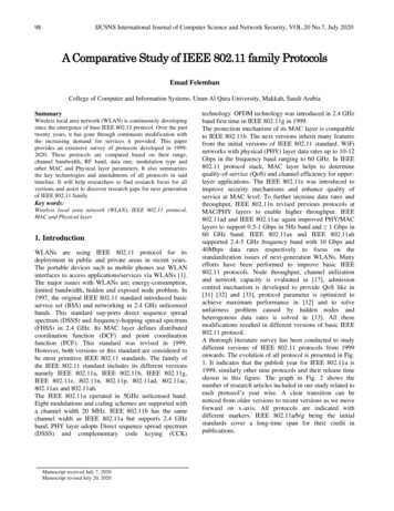
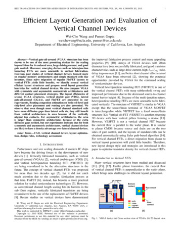
IEEE TRANSACTIONS ON COMPUTER-AIDED DESIGN OF INTEGRATED CIRCUITS AND SYSTEMS, VOL. XX, NO. Y, MONTH XX, 2015.1Efficient Layout Generation and Evaluation ofVertical Channel DevicesWei-Che Wang and Puneet Guptaweichewang@ucla.edu, puneet@ee.ucla.eduDepartment of Electrical Engineering, University of California, Los AngelesAbstract—Vertical gate-all-around (VGAA) structure has beenshown to be one of the most promising devices for the scalingbeyond 10nm for its reduced area, large driving current, and goodgate control. Moreover, emerging devices such as heterojunctiontunneling FETs are more amenable to vertical fabrication.However, past studies of vertical channel devices focused moreon regular memory architectures and simple standard cells likeinverters. Since naı̈ve migration of regular FinFET layouts tovertical FETs yields little benefits, we identify several verticalefficient layout structures and propose novel layout generationheuristics for vertical channel devices. We also compare VGAAwith symmetric and asymmetric source/drain architectures anddifferent contact placement strategies. The layout efficiencies ofseveral VGAA structures, vertical double gate (VDG), lateralgate-all-around (LGAA), and FinFET are presented in ourexperiments. Routing congestion estimation on both cell-level andchip-level after placement and routing are also presented. Weobserve that even though most vertical channel standard cellshave more diffusion gaps than lateral cells do, they still benefitfrom vertical architectures in area because of the verticallyaligned top contacts. For asymmetric architectures, the areais larger than symmetric architectures because of the extradiffusion gaps needed, but our experiments indicate that for bothsymmetric and asymmetric architectures, vertical channel devicesare likely to have a density advantage over lateral channel devices.Index Terms—CAD, vertical channel device, layout optimization, design rules, technology accessment.I. I NTRODUCTIONPerformance and size scaling demands of modern IC chipshave become the driving forces to the development of newdevices [1]. Vertically fabricated transistors, such as verticalgate-all-around (VGAA) [2], vertical double-gate (VDG) [3],and vertical heterojunction tunneling FET (VHTFET) [4]are being considered to be the alternative structures in thefuture. The concept of vertical channel FETs was proposedfor more than two decades ago [5], but it did not catchmuch attention due to the complex fabrication process atthat time. FinFET [6], instead, has become a more practicalsolution for scaled semiconductor technologies [7]. However,as conventional channel length scaling hits its barriers in thesub-10nm regime, vertically fabricated transistors are beingreconsidered to be one of the replacements of FinFET devices[8]. Recent studies on vertical devices have demonstratedW. Wang and P. Gupta are with the Electrical Engineering Department,University of California Los Angeles, Los Angeles, CA 90095 USA. email:(weichewang@ucla.edu; puneet@ee.ucla.edu).This work is supported by IMPACT center (http://impact.ee.ucla.edu).Copyright (c) 2015 IEEE. Personal use of this material is permitted.However, permission to use this material for any other purposes must beobtained from the IEEE by sending an email to pubs-permissions@ieee.org.the improved fabrication process control and many appealingproperties [9], [10]. Arrays of VGAA devices with 20nmdiameter have been successfully fabricated, and good transistorcharacteristics such as large drive current, high Ion /Iof f ratio,delay improvement [11], and better short channel effect controlof VGAA have been observed [2], showing the potentialopportunities provided by VGAA for the continued scalingof semiconductor devices.Vertical heterojunction tunneling FET (VHTFET) is one ofthe vertical channel FETs with steep subthreshold swing andimproved performance due to the decreased source-to-channeltunnel barrier height [4]. Because of the multi-junction nature,heterojunction tunneling FETs are more amenable to be fabricated vertically. The structure of VHTFET is similar to VGAAexcept that the source/drain terminal of VGAA MOSFETis interchangeable while VHTFET has a fixed source/drainstructure [12]. Vertical slit FET (VESFET) is another emerging3D device with four vertical pillars forming a device [13].However, VESFET is not a vertical channel FET becausethe current flow is parallel to the wafer plane. It is similarto planar CMOS because source and drain are on the twosides of gate control, and the layouts of standard cells can beobtained automatically using Euler path-based algorithm [14].For vertical channel FETs, a direct migration from planar tovertical layout generation will yield little benefits. Therefore,new layout design style and strategies are introduced in thispaper to optimize transistor density for vertical channel FETs.A. Introduction to Vertical FETsMany vertical structures have been studied and discussed[11], [15], [12]. Unlike planar transistors, the current flowof vertical channel FETs is perpendicular to the wafer plane,which brings new challenges to efficient layout generation.Fig. 1. VGAA device: (a) Cross section view of VGAA. (b) 2D layout view.
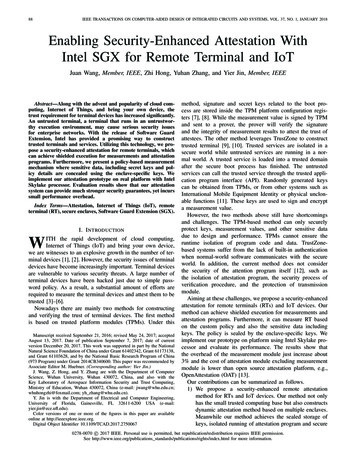
IEEE TRANSACTIONS ON COMPUTER-AIDED DESIGN OF INTEGRATED CIRCUITS AND SYSTEMS, VOL. XX, NO. Y, MONTH XX, 2015.Figure 1 shows the cross section and 2D layout view of aVGAA transistor. Two ends of the vertical pillar are doped,and the middle of the pillar is surrounded by polysilicon gate.Contacts are connected to the top, bottom, and gate of thevertical pillar. Note that the gate extension can be aligned withthe bottom and top contact plane [11] as shown in Figure 1(a),or be perpendicular to the bottom and top contact plane [12]as shown in the 2D layout in Figure 1(b). The efficient layoutgeneration proposed in this paper is applicable to both verticalstructures. However, we focus on the structure presented inFigure 1(b) because its layout resembles LGAA and FinFETmore than the layout of Figure 1(a) does. The top contactserves as either a source or a drain terminal, and so doesthe bottom contact. Interestingly, even though the source anddrain terminals are interchangeable, the device behavior differssignificantly between the two architectures. When the top tip ofvertical pillar serves as the source, the Ion is about 30% largerthan the case where substrate side serves as the source, whichcould be due to low doping on the bottom side caused by theshadowing effect [2]. However, the results in [16] show thata two-stage inverter delay is nearly 50% higher when top tipof vertical pillar serves as the source because of the increasedseries resistance and load capacitance. Therefore, the electrodeasymmetry and parasitics are important considerations forcircuit design using VGAA. In our experiments, symmetricand asymmetric VGAA structures are compared (albeit onlyfrom a layout efficiency perspective), where symmetric meansthat source and drain are interchangeable, and asymmetricmeans that the top contact can only be served as source.Besides the attractive characteristics of VGAA, anotheraspect that has impact on device performance is the crystallineorientation. Similar to FinFET, the channel of VGAA standsvertically on the wafer and can easily lie outside of thebase crystallographic plane. In fact, on a (100) wafer, thesurface orientation of VGAA is a mix of (110) and (100)because of the cylindrical channel shape. From the previouswork on surface orientation optimization of FinFET [17], thesurface orientation with the highest hole mobility and electronmobility is (110) and (100), respectively. Furthermore, sincethe PMOS enhancement on (110) is larger than the NMOSdegradation due to velocity saturation, the overall delay canbe improved by moving away from a standard (100) surfacedue to the enhancement of hole mobility.The effective device performance of vertical structurescompared to lateral structures is complex and beyond thescope of this work. Interested readers may refer to [11], [18]for some early studies. In this paper, we neglect the overallpossible benefits of vertical channel devices by comparing thearea using same effective width with lateral channel devices.Our focus is primarily to study layout efficiencies of verticalchannel devices.The VGAA fabrication process flow on 8-in bulk Si waferhas been studied and demonstrated. Figure 2 explains a common process flow [9], [10].B. Related WorkLot of research of VGAA application in memory devices hasbeen done in the past because of the potential shrinking ability2Fig. 2. Fabrication process flow of VGAA: (a) Space nitride hard maskpatterning and pillar etching. (b) As implant. (c) Oxide deposition. (d) Gateoxide growth and polysilicon gate deposition. (e) Another oxide deposition.(f) Isotropic etch and pillar top implantation.on both individual devices and multilevel memory structures[19], [15]. Studies on basic standard cells like inverter havealso been done [11]. However, since standard cells use alarge variety of layout structures, it would be difficult toevaluate the layout efficiency of a complete vertical channelstandard cell library without using a systematic framework.For planar CMOS, lateral gate-all-around (LGAA) [20], [21],[22], and FinFET, the layout generation methodologies havebeen studied [23]. Frameworks for device optimization [24]and early stage design rule evaluation were also proposed [25],[26]. However, these algorithms cannot be applied to VGAAgiven that the structure of VGAA is radically different fromplanar or lateral FETs. Previous study showing evident areareduction of a vertical channel inverter cell is given in [12].The area reduction comes from the elimination of diffusioncontacts between the adjacent polysilicon gates. Replacingthese diffusion contacts by top contacts as illustrated in Figure1(b) helps reduce area significantly.In our experiments, we extended the concept of contactspace saving and performed a fair comparison on a fullstandard cell library. In this paper, we propose a systematicframework that generates efficient VGAA standard cell layoutsand evaluates the impact of design rules as an early technologyassessment of the emerging future vertical devices.C. Our ContributionsKey contributions of this work are summarized as follows: We develop the first heuristics for effective layout generation for vertical channel devices. Layout efficiencies of several variations of VGAA, VDG,LGAA and FinFET are compared, including area andintra-cell wire length. Impact of design constraints ondesign benchmarks are also evaluated systematically. Cell-level area with intra-cell congestion estimation andchip-level area post placement and routing are bothevaluated to compare VGAA and LGAA.The rest of the paper is organized as follows. In SectionII, variations of VGAA devices, efficient/inefficient verticalstructures are described, followed by detail layout implementations such as wire length optimizations and bottomcontact placement. The cell bipartite graph representation
IEEE TRANSACTIONS ON COMPUTER-AIDED DESIGN OF INTEGRATED CIRCUITS AND SYSTEMS, VOL. XX, NO. Y, MONTH XX, 2015.and minimum chaining algorithm will be demonstrated inSection III. Section IV presents the design rules evaluationand experimental results on the proposed method. Finallyconclusions are presented in Section V.II. VGAA L AYOUT S TRUCTURESA. Variations of VGAA StructuresWe evaluated four kinds of VGAA structures to have acomprehensive understanding of the area impact of differentVGAA cell architectures and patterning technology restrictions. The four architectures of VGAA are given below: Fixed-Pitch VGAA (FVGAA): FVGAA has regular rectangular polysilicon gate shape with fixed pitch. The polysilicon gate spacing is defined as the sum of contact widthand two times of contact-poly spacing. The effectivetransistor width is the perimeter of the VGAA. Figure 3(a)shows an example of FVGAA 2D layout of an inverterwith the bottom contact serves as source and top contactsare drain terminals. The driving strength of the PMOS isequal to six VGAA pillars and three VGAA pillars forNMOS width. Contact Spacing Reduction Fixed-Pitch VGAA (RVGAA):The polysilicon gate pitch of RVGAA could be one ortwo times of the minimum polysilicon gate spacing plusa polysilicon gate width, depending on whether or not abottom contact is formed. Detailed design rules are givenin section IV. As shown in the Figure 3(b), every polysilicon gate is still located on grid, but the spacing becomesless than half if no bottom contact is placed betweentwo polysilicon gates. Therefore, RVGAA devices haveless area than FVGAA for large drive cells with multiplepolysilicon gates. Polygon-Poly VGAA (PVGAA): The architecture of PVGAA is given in Figure 3(c). Similar to [27], the shapeof the polysilicon gate depends on the number of VGAAneeded to form the cell. Array of vertical pillars aresurrounded by a large polygon polysilicon gate shape,so the area becomes much smaller than FVGAA andRVGAA because contact spacing is smaller than polysilicon gate spacing. Similar VGAA array fabrication wasdemonstrated in [2], however, lithographic patterningof the surrounding irregular polysilicon gate shape ischallenging. We include PVGAA with spacing rules sameas FVGAA in our comparison to give an idea of howmuch benefit it could have compared with FVGAA.Fig. 3. VGAA structures: (a) FVGAA. (b) RVGAA. The polysilicon gate isstill located on grid. (c) PVGAA. 3Hetero-VGAA (HVGAA): HVGAA can be considered as amixed version of RVGAA and PVGAA with different cellheights. The shape of HVGAA polysilicon gate is fixedto one or two VGAA widths plus VGAA pitch, and thecell height depends on the number of VGAAs that can beheld in a polysilicon gate shape. The number of VGAAsin each polysilicon gate shape can be viewed as arrays ofcolumns and rows “1x1”, “4x2”, or other combinationsas shown in Figure 4, where each HVGAA variationcontains eight VGAAs. The structure of standard cellswithin one library is the same so the cells can be easilyabutted and power rails can be shared. Due to the twoextra tracks left for power rails on the upper and lowerpart of the cell, the best suited HVGAA structure dependson the strengths of cells used in the design. Short HVGAA variations, such as structures shown in Figures 4(a)and 4(d), are more efficient for small driving cells. Onthe other hand, tall HVGAA variations, such as structuresshown in Figures 4(c) and 4(f), are more efficient for largedriving cells. There are dummy polysilicon gate shapesin the “4x2” structure because a diffusion space is neededfor bottom contact placement, which shows that the “4x2”structure is not an efficient structure for cells with smallnumber of VGAAs.Fig. 4. HVGAA structures: (a) 1x1 (b) 2x1 (c) 4x1 (d) 1x2 (e) 2x2 (f) 4x2B. Vertical Efficient StructuresIn this section, we will introduce vertical efficient structuresthat provide efficient layouts given the restriction of verticalchannel structure, and our VGAA default structure is FVGAA.For CMOS layouts, sharing the same active/diffusion region(what we refer to as a chain in this paper) between differenttransistors results in fewer diffusion breaks and smaller area.The definition of chain is the same as in [25], which meanspairs of P-N transistors that share a same diffusion strip. Forinstance in conventional lateral channel devices, two parallelconnected transistors and any number of series connectedtransistors can share the same diffusion region or chain. Lessnumber of chains means smaller area. Since the structure ofVGAA is radically different from lateral FETs, some CMOS
IEEE TRANSACTIONS ON COMPUTER-AIDED DESIGN OF INTEGRATED CIRCUITS AND SYSTEMS, VOL. XX, NO. Y, MONTH XX, 2015.4circuit schematics that are considered efficient in lateral FETmay not be the most efficient schematics for VGAA. Figure 5shows an example of how a 3-Parallel structure is implementedin VGAA on a single chain, while in FinFET, at least twochains are needed to realize the structure as the drain terminalsof A, B, and C are not connected. In addition, only one bottomcontact is needed for VGAA, which makes the area evensmaller.Fig. 7. 2-Stack n-m-Parallel Structure: (a) Transistor schematic. (b) VGAAcross section view.Fig. 5. 3-Parallel structure: (a) Transistor schematic. (b) FinFET. (c) VGAA.In order to find out the best structure of VGAA layout, wecategorize two types of vertical efficient layout structures. n-Parallel: The n-Parallel structure is composed of nVGAA devices with a connected source or drain terminals. The cross section view and schematic of a 3-Parallelstructure is given in Figure 6. Three VGAA devicesare shared on a same diffusion strip, where the sharedterminal can be either a source or a drain. Three gatecontacts are placed perpendicular to the bottom and topcontact plane as shown in the 2D layout Figure 1(b).Fig. 6. n-Parallel structure: (a) Transistor schematic. (b) VGAA cross sectionview.2-Stack n-m-Parallel: A 2-Stack n-m-Parallel structureconsists of two stacked n-Parallel structures, where thenumber n and m can be equal to or greater than one.Figure 7 illustrates the cross section view of a 2-Stack 33-Parallel structure. Note that for asymmetric structures,this is not a valid vertical structure because source anddrain are not interchangeable.Any circuit schematic of these two forms can be realizedusing only one vertical channel chain, and a single chain isthe preferred structure in minimizing the layout area. Theseschematic patterns for efficient layout will be identified ina systematic way and become the input to the proposedminimum chaining algorithm for vertical channel devices. C. Vertical Inefficient StructuresIn contrast to vertical efficient structures, here are twoexamples of vertical inefficient structures that can be realizedby lateral FETs in one chain but will require multiple chainsin vertical FETs. 3-Stack: A 3-Stack schematic is given in Figure 8(a). InVGAA, the minimum number of chains to realize thisstructure is two. The reason is that to form a 2-stackstructure in VGAA, the bottom diffusion must be sharedby the stacked transistors. To cut off the shared diffusion,instead of by a polysilicon gate control like FinFET, theonly way for VGAA is to introduce another chain, whichexplains why a 3-Stack structure cannot be implementedin VGAA with only one chain. Figures 8(b) and (c) showexamples of how a 3-Stack structure can be implementedin FinFET in one chain, while in VGAA the minimumnumber of chains is two.Fig. 8. 3-Stack structure: (a) Transistor schematic. (b) FinFET. Only onechain is needed. (c) VGAA. Two chains and a metal connecting segment areneeded. Stack-Parallel: A Stack-Parallel structure is similar ton-Parallel, but at least one of the paralleled structuresis a stack of transistors. Figure 9 gives an example ofa Stack-Parallel structure. Unfortunately, this structureappears in many standard cells, making most of thevertical channel structures having more chains than lateralchannel structures.D. Intra-cell Wire Length OptimizationAnother layout benefit of vertical channel is that for an nParallel chain, the bottom contact can be placed on multiple
IEEE TRANSACTIONS ON COMPUTER-AIDED DESIGN OF INTEGRATED CIRCUITS AND SYSTEMS, VOL. XX, NO. Y, MONTH XX, 2015.5tradeoffs should also be considered by adding extra constraintsto bottom contact placement, such as the maximum numberof VGAAs supported per bottom contact. For VGAAs, addingmore bottom contacts also means that more area would berequired. Figures 11(a) and (b) show two alternative layouts forfour parallel-connected devices and the tradeoff between areaand wire length. Details and comparisons of the constraintswill be presented in Section IV-D. The intra-cell wire lengthFig. 9. Stack-Parallel structure: (a) Transistor schematic. (b) FinFET. Onlyone chain needed. (c) VGAA. Two chains are needed.locations of the diffusion strip because all parallel transistorsshare diffusion region. This flexibility helps to reduce the intracell wire length of vertical channel FETs. Figure 10 shows anexample of how a wire length can be reduced by moving thebottom contacts closer to each other, where the initial locationsare on either the rightmost or the leftmost of the chain. A chainhas at most one P/N bottom contact, and each bottom contactbelongs to only one net. The total wire length estimation isobtained by summing the half parameter wire length (HPWL)of each net. Since the number and constraints of intermediaterouting layers may differ between vertical channel deviceimplementations, using HPWL provides a general estimateof the routing track usage, which is used in the congestionestimation. Note that wire length of VDD/GND is not countedin HPWL. Steps of minimizing HPWL are described below:1) For each net, identify its leftmost and rightmost ends. Ifthe two ends are on the same location horizontally, theHPWL cannot be reduced because the distance betweenPMOS part and NMOS part diffusions are assumed tobe fixed. If the two ends are not on the same locationhorizontally, proceed to step 2.2) If any of the two ends is a bottom contact, move theleftmost bottom contact to right, and move the rightmostbottom contact to left.Fig. 11. (a) One contact with higher diffusion layer parasitics. (b) Twocontacts with lower parasitics requiring larger area and extra connecting metalsegment.optimization can be adapted straightforwardly as illustrated inFigure 12 for RVGAA where a bottom contact has to be placedfor every two polysilicon gates. Instead of moving one bottomcontact on a chain, multiple contacts with fixed distances aremoved together, and a polysilicon gate is skipped whenever abottom contact is placed as described in Section II.Fig. 12. Net HPWL reduction with bottom contact constraint.Fig. 10. Net HPWL reduced by moving bottom contacts.E. Bottom Contact PlacementThough placing a bottom contact on different locations ofa chain will not affect the functionality, the high resistivity ofthe bottom diffusion layer can cause parasitics-induced performance degradation. Therefore, the performance-congestionIII. V ERTICAL C HANNEL L AYOUT G ENERATIONM ETHODOLOGYThe proposed vertical channel layout generation methodology is divided into two steps. The first step is the developmentof the bipartite graph, from which the vertical efficient layoutstructures can be easily identified. The second step is to findthe minimum number of chains by finding the minimum setof edges that cover all transistors in the bipartite graph.A. Bipartite Graph RepresentationWe first define the graph notation in a similar fashion as[23]. The triple (T, D, S) represents the three attributes of
IEEE TRANSACTIONS ON COMPUTER-AIDED DESIGN OF INTEGRATED CIRCUITS AND SYSTEMS, VOL. XX, NO. Y, MONTH XX, 2015.a transistor t, where T (t)( P or N) indicates whether t isa PMOS or NMOS, D(t) and S(t) represent the connectingnet of the drain and the source terminal respectively. A PN transistor pair P (ti , tj ), contains two transistors whereT (ti ) P and T (tj ) N . In this paper, we consider perfectpair implementation only [25], so a pair P (ti , tj ) means thatti and tj have the same gate input signal. To identify thevertical efficient layout structures, we represent the transistorschematic using a bipartite graph G (Vp Vn , E). Eachvertex in Vp or Vn corresponds to a set of PMOS or NMOStransistors that form one of the two vertical efficient layoutstructures. Once vertices are constructed, an edge is builtbetween two vertices if the two vertices contain at least oneP-N transistor pair. That is, each edge covers all the commontransistor pairs between a Vp and Vn . This is different fromthe previous work [23] because for vertical channel devices,more than two transistors in a vertex can be formed ona chain, and each edge corresponds to a chain. Once thebipartite graph is built, we apply the proposed minimum edgecovering algorithm to find out the chaining solution to the cellimplementation. The formal description of E, Vp , and Vn aregiven:Fig. 13. AOI21 schematic and bipartite graph representation: (a) Schematic.(b) Bipartite representation.TABLE IC ONNECTION TABLE OF AOI21E {Eij : t1 , t2 , ., tk {t1 , t2 , ., tk } Vp i Vn j}Vp {Vp i Vp i {tp T (tp ) P (D(tp ) i S(tp ) i)}}Vn {Vn j Vn j {tn T (tn ) N (D(tn ) j S(tn ) j)}}The description of the bipartite graph given is for symmetricstructures. The representation for asymmetric structures can beeasily obtained by first splitting each vertex representing a 2Stack n-m-Parallel into two n-Parallel vertices, and then building the edges in the same fashion. It is obvious that asymmetricstructure is very likely to have more chains than symmetricstructures because one of the two vertical efficient structuresdoes not exist anymore. In our benchmark experiments, bothsymmetric and asymmetric VGAA structures are compared.Figure 13 gives an example of the bipartite graph representation and schematic of a symmetric VGAA AOI21 standardcell. In the bipartite graph, the node Vp 1, for example, containsthree PMOS transistors that either their sources or drains areon net Vp 1 as illustrated in the schematic. Vp 1 itself representsa 2-Stack 1-2-Parallel vertical efficient structure, meaning thatPMOS transistors A, B1, and B2 can be realized on a singlechain. However, we need to consider the pairing with NMOStransistors by selecting edges in the graph. Edge E11 connectsVp 1 and Vn 1 and represents transistor pairs B1 and B2, soselecting edge E11 means that a chain is needed to realizepairs B1 and B2.B. Minimum Edge Covering AlgorithmThe goal of the algorithm is to select all P-N transistor pairswith the minimum number of edges. In the bipartite graph,each edge represents a set of P-N transistor pairs that can berealized on a chain, so a minimum edge covering algorithmis proposed to minimize the number of chains needed toimplement a cell. The notation E(P (ti , tj )) is defined as theset of edges that cover the P-N transistor pair P (ti , tj ). AP-N transistor pair P (ti , tj ) is covered if at least one edgebelonging to E(P (ti , tj )) is selected.The algorithm is described as follows: For a bipartite graph, we generate a connection tablefor all edges and pairs. Each edge is represented by acolumn, and each pair P (ti , tj ) is represented by a row.6AB1B2 E00100E02100E10101E11011E12110E20001E21011E22010If an edge covers a pair, the value of the correspondinglocation is set to one, otherwise it is set to zero. TheE(P (ti , tj )) of each pair is obtained after the connectiontable construction by finding the edges corresponding toones in the row of P (ti , tj ).Identify essential edges by observing the connectiontable. If a row contains only a single 1 or a columncontains only 1, the corresponding edge of the columnis an essential edge. Every essential edge is selectedand removed from the connection table, along with alltransistor pairs corresponding to the edge.For the remaining connection table, apply Petrickśmethod [28] by formulating the edges as Boolean variables and P-N transistor pairs as minterms. To cover aminterm P (ti , tj ), the sum of variables in E(P (ti , tj ))must be true. The logical function F (G) is defined as theproduct of all minterms, and it must be true because allminterms must be covered.F (G) is further simplified by using simple Booleansimplification technique X XY X. The product termwith the least number of edges along with essential edgesare returned by the algorithm as the minimum set of edgesto cover all P-N transistor pairs.Following the above procedure, the chaining solution of avertical channel cell is then obtained. Table I gives an exampleof the connection table of AOI21. From the table we know thatto cover P-N transistor pair of A, for example, the expression(E00 E02 E10 E12 ) must be true.Since there are no essential edges for the AOI21 cell, wedirectly apply Petrickś method to form the Boolean functions
IEEE TRANSACTIONS ON COMPUTER-AIDED DESIGN OF INTEGRATED CIRCUITS AND SYSTEMS, VOL. XX, NO. Y, MONTH XX, 2015.given below:A E00 E02 E10 E12B1 E11 E12 E21 E22B2 E10 E11 E20 E21F (G) A · B1 · B2F (G) must be true to cover all the transistor pairs A, B1,and B2. After Boolean expansion and simplification of F (G),there are eleven product terms with only two edges, whichis the minimum set of edges needed. To make F (G) true,one of these product terms is selected and set to be true, forexample, E00 E11 . Now we know that the vertical channel cellAOI21 needs two chains to be realized, and the transistor pairon the first chain E00 is A, and the transistor pairs on thesecond chain E11 are B1 and B2. The ordering of transistorswith minimum wire length is then decided by the proceduredescribed in [25], which includes solving a min-cut placementproblem and possible chain flipping. The final chaining resultof AOI21 is shown in Figure 14.The PMOS (upper) part of E11 is a 2-Parallel structure,so a bottom contact is placed as shown in Figure 5(c),while no bottom contact is placed in the NMOS (lower) partbecause it is a 2-Stack 1-1-Parallel structure similar to thestacked transistors A and B shown in Figure 8(c). Note thatfor asymmetric architecture, chain E11 will have to be splitbecause the 2-Stack 1-1-Parallel structure of the NMOS is notvalid.7structures. When the transistor is duplicated and stacked, thesizes of new transistors (A1 and A2 ) are enlarged according toits adjacent stacked transistors (B1 and B2 ) to match the delay,and the corresponding PMOS transistor is also duplicated inparallel as illustrated.Fig. 15. AOI21 improved chaining result. Transistor A is duplicated, and thenew connection forms a 2-Stack 2-2-Parallel vertical efficient structure. Onlyone chain is needed after the transformation.Nevertheles
patterning and pillar etching. (b) As implant. (c) Oxide deposition. (d) Gate oxide growth and polysilicon gate deposition. (e) Another oxide deposition. (f) Isotropic etch and pillar top implantation. on both individual devices and multilevel memory structures [19], [15]. Studies on basic standard cells like inverter have also been done [11].