Transcription
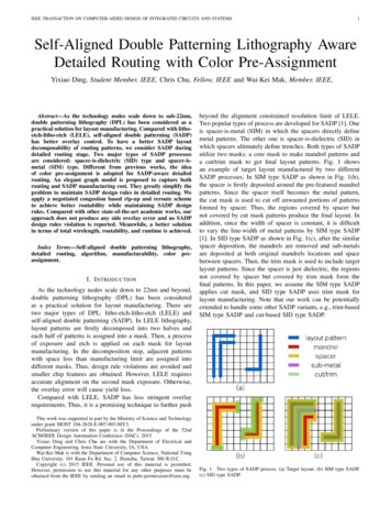
IEEE TRANSACTION ON COMPUTER-AIDED DESIGN OF INTEGRATED CIRCUITS AND SYSTEMS1Self-Aligned Double Patterning Lithography AwareDetailed Routing with Color Pre-AssignmentYixiao Ding, Student Member, IEEE, Chris Chu, Fellow, IEEE and Wai-Kei Mak, Member, IEEE,Abstract—As the technology nodes scale down to sub-22nm,double patterning lithography (DPL) has been considered as apractical solution for layout manufacturing. Compared with lithoetch-litho-etch (LELE), self-aligned double patterning (SADP)has better overlay control. To have a better SADP layoutdecomposability of routing patterns, we consider SADP duringdetailed routing stage. Two major types of SADP processesare considered: spacer-is-dielectric (SID) type and spacer-ismetal (SIM) type. Different from previous works, the ideaof color pre-assignment is adopted for SADP-aware detailedrouting. An elegant graph model is proposed to capture bothrouting and SADP manufacturing cost. They greatly simplify theproblem to maintain SADP design rules in detailed routing. Weapply a negotiated congestion based rip-up and reroute schemeto achieve better routability while maintaining SADP designrules. Compared with other state-of-the-art academic works, ourapproach does not produce any side overlay error and no SADPdesign rules violation is reported. Meanwhile, a better solutionin terms of total wirelength, routability, and runtime is achieved.Index Terms—Self-aligned double patterning lithography,detailed routing, algorithm, manufacturability, color preassignment.I. I NTRODUCTIONAs the technology nodes scale down to 22nm and beyond,double patterning lithography (DPL) has been consideredas a practical solution for layout manufacturing. There aretwo major types of DPL: litho-etch-litho-etch (LELE) andself-aligned double patterning (SADP). In LELE lithography,layout patterns are firstly decomposed into two halves andeach half of patterns is assigned into a mask. Then, a processof exposure and etch is applied on each mask for layoutmanufacturing. In the decomposition step, adjacent patternswith space less than manufacturing limit are assigned intodifferent masks. Thus, design rule violations are avoided andsmaller chip features are obtained. However, LELE requiresaccurate alignment on the second mask exposure. Otherwise,the overlay error will cause yield loss.Compared with LELE, SADP has less stringent overlayrequirements. Thus, it is a promising technique to further pushThis work was supported in part by the Ministry of Science and Technologyunder grant MOST 104-2628-E-007-003-MY3.Preliminary version of this paper is in the Proceedings of the 52ndACM/IEEE Design Automation Conference (DAC), 2015Yixiao Ding and Chris Chu are with the Department of Electrical andComputer Engineering, Iowa State University, IA, USA.Wai-Kei Mak is with the Department of Computer Science, National TsingHua University, 101 Kuan Fu Rd. Sec. 2, Hsinchu, Taiwan 300 R.O.C.Copyright (c) 2015 IEEE. Personal use of this material is permitted.However, permission to use this material for any other purposes must beobtained from the IEEE by sending an email to pubs-permissions@ieee.org.beyond the alignment constrained resolution limit of LELE.Two popular types of process are developed for SADP [1]. Oneis spacer-is-metal (SIM) in which the spacers directly definemetal patterns. The other one is spacer-is-dielectric (SID) inwhich spacers ultimately define trenches. Both types of SADPutilize two masks: a core mask to make mandrel patterns anda cut/trim mask to get final layout patterns. Fig. 1 showsan example of target layout manufactured by two differentSADP processes. In SIM type SADP as shown in Fig. 1(b),the spacer is firstly deposited around the pre-featured mandrelpatterns. Since the spacer itself becomes the metal pattern,the cut mask is used to cut off unwanted portions of patternsformed by spacer. Thus, the regions covered by spacer butnot covered by cut mask patterns produce the final layout. Inaddition, since the width of spacer is constant, it is difficultto vary the line-width of metal patterns by SIM type SADP[1]. In SID type SADP as shown in Fig. 1(c), after the similarspacer deposition, the mandrels are removed and sub-metalsare deposited at both original mandrels locations and spacebetween spacers. Then, the trim mask is used to include targetlayout patterns. Since the spacer is just dielectric, the regionsnot covered by spacer but covered by trim mask form thefinal patterns. In this paper, we assume the SIM type SADPapplies cut mask, and SID type SADP uses trim mask forlayout manufacturing. Note that our work can be potentiallyextended to handle some other SADP variants, e.g., trim-basedSIM type SADP and cut-based SID type SADP.Fig. 1. Two types of SADP process. (a) Target layout. (b) SIM type SADP.(c) SID type SADP.
IEEE TRANSACTION ON COMPUTER-AIDED DESIGN OF INTEGRATED CIRCUITS AND SYSTEMSFig. 2. SADP undecomposable layout configuration. (a) Design rule violationoccurs on cut mask in SIM process. (b) Design rule violation occurs on coremask in SID process.The LELE layout decomposition problem can be modeledas a two-coloring problem with stitch minimization [2], [3].Two patterns are assigned with different colors if they havea conflict. A pattern may be split into two parts to resolvea conflict but results in a stitch. Then layout patterns withthe same color are assigned into the same mask. Similar toLELE, SADP also requires a decomposition of the layoutinto core mask and cut/trim mask. However, SADP layoutdecomposition is more challenging since the resulting mandrelmask and cut/trim mask look significantly different fromthe target layout. A layout configuration without consideringSADP layout decomposition will probably make the layoutnot manufacturable by SADP. As shown in Fig. 2(a), afterlayout decomposition, the two adjacent cut mask patterns aretoo close and cause design rule violation. Thus, the targetlayout is not manufacturable by SIM type SADP. Similarly,a design rule violation occurs on the core mask after layoutdecomposition in Fig. 2(b). Thus, the target layout cannotbe manufactured by SID type SADP. In order to avoid theseSADP unmanufacturable patterns, it is necessary to considerSADP layout decomposition in the earlier design stage, especially in detailed routing. This will greatly improve thedecomposability of layout patterns during manufacturing time.[4] proposed an LELE-aware detailed routing algorithmwhich applied a color pre-assignment idea. Each track inthe routing grid is firstly assigned with a fixed color, thenmaze routing is performed on the grid. In this way, the maskassignment is known at the moment once a net is routed.Hence, the presence of stitches is foreknown during detailedrouting and can be easily minimized. Besides, the way that thecolors are pre-assigned enables the detailed router to generateonly decomposable layout. We extend the idea of color preassignment to our SADP-aware detailed routing. [5], [6], [7]presented the SADP layout decomposition of arbitrary 2Dpatterns in post routing stage. However, the design flexibilityis restricted in this stage and some layout patterns may benaturally undecomposable. Previous works on SADP-awaredetailed routing only focus on SID type SADP [8], [9], [10],[11], [12]. To the best of our knowledge, there is no previouswork considering SIM type SADP during detailed routingstage. [8] solved routing and layout decomposition problemssimultaneously based on the correct-by-construction approach.2However, the final routability and layout decomposabilityheavily depend on the net ordering. [9] performed routing ona grid structure where grid nodes are alternately colored bytwo colors or uncolored for SADP. However, their approachis unrealistic because it requires that every pin of each netmust fall on the same colored grid nodes, otherwise it cannotroute the net. [10] proposed an expanded routing graph model.Each point in the routing grid is split into four vertices in therouting graph, and further split into eight vertices to considerprohibited line-ends. The high complexity of routing graphwill slow down the runtime and increase memory load ofdetailed router. In addition, how to handle via in the graphmodel is not mentioned. [11] maintained a overlay constraintgraph during routing which is expensive. Meanwhile, theside overlay error cannot be avoided in the experimentalresults. [12] mainly focused on SADP-aware pin access forstandard cell instead of SADP-aware detailed routing. Colorpre-assignment is the key idea and major innovation for ourSADP-aware detailed routing. Some primitive forms of colorpre-assignment idea are proposed and applied in [13], [14],[15], [10]. [13] proposed a feature assignment method forSID type SADP layout decomposition of line-space array.They treated lines as main mandrel features alternately whileremaining lines as sub-metals. [14], [15] applied the similaridea on their SADP-aware pin access for purely unidirectionalpatterns. [10] assigned routing tracks as main mandrel tracksand sub-metal tracks alternatively before detailed routing.The contributions of this paper are summarized in thefollowings. This is the first work to systematically consider SIM typeSADP lithography during detailed routing stage. We extend the idea of color pre-assignment to both SIMand SID types SADP-aware detailed routing. The ideagreatly simplifies the problem to maintain SADP designrules in detailed routing. The novel graph models are proposed for both SIM andSID type SADP-aware detailed routing. They effectivelycapture both routing and SADP manufacturing cost. We offer the strong routing results in terms of wirelength,routability, and runtime. Furthermore, in the final routingsolution, no side overlay error is guaranteed for SADPlayout manufacturing.The rest of the paper is organized as follows. Section 2provides some preliminary information, especially the SADPdesign rules considered in the paper. Section 3 presents ourproblem formulation. Section 4 explains our proposed solutionto the problem in details. Section 5 demonstrates our experimental results. Finally, Section 6 concludes the paper.II. P RELIMINARIESAs mentioned in the previous section, it is hard to printmetal lines with mixed-width by SIM type SADP lithography.However, it is possible to manufacture patterns with mixedwidth by SID type SADP lithography. Since the focus of theSID type SADP-aware detailed routing in this paper is how toapply our key idea of color pre-assignment, we will not furtherconsider mixed-width wires. Thus, we assume that all the
IEEE TRANSACTION ON COMPUTER-AIDED DESIGN OF INTEGRATED CIRCUITS AND SYSTEMS3Fig. 3. Minimum spacing and minimum width rules.Fig. 5. Non-preferred turns caused by the spacer rounding issue. (a) Roundedspacers deposited at convex corners of a mandrel. (b) A non-preferred turnin SIM type SADP. (c) Large residue occurs at the concave corner of thesub-metal. (d) A non-preferred turn in SID type SADP.Fig. 4. SADP layout decomposition with overlay error. (a) Target layout. (b)SID type with side overlay error. (c) SID type with no side overlay error. (d)SIM type with side overlay error.metal patterns in the layout are regular with same fixed width.To successfully manufacture the layout by SADP lithography,SADP design rules should be maintained. In this section, wewill discuss the SADP design rules considered in this paperand the incurred routing constraints in detailed routing.A. Core and cut/trim mask design rulesAs mentioned before, core mask is used to make mandrelpatterns in both types of SADP. A secondary mask, a cut maskin SIM process and a trim mask in SID process, is used toform the target layout patterns. Due to the optical resolutionlimits, several design rules should be enforced in the design ofcore and cut/trim masks. In this paper, we consider minimumspacing and minimum width rules as shown in Fig 3. Theminimum spacing rule requires any two adjacent patterns onthe mask should be separated with distance at least minimumspacing value. We define Sc and Ss as the minimum spacingvalues for core and secondary masks. The minimum widthrule specifies the minimum width for every pattern on themask. Wc and Ws denote minimum width values for core andsecondary masks.B. Overlay errorThe major advantage of SADP over LELE is the betteroverlay control. However, misalignment of secondary masksometimes could still cause overlay error, which results inpattern distortions. [11] defines a side overlay error as anoverlay error occurs at a section of the side boundary of alayout pattern and tip overlay error as an overlay error occurat the line end of a layout pattern. [11] also points out tipoverlays are considered as non-critical overlays which can beignored while side overlays should be minimized to reduceyield loss. Fig. 4(b)(c) show two methods of SID type SADPlayout decomposition for target layout in Fig. 4(a). For themethod in Fig. 4(b), the pattern B will be generated with aside overlay error at upper boundary and a tip overlay errorat the right line end. However, if side boundaries of patternB are all surrounded by spacers as shown in Fig. 4(c), noside overlay error will occur in SADP layout manufacturing.Hence, an additional mandrel pattern is placed at the upperside of pattern B to provide spacer protection. We refer to theadditional mandrel pattern as an assist mandrel. To obtain zeroside overlay error in SID type SADP process, we require thatall the patterns formed from sub-metals have spacer protectionin layout decomposition. Fig. 4(d) shows the SIM type SADPlayout decomposition for the same target layout. The patternA will be generated with a side overlay error at its right sideboundary. Therefore, we require the cut mask patterns not tooverlap with side boundaries of spacers which used to formtarget layout patterns. In this way, zero side overlay error canbe achieved for SIM type SADP layout manufacturing.C. Non-preferred turns[13] observes the corner rounding of the spacer depositionaround mandrel line ends in the simulations of the mandrelcontours. [16] further observers that spacers get rounded atconvex corners of mandrels while staying sharp at concavemandrel corners. Fig. 5(a) shows the rounding issue of spacers.As a result, additional constraints need to be considered forlayout manufacturing. In SIM type SADP, if an L shape layoutpattern is formed from the rounded spacer at a convex mandrelcorner, yield loss will increase. Therefore, whenever L shapelayout patterns are formed, we prefer using spacers depositedaround concave corners of mandrels. In the case shown inFig. 5(b), pattern B is preferred over pattern A by SIM typeSADP. In SID type SADP, when an L-shape layout pattern isdefined by sub-metal, large residue will occur at its concavecorner due to the spacer rounding at the convex corner of theassist mandrel. As a result, the pattern is manufactured withdistortion by SID type SADP. In order to obtain the cleanlayout patterns, we prefer to use mandrel patterns to directlydefine L-shape layout patterns in SID type SADP lithography.
IEEE TRANSACTION ON COMPUTER-AIDED DESIGN OF INTEGRATED CIRCUITS AND SYSTEMSFig. 6. Prohibited anti-parallel line-ends. (a) A layout contains anti-parallelline-ends. (b) Minimum width rule violation occurs by SID type. (c) Minimumspacing rule violation occurs by SIM type.Fig. 5(c) shows the layout decomposition for two L-shapelayout patterns manufactured by SID type SADP. As shownin Fig. 5(d), pattern A is preferred over pattern B by SID typeSADP. [10] also identified this manufacturing challenge andcalled it sm-jogs minimization. In this paper, we refer to Lshape layout patterns manufactured by rounded spacer in SIMprocess or sub-metal in SID process as non-preferred turns.The number of non-preferred turns should be minimized indetailed routing.D. Prohibited line-endsThe prohibited line-ends refer to a particular line-endsconfiguration in the layout pattern which is prohibited duringdetailed routing due to the manufacturing challenge. [10] identified the “anti-parallel line-ends”, in which two layout patternsare on adjacent tracks and form a pair of line ends in oppositedirection. Fig. 6(a) shows a layout pattern containing an antiparallel line-ends. In the SID type SADP layout decompositionshown in Fig. 6(b), the minimum width rule is violated whentwo trim mask patterns are merged. Thus, the anti-parallel lineends should be prohibited in SID type SADP-aware detailedrouting. The anti-parallel line-ends in Fig. 6(a) should also beprohibited in SIM type SADP-aware detailed routing. This isdue to the violation of minimum spacing rule on cut mask patterns, which is shown in Fig. 6(c). Therefore, the anti-parallelline-ends should either have enough horizontal overlappinglength leno or enough horizontal separation distance dists .leno Ws and diss Ss for SID type, while leno Ss anddists Ws for SIM type.Besides, the line-ends configuration in Fig. 2(b) should beprohibited in SID type SADP-aware detailed routing due tothe minimum spacing rule violation on core mask. We referto this line-ends configuration as anti line-ends. Furthermore,the line-ends configuration in Fig. 4(d) should be prohibited inSIM type SADP-aware detailed routing due to the intolerableside overlay error during manufacturing.III. P ROBLEM FORMULATIONWe assume that there is a preferred routing direction foreach layer and the other direction perpendicular to the preferred routing direction is defined as non-preferred routing direction of the layer. We do not completely disable but stronglydiscourage routing in the non-preferred routing direction. Werefer to the above problem as the restricted detailed routingproblem. In addition, we assume all the multi-pin nets fromnetlist have been decomposed into 2-pin nets and each pinhas several candidate locations. With such assumption and4design rules mentioned in Section 2, we formulate the SADPlithography aware detailed routing problem.Given a netlist, a multi-layer routing grid, a set ofblockages, and design rules, restricted detailed routing withsimultaneous pin location determination for all the nets isperformed. The final routing patterns should be compliant todesign rules of either SIM or SID type SADP lithographyin layout manufacturing. The objective is to achieve 100%routability and to ensure zero side overlay error in SADPlayout decomposition. Besides, design rule violations, totalwirelength, the number of vias, and non-preferred turns shouldbe minimizedIV. P ROPOSED SOLUTIONA. Overall flowThe overall flow of our SADP-aware detailed routing isshown in Fig. 7. Assuming a netlist, a routing grid, a set ofblockages, and design rules are given. The routing of each netshould be along the grid lines. We firstly perform color preassignment on the routing grid, then we build a routing graphbased on our proposed graph model. After that, we performindependent routing iterations. During this phase, we route allthe nets almost independently in each iteration to minimize thenegative impact of net ordering. Several heuristics are appliedhere in order to obtain better solution in fewer number ofiterations. This phase will terminate if the congestion of thecurrent iteration is no better than the previous one. Next, wetreat the output of independent routing iterations as the initialrouting solution for the negotiated congestion based rip-up andreroute (RNR) phase. The RND iterations will continue untilthere is no congestion in the routing solution or it reachesthe pre-set maximum number of iterations. The last phase isdesign rule violation removal based RNR iterations. All theprohibited line-ends in the layout are firstly identified. Thenline end extension or cut/trim mask pattern merge is performedto resolve violations. If violations still exist, RNR is called tolegalize the routing solution. We also has a pre-set maximumnumber of RNR iterations for this phase. The iterations willstop once there is no violation or it reaches the maximumiteration count. Finally, SADP-friendly routing solution isgenerated, and congestions and design rules violations arereported if existed.B. Color pre-assignmentDifferent from LELE, SADP layout decomposition cannotbe simplified into a 2-coloring problem. Meanwhile, additionaldesign rules should be maintained and side overlay errorsneed to be avoided during layout decomposition. Those makethe consideration of SADP lithography in detailed routing aneven more complicated problem. In this situation, we adoptthe idea of color pre-assignment to simplify the problem.Before detailed routing, the routing grid is assigned colors todetermine where mandrel patterns and cut/trim mask patternscan be formed. With such restriction, the layout decompositionis known at the moment when a net is routed. In this way,SADP design rule violations and side overlay errors can beeasily avoided during detailed routing. In this subsection, we
IEEE TRANSACTION ON COMPUTER-AIDED DESIGN OF INTEGRATED CIRCUITS AND SYSTEMS5Fig. 9. SIM type and SID type SADP-aware detailed routing restrictions dueto the color pre-assignment. (a)(b) SIM type. (c)(d) SID type.Fig. 7. SADP-aware detailed routing flow.Fig. 8. Color pre-assignment for SIM and SID type SADP-aware detailedrouting. (a)(b) SIM type. (c)(d) SID type.will explain how we pre-assign colors over the routing grid.Since the color pre-assignment is performed on each layerindividually, it can be applied to a multi-layer routing grid withdifferent pitch sizes for each layer. Note that the way we docolor pre-assignment and the resulting routing restrictions forSIM and SID types SADP-aware detailed routing are different,which will be described as follows.1) SIM type: On each layer, we define a panel as thearea between two adjacent horizontal (vertical) grid lines. Wepre-assign colors to the panels alternately in both horizontaland vertical directions. Fig. 8(a) shows the colored routinggrid prepared for SIM type SADP-aware detailed routing.The colored panels specify where the mandrel patterns maybe formed. Meanwhile, mandrel pattern is required to bealigned in the middle of colored panel which is shown in Fig.8(b). Suppose the pitch size of routing tracks p is given. Toalign the metal patterns along the routing tracks, we assumewm wsp p where wm is the width of mandrel, and wspis the width of spacer. Meanwhile, wm Wc is requiredto maintain the minimum width rule. If we require that thepitch size of colored panels, which is 2p, is larger than orequal to Sc wm , the minimum spacing rule of core maskis also maintained. Since similar lithography processes areimplemented for both core and cut mask pattern fabrication,we assume Sc Ss and Wc Ws . To have better side overlaycontrol, we require wc p where wc is the width of cut mask.The cut mask patterns are aligned along the routing tracks andFig. 8(b) shows four possible locations of cut mask patternsA, B, C, and D. For the pair of patterns A and pattern B,their pitch size is 2p, thus the design rules are maintained.Under the condition of no prohibited anti-parallel line-endsin the layout pattern, the pair of B and C are separated withenough spacing, while the pair of C and D can merge. Withcolor pre-assignment and above assumption, the SADP layoutdecomposition becomes straightforward and SADP design ruleare easy to maintain.2) SID type: Different from SIM type, we pre-assign colorto routing tracks alternately in both horizontal and verticaldirections. Fig 8(c) shows the routing grid with color preassignment which prepares for SID type SADP-aware detailedrouting. The mandrel patterns are required to be formed onlyalong red tracks and should be aligned in the center, whichis shown in Fig. 8(d). Thus, the routing layout patterns alongred tracks are made directly from mandrels, while patternsalong black tracks are made from sub-metals. With similargeometric assumption for SIM type, the design rules of coremask and trim mask can be maintained. Fig. 8(d) shows fourpossible locations of trim mask patterns A, B, C, and D. Underthe condition of no prohibited anti-parallel line-ends and antiline-ends in the layout, any pair of trim mask patterns can beeither separated with enough spacing or merged.
IEEE TRANSACTION ON COMPUTER-AIDED DESIGN OF INTEGRATED CIRCUITS AND SYSTEMS3) Routing restrictions: The color pre-assignment restrictswhere mandrel patterns can be formed for both SIM and SIDtypes SADP layout decomposition. Under such restrictions,some routing patterns are not manufacturable due to thedesign rule violations, thus should be forbidden during detailedrouting. Fig. 9(a) shows three L-shape routing patterns A, B,and C, Fig. 9(b) shows their corresponding SIM type SADPlayout decomposition. A is a non-preferred turn due to thespacer rounding issue at a convex mandrel corner. B is formedfrom spacer deposited at a concave mandrel corner, thus canbe manufactured without any degradation. We refer to it as apreferred turn. The layout decomposition for C cannot avoiddesign rule violations. As shown in Fig. 9(b), both core andcut mask violate the minimum spacing rule. Hence, we referto the L-shape pattern C as a forbidden turn, and should bestrictly avoided during detailed routing. Fig. 9(c)(d) show thesame L-shape routing patterns and their corresponding SIDtype SADP layout decomposition. A is directly defined bymandrel which is free from spacing rounding issue. We referto it as a preferred turn. B is a non-preferred turn since it isformed from sub-metal. The mandrel and trim mask patternscannot even be designed for C under the restrictions of colorpre-assignment. There, the pattern C is referred as a forbiddenturn during detailed routing.From the examples above, it is observed that how a routingpattern turns at the grid point determines its manufacturability.We have a forbidden turn which cannot be manufactured, and apreferred turn and a non-preferred turn which can be manufactured without degradation and with degradation, respectively.In the next subsection, we will introduce the graph model usedin detailed routing which captures manufacturability of routingpatterns exactly.C. Graph modelIn this section, we introduce our graph model which captures both routing cost and manufacturability of routing patternin detailed routing. In addition, the graph model complexity islinear with the size of routing grid in which the constant factorcan be kept small in practice. The graph models for SIM andSID type SADP-aware detailed routing are slightly differentwhich will be described separately as follows.1) SIM type: Suppose we are given a multi-layer routing grid with color pre-assignment and a preferred routingdirection for each layer. We construct our routing graph Gby viewing each grid segment or via as a vertex. An edgeexists between two vertices if they are directly connected inthe routing grid. A cost is associated with each edge to indicatethe cost of traveling from the vertex in one end to the vertexin the other end. The construction of G is described belowby considering graph models for pin, via, and grid segmentseparately. Fig. 10 shows the graph models together with fivetypes of edges marked with different colors, including via, unitwirelength, preferred turn, non-preferred turn, and forbiddenturn. Fig. 10 (a) shows the via model for a via accessible byeight grid segments from its upper routing layer and lowerrouting layer. In the via model, an edge exists between thevertex representing the via and the vertex representing an6Fig. 10. Graph modeling for SADP-aware detailed routing. (a) via model.(b) SIM type grid segment models. (c) SID type grid segment models.accessible grid segment. In addition, if a via layer exist above(below) the via, there will be an edge connecting the vertexrepresenting the via and the vertex representing an accessiblevia from its upper (lower) via layer. The cost of the via edgeis user-defined. In the routing grid with SIM type color preassignment, four types of grid point can be identified by therelative position of the uncolored grid square. Fig. 10(b) showsthe grid segment models for the four grid segments incident toeach type of grid point. In each grid segment model, four edgetypes can be assigned with different costs to capture relativerouting and pattern manufacturability expenses. Note that thecost of the forbidden turn edges should be very high to avoida routing pattern containing a forbidden turn.2) SID type: The only difference between the graph modelsfor SIM type and SID type are the grid segment models. Inthe colored routing grid prepared for SID type SADP-awaredetailed routing, four types of grid points are identified bythe colors of two intersected tracks. For a better illustration,we use a pair to represent each type of grid points, whereits first member denotes the color of the horizontal trackand the second member denotes the color of the verticaltrack. Fig. 10(c) shows the grid segment models which arecharacterized by four types of grid points, namely hred, redi,hred, blacki, hblack, redi, and hblack, blacki. The grid segment model characterized byhred, redi contains edges withthe preferred turn type while the grid segment model characterized byhblack, blacki contains non-preferred turn type edges.For the grid segment models characterized by the other two
IEEE TRANSACTION ON COMPUTER-AIDED DESIGN OF INTEGRATED CIRCUITS AND SYSTEMSFig. 11. Invalid routes. (a)(b) A route containing a forbidden turn. (c) A routecontaining a loop structure.types, it contains edges with the forbidden turn type. Similarto the grid segment models for SIM type, different types ofedges can be assigned with different costs to capture bothrouting and manufacturing expenses.Algorithm 1 Modified Dijkstra’s algorithmInput: net with source s and sink tOutput: path for netinitialize(G, s) and priority queue P Qwhile dist(t) dovertex u PQ.dequeue()fo
IEEE TRANSACTION ON COMPUTER-AIDED DESIGN OF INTEGRATED CIRCUITS AND SYSTEMS 1 Self-Aligned Double Patterning Lithography Aware Detailed Routing with Color Pre-Assignment Yixiao Ding, Student Member, IEEE, Chris Chu, Fellow, IEEE and Wai-Kei Mak, Member, IEEE,