Transcription
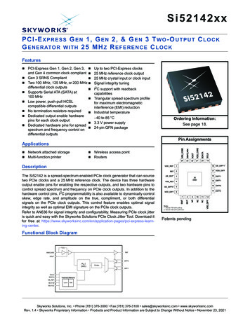
Si 52142xxPC I- E XPRESS G EN 1 , G EN 2 , & G E N 3 T WO -O U T P U T C L O C KG ENERATOR WITH 2 5 MH Z R E F E R E N C E C L O C KFeaturesDescriptionThe Si52142 is a spread-spectrum enabled PCIe clock generator that can sourcetwo PCIe clocks and a 25 MHz reference clock. The device has three hardwareoutput enable pins for enabling the respective outputs, and two hardware pins tocontrol spread spectrum and frequency on PCIe clock outputs. In addition to thehardware control pins, I2C programmability is also available to dynamically controlskew, edge rate, and amplitude on the true, compliment, or both differentialsignals on the PCIe clock outputs. This control feature enables optimal signalintegrity as well as optimal EMI signature on the PCIe clock outputs.Refer to AN636 for signal integrity and configurability. Measuring PCIe clock jitteris quick and easy with the Skyworks Solutions PCIe Clock Jitter Tool. Download itfor free at ci-express-learning-center.23SCLK24SDATAWireless access pointRouters22212019VDD REF1118 OE DIFF117 VDD DIFFREF2OE REF13VSS REF4OE DIFF015VDD DIFF616 DIFF125GND15 DIFF114 DIFF013 DIFF078910Notes:1. Internal 100 kohm pull-up.2. Internal 100 kohm pull-down.1112NC VDD DIFFNetwork attached storageMulti-function printerXOUT VDD COREPin AssignmentsApplicationsNC Ordering Information:See page 18.XIN/CLKIN NC I2C support with readbackcapabilitiesTriangular spread spectrum profilefor maximum electromagneticinterference (EMI) reductionIndustrial temperature–40 to 85 C3.3 V power supply24-pin QFN packageVSS CORE Up to two PCI-Express clocks25 MHz reference clock output25 MHz crystal input or clock inputSignal integrity tuningSS12 PCI-Express Gen 1, Gen 2, Gen 3, and Gen 4 common clock compliant Gen 3 SRNS Compliant Two 100 MHz, 125 MHz, or 200 MHz differential clock outputs Supports Serial ATA (SATA) at100 MHz Low power, push-pull HCSLcompatible differential outputsNo termination resistors required Dedicated output enable hardwarepins for each clock output Dedicated hardware pins for spread spectrum and frequency control ondifferential outputsSS02 Patents pendingFunctional Block CLKSDATAControl & MemoryOE REFOE [1:0]ControlRAMSS [1:0]Skyworks Solutions, Inc. Phone [781] 376-3000 Fax [781] 376-3100 sales@skyworksinc.com www.skyworksinc.comRev. 1.4 Skyworks Proprietary Information Products and Product Information are Subject to Change Without Notice November 23, 2021
Si 52142x x2Skyworks Solutions, Inc. Phone [781] 376-3000 Fax [781] 376-3100 sales@skyworksinc.com www.skyworksinc.comRev. 1.4 Skyworks Proprietary Information Products and Product Information are Subject to Change Without Notice November 23, 2021
Si52142xxTABLESectionOFC ONTENTSPage1. Electrical Specifications . . . . . . . . . . . . . . . . . . . . . . . . . . . . . . . . . . . . . . . . . . . . . . . . . . . 42. Functional Description . . . . . . . . . . . . . . . . . . . . . . . . . . . . . . . . . . . . . . . . . . . . . . . . . . . .72.1. Crystal Recommendations . . . . . . . . . . . . . . . . . . . . . . . . . . . . . . . . . . . . . . . . . . . . . 72.2. OE Pin Definition . . . . . . . . . . . . . . . . . . . . . . . . . . . . . . . . . . . . . . . . . . . . . . . . . . . . .82.3. OE Assertion . . . . . . . . . . . . . . . . . . . . . . . . . . . . . . . . . . . . . . . . . . . . . . . . . . . . . . . . 82.4. OE Deassertion . . . . . . . . . . . . . . . . . . . . . . . . . . . . . . . . . . . . . . . . . . . . . . . . . . . . . . 82.5. SS[1:0] Pin Definition . . . . . . . . . . . . . . . . . . . . . . . . . . . . . . . . . . . . . . . . . . . . . . . . . 83. Test and Measurement Setup . . . . . . . . . . . . . . . . . . . . . . . . . . . . . . . . . . . . . . . . . . . . . . . 94. Control Registers . . . . . . . . . . . . . . . . . . . . . . . . . . . . . . . . . . . . . . . . . . . . . . . . . . . . . . . . 114.1. I2C Interface . . . . . . . . . . . . . . . . . . . . . . . . . . . . . . . . . . . . . . . . . . . . . . . . . . . . . . . 114.2. Data Protocol . . . . . . . . . . . . . . . . . . . . . . . . . . . . . . . . . . . . . . . . . . . . . . . . . . . . . . 115. Pin Descriptions: 24-Pin QFN . . . . . . . . . . . . . . . . . . . . . . . . . . . . . . . . . . . . . . . . . . . . . . 166. Ordering Guide . . . . . . . . . . . . . . . . . . . . . . . . . . . . . . . . . . . . . . . . . . . . . . . . . . . . . . . . . . 187. Package Outline . . . . . . . . . . . . . . . . . . . . . . . . . . . . . . . . . . . . . . . . . . . . . . . . . . . . . . . . .198. Land Pattern . . . . . . . . . . . . . . . . . . . . . . . . . . . . . . . . . . . . . . . . . . . . . . . . . . . . . . . . . . . . 20Document Change List . . . . . . . . . . . . . . . . . . . . . . . . . . . . . . . . . . . . . . . . . . . . . . . . . . . . . 22Skyworks Solutions, Inc. Phone [781] 376-3000 Fax [781] 376-3100 sales@skyworksinc.com www.skyworksinc.com3Rev. 1.4 Skyworks Proprietary Information Products and Product Information are Subject to Change Without Notice November 23, 2021
Si 52142x x1. Electrical SpecificationsTable 1. DC Electrical SpecificationsParameterSymbolTest ConditionMinTypMaxUnit3.3 V Operating VoltageVDD core3.3 5%3.1353.33.465V3.3 V Input High VoltageVIHControl input pins2.0—VDD 0.3V3.3 V Input Low VoltageVILControl input pinsVSS –0.3—0.8VInput High VoltageVIHI2CSDATA, SCLK2.2——VInput Low VoltageVILI2CSDATA, SCLK——1.0VInput High Leakage CurrentIIHExcept internal pull-downresistors, 0 VIN VDD——5 AInput Low Leakage CurrentIILExcept internal pull-up resistors, 0 VIN VDD–5—— A3.3 V Output High Voltage(Single-Ended Outputs)VOHIOH –1 mA2.4——V3.3 V Output High Voltage(Single-Ended Outputs)VOLIOL 1 mA——0.4VHigh-impedance Output CurrentIOZ–10—10µAInput Pin �—40mAOutput Pin CapacitancePin InductanceDynamic Supply CurrentIDD 3.3VAll outputs enabled. Differential clocks with 5” tracesand 2 pF load.Table 2. AC Electrical SpecificationsParameterSymbolTest ConditionMinTypMaxUnitLACCMeasured at VDD/2 differential——250ppmTDCMeasured at VDD/245—55%CLKIN Rising and Falling SlewRateTR/TFMeasured between 0.2 VDD and0.8 VDD0.5—4.0V/nsCycle to Cycle JitterTCCJMeasured at VDD/2——250psCrystalLong-term AccuracyClock InputDuty CycleNotes:1. Visit www.pcisig.com for complete PCIe specifications.2. Gen 4 specifications based on the PCI-Express Base Specification 4.0 rev. 0.5.3. Download the Skyworks Solutions PCIe Clock Jitter Tool at ci-expresslearning-center.4Skyworks Solutions, Inc. Phone [781] 376-3000 Fax [781] 376-3100 sales@skyworksinc.com www.skyworksinc.comRev. 1.4 Skyworks Proprietary Information Products and Product Information are Subject to Change Without Notice November 23, 2021
Si52142xxTable 2. AC Electrical Specifications (Continued)ParameterSymbolTest ConditionMinTypMaxUnitLong Term JitterTLTJMeasured at VDD/2——350psInput High VoltageVIHXIN/CLKIN pin2—VDD 0.3VInput Low VoltageVILXIN/CLKIN pin——0.8VInput High CurrentIIHXIN/CLKIN pin, VIN VDD——35µAInput Low CurrentIILXIN/CLKIN pin, 0 VIN 0.8–35——µATDCMeasured at 0 V differential45—55%Output-Output SkewTSKEWMeasured at 0 V differential——50psCycle to Cycle JitterTCCJMeasured at 0 V differential—3550psPCIe Gen 1 Pk-Pk Jitter,Common ClockPk-PkPCIe Gen 104045psPCIe Gen 2 Phase Jitter,Common ClockRMSGEN210 kHz F 1.5 MHz01.82.0ps1.5 MHz F Nyquist Rate01.82.0psPCIe Gen 3 Phase Jitter,Common ClockRMSGEN3PLL BW 2–4 MHzCDR 10 MHz00.50.6psPCIe Gen 3 Phase Jitter,Separate Reference NoSpread, SRNSRMSGEN3 SRNSPLL BW of 2–4 or 2–5 MHz,CDR 10 MHz—0.350.42psPCIe Gen 4 Phase Jitter,Common ClockRMSGEN4PLL BW of 2–4 or 2–5 MHz,CDR 10 MHz—0.50.6psLACCMeasured at 0 V differential——100ppmRising/Falling Slew RateTR / TFMeasured differentially from 150 mV1—8V/nsVoltage HighVHIGH——1.15VVoltage LowVLOW–0.3——VCrossing Point Voltage at0.7 V SwingVOX300—550mVSpread RangeSPR—–0.5—%Modulation FrequencyFMOD3031.533kHzDIFF at 0.7 VDuty CycleLong Term AccuracyDown spreadNotes:1. Visit www.pcisig.com for complete PCIe specifications.2. Gen 4 specifications based on the PCI-Express Base Specification 4.0 rev. 0.5.3. Download the Skyworks Solutions PCIe Clock Jitter Tool at ci-expresslearning-center.Skyworks Solutions, Inc. Phone [781] 376-3000 Fax [781] 376-3100 sales@skyworksinc.com www.skyworksinc.com5Rev. 1.4 Skyworks Proprietary Information Products and Product Information are Subject to Change Without Notice November 23, 2021
Si 52142x xTable 2. AC Electrical Specifications (Continued)ParameterSymbolTest ConditionMinTypMaxUnitTDCMeasurement at 1.5 V45—55%TR / TFMeasured between 0.8 and 2.0 V1.0—4.0V/nsCycle to Cycle JitterTCCJMeasurement at 1.5 V——300psLong Term AccuracyLACCMeasured at 1.5 V——100ppmClock Stabilization fromPower-upTSTABLEMeasured from the point both VDDand clock input are valid——1.8msStopclock Set-up TimeTSS10.0——nsREF(25 MHz) at 3.3 VDuty CycleRising and Falling Edge RateEnable/Disable and Set-UpNotes:1. Visit www.pcisig.com for complete PCIe specifications.2. Gen 4 specifications based on the PCI-Express Base Specification 4.0 rev. 0.5.3. Download the Skyworks Solutions PCIe Clock Jitter Tool at ci-expresslearning-center.Table 3. Absolute Maximum ConditionsParameterSymbolTest ConditionMinTypMaxUnitVDD 3.3VFunctional——4.6VInput VoltageVINRelative to VSS–0.5—4.6VDCTemperature, StorageTSNon-functional–65—150 CTemperature, Operating AmbientTAFunctional–40—85 CTemperature, JunctionTJFunctional——150 CDissipation, Junction to CaseØJCJEDEC (JESD 51)——25 C/WDissipation, Junction to AmbientØJAJEDEC (JESD 51)——37 C/WESDHBMJEDEC (JESD 22-A114)2000——VUL-94UL (Class)Main Supply VoltageESD Protection (Human Body Model)Flammability RatingV–0Note: While using multiple power supplies, the voltage on any input or I/O pin cannot exceed the power pin during power-up. Powersupply sequencing is not required.6Skyworks Solutions, Inc. Phone [781] 376-3000 Fax [781] 376-3100 sales@skyworksinc.com www.skyworksinc.comRev. 1.4 Skyworks Proprietary Information Products and Product Information are Subject to Change Without Notice November 23, 2021
Si52142xx2. Functional Description2.1. Crystal RecommendationsIf using crystal input, the device requires a parallel resonance 25 MHz crystal.Table 4. Crystal RecommendationsFrequency(Fund)CutLoading Load Cap25 MHzATParallel12–15 pFShuntCap g(max)5 pF0.016 pF35 ppm30 ppm5 ppm2.1.1. Crystal LoadingCrystal loading is critical for ppm accuracy. In order to achieve low/zero ppm error, use the calculations below insection 2.1.2 to estimate the appropriate capacitive loading (CL).Figure 1 shows a typical crystal configuration using two trim capacitors. It is important that the trim capacitors are inseries with the crystal.Figure 1. Crystal Capacitive Clarification2.1.2. Calculating Load CapacitorsIn addition to the standard external trim capacitors, consider the trace capacitance and pin capacitance to calculatethe crystal loading correctly. The capacitance on each side is in series with the crystal. The total capacitance onboth sides is twice the specified crystal load capacitance (CL). Trim capacitors are calculated to provide equalcapacitive loading on both sides.Figure 2. Crystal Loading ExampleSkyworks Solutions, Inc. Phone [781] 376-3000 Fax [781] 376-3100 sales@skyworksinc.com www.skyworksinc.com7Rev. 1.4 Skyworks Proprietary Information Products and Product Information are Subject to Change Without Notice November 23, 2021
Si 52142x xUse the following formulas to calculate the trim capacitor values for Ce1 and Ce2.Load Capacitance (each side)Ce 2 x CL – (Cs Ci)Total Capacitance (as seen by the crystal)CLe 11( Ce1 Cs1 Ci1 1Ce2 Cs2 Ci2)CL: Crystal load capacitanceCLe: Actual loading seen by crystal using standard value trim capacitorsCe: External trim capacitorsCs: Stray capacitance (terraced)Ci : Internal capacitance (lead frame, bond wires, etc.)2.2. OE Pin DefinitionThe OE pins are active high inputs used to enable and disable the output clocks. To enable the output clock, the OEpin needs to be logic high and the I2C output enable bit needs to be logic high. There are two methods to disablethe output clocks: the OE is pulled to a logic low, or the I2C enable bit is set to a logic low. The OE pins is requiredto be driven at all time and even though it has an internally 100 k resistor.2.3. OE AssertionThe OE signals are active high input used for synchronous stopping and starting the output clocks respectively whilethe rest of the clock generator continues to function. The assertion of the OE signal by making it logic high causesstopped respective output clocks to resume normal operation. No short or stretched clock pulses are produced whenthe clock resumes. The maximum latency from the assertion to active outputs is no more than two to six output clockcycles.2.4. OE DeassertionWhen the OE pin is deasserted by making its logic low, the corresponding output clocks are stopped cleanly, andthe final output state is driven low.2.5. SS[1:0] Pin DefinitionSS[1:0] are active inputs used to select differential output frequency and enable spread of –0.5% on all DIFFoutputs as per Table 5.Table 5. SS0 and SS1 Frequency/Spread preadConfiguration00100 MHzSpread OffDefault01100 MHz–0.50%10125 MHzSpread Off11200 MHzSpread OffSkyworks Solutions, Inc. Phone [781] 376-3000 Fax [781] 376-3100 sales@skyworksinc.com www.skyworksinc.comRev. 1.4 Skyworks Proprietary Information Products and Product Information are Subject to Change Without Notice November 23, 2021
Si52142xx3. Test and Measurement SetupFigure 3 shows the test load configuration for the HCSL compatible clock outputs.M e a s u re m e n tP o in tL1O U T 50 2 pFL1 5"O U T-M e a su rem e ntP o in tL150 2 pFFigure 3. 0.7 V Differential Load ConfigurationPlease reference application note AN781 for recommendations on how to terminate the differential outputs forLVDS, LVPECL, or CML signaling levels.Figure 4. Differential Measurement for Differential Output Signals(for AC Parameters Measurement)Skyworks Solutions, Inc. Phone [781] 376-3000 Fax [781] 376-3100 sales@skyworksinc.com www.skyworksinc.com9Rev. 1.4 Skyworks Proprietary Information Products and Product Information are Subject to Change Without Notice November 23, 2021
Si 52142x xVMIN –0.30VVMIN –0.30VFigure 5. Single-ended Measurement for Differential Output Signals(for AC Parameters Measurement)L1 0.5", L2 5"SE ClocksL133 Measurement50 L2Point4 pFFigure 6. Single-ended Clocks with Single Load ConfigurationFigure 7. Single-ended Output Signal (for AC Parameter Measurement)10Skyworks Solutions, Inc. Phone [781] 376-3000 Fax [781] 376-3100 sales@skyworksinc.com www.skyworksinc.comRev. 1.4 Skyworks Proprietary Information Products and Product Information are Subject to Change Without Notice November 23, 2021
Si52142xx4. Control Registers4.1. I2C InterfaceTo enhance the flexibility and function of the clock synthesizer, an I2C interface is provided. Through the I2CInterface, various device functions are available, such as individual clock enablement. The registers associatedwith the I2C Interface initialize to their default setting at power-up. The use of this interface is optional. Clock deviceregister changes are normally made at system initialization, if any are required. Power management functions canonly be programed in program mode and not in normal operation modes.4.2. Data ProtocolThe clock driver I2C protocol accepts byte write, byte read, block write, and block read operations from thecontroller. For block write/read operation, access the bytes in sequential order from lowest to highest (mostsignificant bit first) with the ability to stop after any complete byte is transferred. For byte write and byte readoperations, the system controller can access individually indexed bytes.The block write and block read protocol is outlined in Table 6 while Table 7 outlines byte write and byte readprotocol. The slave receiver address is 11010110 (D6h).Table 6. Block Read and Block Write ProtocolBlock Write ProtocolBit18:2DescriptionStartSlave address—7 bitsBlock Read ProtocolBit18:2DescriptionStartSlave address—7 bits9Write9Write10Acknowledge from slave10Acknowledge from slave18:11Command Code—8 bits18:11Command Code—8 bits19Acknowledge from slave19Acknowledge from slaveByte Count—8 bits20Repeat start27:202836:293745:38Acknowledge from slave27:21Slave address—7 bitsData byte 1—8 bits28Read 1Acknowledge from slave29Acknowledge from slaveData byte 2—8 bits46Acknowledge from slave.Data Byte /Slave Acknowledges.Data Byte N—8 bits.Acknowledge from slave.Stop37:303846:394755:48Byte Count from slave—8 bitsAcknowledgeData byte 1 from slave—8 bitsAcknowledgeData byte 2 from slave—8 bits56Acknowledge.Data bytes from slave/Acknowledge.Data Byte N from slave–8 bits.NOT Acknowledge.StopSkyworks Solutions, Inc. Phone [781] 376-3000 Fax [781] 376-3100 sales@skyworksinc.com www.skyworksinc.com11Rev. 1.4 Skyworks Proprietary Information Products and Product Information are Subject to Change Without Notice November 23, 2021
Si 52142x xTable 7. Byte Read and Byte Write ProtocolByte Write ProtocolBit18:2DescriptionStartSlave address–7 bitsByte Read ProtocolBit18:2DescriptionStartSlave address–7 bits9Write9Write10Acknowledge from slave10Acknowledge from slave18:111927:20Command Code–8 bits18:11Command Code–8 bitsAcknowledge from slave19Acknowledge from slaveData byte–8 bits20Repeated start28Acknowledge from slave29Stop27:21Slave address–7 bits28Read29Acknowledge from slave37:30Data from slave–8 bits38NOT Acknowledge39Stop12Skyworks Solutions, Inc. Phone [781] 376-3000 Fax [781] 376-3100 sales@skyworksinc.com www.skyworksinc.comRev. 1.4 Skyworks Proprietary Information Products and Product Information are Subject to Change Without Notice November 23, 2021
Si52142xxControl Register 0. Byte 0BitD7D6D5D4D3NameTypeD2D1D0R/WR/WR/WREF OER/WR/WR/WR/WR/WReset settings 00000100BitNameFunction7:3Reserved2REF OE1:0ReservedOutput Enable for REF.0: Output disabled.1: Output enabled.Register 1. Byte peReset settings 00000000Bit7:0NameReservedFunctionSkyworks Solutions, Inc. Phone [781] 376-3000 Fax [781] 376-3100 sales@skyworksinc.com www.skyworksinc.com13Rev. 1.4 Skyworks Proprietary Information Products and Product Information are Subject to Change Without Notice November 23, 2021
Si 52142x xRegister 2. Byte 2BitD7D6NameDIFF0 OEDIFF1 set settings 11000000Bit7NameDIFF0 OE6DIFF1 OE5:0ReservedFunctionOutput Enable for DIFF0.0: Output disabled.1: Output enabled.Output Enable for DIFF1.0: Output disabled.1: Output enabled.Register 3. Byte 3BitD7D6NameTypeD5D4D3Rev Code[3:0]R/WR/WR/WVendor ID[3:0]R/WR/WR/WR/WR/WD3D2D1D0R/WR/WR/WR/WReset settings 00001000BitNameFunction7:4Rev Code[3:0]Program Revision Code.3:0Vendor ID[3:0]Vendor Identification Code.Register 4. Byte 4BitD7D6D5D4NameTypeBC[7:0]R/WR/WR/WR/WReset settings 00000110BitName7:0BC[7:0]FunctionByte Count Register.14Skyworks Solutions, Inc. Phone [781] 376-3000 Fax [781] 376-3100 sales@skyworksinc.com www.skyworksinc.comRev. 1.4 Skyworks Proprietary Information Products and Product Information are Subject to Change Without Notice November 23, 2021
Si52142xxRegister 5. Byte 5BitD7D6D5D4D3D2D1D0R/WR/WR/WR/WName DIFF Amp Sel DIFF Amp Cntl[2] DIFF Amp Cntl[1] DIFF Amp Cntl[0]TypeR/WR/WR/WR/WReset settings 11011000BitName7DIFF Amp Sel6DIFF Amp Cntl[2]5DIFF Amp Cntl[1]4DIFF Amp Cntl[0]3:0ReservedFunctionAmplitude Control for DIFF Differential Outputs.0: Differential outputs with Default amplitude.1: Differential outputs amplitude is set by Byte 5[6:4].DIFF Differential Outputs Amplitude Adjustment.000: 300 mV 001: 400 mV 010: 500 mV 011: 600 mV100: 700 mV 101: 800 mV 110: 900 mV 111: 1000 mVSkyworks Solutions, Inc. Phone [781] 376-3000 Fax [781] 376-3100 sales@skyworksinc.com www.skyworksinc.com15Rev. 1.4 Skyworks Proprietary Information Products and Product Information are Subject to Change Without Notice November 23, 2021
Si 52142x xVSS COREXIN/CLKINXOUTVDD CORESDATASCLK5. Pin Descriptions: 24-Pin QFN242322212019VDD REF1118 OE DIFF1REF217 VDD DIFFOE REF13VSS REF4OE DIFF015VDD DIFF616 DIFF125GND15 DIFF114 DIFF0789101112SS02SS12NCNCNCVDD DIFF13 DIFF0Notes:1. Internal 100 kohm pull-up.2. Internal 100 kohm pull-down.Table 8. Si52142 24-Pin QFN DescriptionsPin #NameTypeDescription1VDD REF2REF3OE REFI,PU4VSS REFGND Ground.5OE DIFF0I,PU6VDD DIFFPWR 3.3 V power supply.7SS08SS19NCNCNo Connect.10NCNCNo connect.PWR 3.3 V power supply.O, SE 3.3 V, 25 MHz crystal reference clock output.Active high input pin to enable or disable REF clock (internal 100 k pull-up).Active high input pin to enable or disable DIFF0 clock (internal 100 k pull-up).I, PD 3.3 V tolerant latch-input for enabling Frequency/ Spread selection onDIFF0 and DIFF1 outputs. Refer to Table 1 on page 4 for SS[1:0] speciI, PD fications (internal 100 k pull-down).16Skyworks Solutions, Inc. Phone [781] 376-3000 Fax [781] 376-3100 sales@skyworksinc.com www.skyworksinc.comRev. 1.4 Skyworks Proprietary Information Products and Product Information are Subject to Change Without Notice November 23, 2021
Si52142xxTable 8. Si52142 24-Pin QFN Descriptions (Continued)Pin #NameTypeDescription11NCNC12VDD DIFF13DIFF0O, DIF 0.7 V, 100 MHz differential clock output.14DIFF0O, DIF 0.7 V, 100 MHz differential clock output.15DIFF1O, DIF 0.7 V, 100 MHz differential clock output.16DIFF1O, DIF 0.7 V, 100 MHz differential clock output.17VDD DIFFPWR 3.3 V power supply.18OE DIFF1I,PU19SCLKI20SDATAI/O21VDD CORE22XOUTO25.00 MHz Crystal output, Float XOUT if using only CLKIN (Clock input).23XIN/CLKINI25.00 MHz Crystal input or 3.3 V, 25 MHz Clock Input.24VSS CORE25GNDNo connect.PWR 3.3 V power supply.Active high input pin to enable or disable DIFF1 clock (internal 100 k pull-up).I2C SCLOCK.I2C SDATA.PWR 3.3 V power supply.GND Ground.GND Ground for bottom pad of the IC.Skyworks Solutions, Inc. Phone [781] 376-3000 Fax [781] 376-3100 sales@skyworksinc.com www.skyworksinc.com17Rev. 1.4 Skyworks Proprietary Information Products and Product Information are Subject to Change Without Notice November 23, 2021
Si 52142x x6. Ordering GuidePart NumberPackage TypeTemperatureSi52142-A01AGM24-pin QFNIndustrial, –40 to 85 CSi52142-A01AGMR24-pin QFN—Tape and ReelIndustrial, –40 to 85 CLead-free18Skyworks Solutions, Inc. Phone [781] 376-3000 Fax [781] 376-3100 sales@skyworksinc.com www.skyworksinc.comRev. 1.4 Skyworks Proprietary Information Products and Product Information are Subject to Change Without Notice November 23, 2021
Si52142xx7. Package OutlineFigure 8 illustrates the package details for the Si52142. Table 9 lists the values for the dimensions shown in theillustration.Figure 8. 24-Pin Quad Flat No Lead (QFN) PackageTable 9. Package Diagram sMinNomMax0.700.000.200.750.0250.254.00 BSC2.700.50 BSC4.00 02.802.800.50Notes:1. All dimensions shown are in millimeters (mm) unless otherwisenoted.2. Dimensioning and Tolerancing per ANSI Y14.5M-1994.3. This drawing conforms to JEDEC outline MO-220, variation VGGD-8.4. Recommended card reflow profile is per the JEDEC/IPC J-STD-020specification for Small Body Components.Skyworks Solutions, Inc. Phone [781] 376-3000 Fax [781] 376-3100 sales@skyworksinc.com www.skyworksinc.com19Rev. 1.4 Skyworks Proprietary Information Products and Product Information are Subject to Change Without Notice November 23, 2021
Si 52142x x8. Land PatternFigure 9. QFN Land PatternTable 10. Land Pattern DimensionsDimensionUnit mmC14.0C24.0E0.50 BSCX10.30X22.70Y10.8020Skyworks Solutions, Inc. Phone [781] 376-3000 Fax [781] 376-3100 sales@skyworksinc.com www.skyworksinc.comRev. 1.4 Skyworks Proprietary Information Products and Product Information are Subject to Change Without Notice November 23, 2021
Si52142xxTable 10. Land Pattern Dimensions (Continued)Y22.70Notes:General1. All dimensions shown are in millimeters (mm) unless otherwise noted.2. This land pattern design is based on the IPC-7351 guidelines.Solder Mask Design3. All metal pads are to be non-solder mask defined (NSMD). Clearance between the solder mask and the metal pad is tobe 60 m minimum, all the way around the pad.Stencil Design4. A stainless steel, laser-cut and electro-polished stencil with trapezoidal walls should be used to assure good solderpaste release.5. The stencil thickness should be 0.125 mm (5 mils).6. The ratio of stencil aperture to land pad size should be 1:1 for all perimeter7. pads.8. A 2x2 array of 1.10 mm x 1.10 mm openings on 1.30mm pitch should be used for the center ground pad.Card Assembly9. A No-Clean, Type-3 solder paste is recommended.10. The recommended card reflow profile is per the JEDEC/IPC J-STD-020 specification for Small Body Components.Skyworks Solutions, Inc. Phone [781] 376-3000 Fax [781] 376-3100 sales@skyworksinc.com www.skyworksinc.com21Rev. 1.4 Skyworks Proprietary Information Products and Product Information are Subject to Change Without Notice November 23, 2021
Si 52142x xDOCUMENT CHANGE LISTRevision 0.1 to Revision 1.0 Updated Features on page 1.Updated Description on page 1.Updated Table 1 on page 4.Updated Table 2 on page 5.Updated Section 2.1 on page 7.Updated Section 2.1.1 on page 7.Updated Section 4.1 on page 11.Updated Section 4.2 on page 11.Updated Pin Descriptions on page 16.Revision 1.0 to Revision 1.1 Removed Moisture Sensitivity Level specificationfrom Table 3.Revision 1.1 to Revision 1.2 Updated Table 2.Updated Section 3.Revision 1.2 to Revision 1.3 Updated Features on page 1.Updated Description on page 1.Updated Table 2, “AC Electrical Specifications,” onpage 4.Revision 1.3 to Revision 1.4 Added test condition for Tstable in Table 2.22Skyworks Solutions, Inc. Phone [781] 376-3000 Fax [781] 376-3100 sales@skyworksinc.com www.skyworksinc.comRev. 1.4 Skyworks Proprietary Information Products and Product Information are Subject to Change Without Notice November 23, 2021
ClockBuilder ProCustomize Skyworks clock generators,jitter attenuators and networksynchronizers with a single tool. WithCBPro you can control evaluationboards, access documentation, requesta custom part number, export forin-system programming and ySupport & ksinc.com/supportCopyright 2021 Skyworks Solutions, Inc. All Rights Reserved.Information in this document is provided in connection with Skyworks Solutions, Inc. (“Skyworks”) products or services. These materials, including theinformation contained herein, are provided by Skyworks as a service to its customers and may be used for informational purposes only by the customer.Skyworks assumes no responsibility for errors or omissions in these materials or the information contained herein. Skyworks may change its documentation,products, services, specifications or product descriptions at any time, without notice. Skyworks makes no commitment to update the materials orinformation and shall have no responsibility whatsoever for conflicts, incompatibilities, or other difficulties arising from any future changes.No license, whether express, implied, by estoppel or otherwise, is granted to any intellectual property rights by this document. Skyworks assumes no liabilityfor any materials, products or information provided hereunder, including the sale, distribution, reproduction or use of Skyworks products, information ormaterials, except as may be provided in Skyworks’ Terms and Conditions of Sale.THE MATERIALS, PRODUCTS AND INFORMATION ARE PROVIDED “AS IS” WITHOUT WARRANTY OF ANY KIND, WHETHER EXPRESS, IMPLIED, STATUTORY, OROTHERWISE, INCLUDING FITNESS FOR A PARTICULAR PURPOSE OR USE, MERCHANTABILITY, PERFORMANCE, QUALITY OR NON-INFRINGEMENT OF ANYINTELLECTUAL PROPERTY RIGHT; ALL SUCH WARRANTIES ARE HEREBY EXPRESSLY DISCLAIMED. SKYWORKS DOES NOT WARRANT THE ACCURACY ORCOMPLETENESS OF THE INFORMATION, TEXT, GRAPHICS OR OTHER ITEMS CONTAINED WITHIN THESE MATERIALS. SKYWORKS SHALL NOT BE LIABLE FORANY DAMAGES, INCLUDING BUT NOT LIMITED TO ANY SPECIAL, INDIRECT, INCIDENTAL, STATUTORY, OR CONSEQUENTIAL DAMAGES, INCLUDING WITHOUTLIMITATION, LOST REVENUES OR LOST PROFITS THAT MAY RESULT FROM THE USE OF THE MATERIALS OR INFORMATION, WHETHER OR NOT THE RECIPIENTOF MATERIALS HAS BEEN ADVISED OF THE POSSIBILITY OF SUCH DAMAGE.Skyworks products are not intended for use in medical, lifesaving or life-sustaining applications, or other equipment in which the failure of the Skyworksproducts could lead to personal injury, death, physical or environmental damage. Skyworks customers using or selling Skyworks products for use in suchapplications do so at their own risk and agree to fully indemnify Skyworks for any damages resulting from such improper use or sale.Customers are responsible for their products and applications using Skyworks products, which may deviate from published specifications as a result ofdesign defects, errors, or operation of products outside of published parameters or design specifications. Customers should
Si52142xx 2 Skyworks Solutions, Inc. Phone [781] 376-3000 Fax [781] 376-3100 sales@skyworksinc.com www.skyworksinc.com Rev. 1.4 Skyworks Proprietary Information Products and Product Information are Subject to Change Without Notice November 23, 2021


![PCI Compliant - but are we secure -- FOR PRINTING IN GRAYSCALE [Read-Only]](/img/14/303-pci-3.jpg)