Transcription
Freescale Semiconductor, Inc.Order Number: MPC107TS/DRev. 0, 9/1999Semiconductor Products SectorFreescale Semiconductor, Inc. Advance InformationMPC107 PCI Bridge/Memory ControllerTechnical SummaryThis document provides an overview of the MPC107 PCI bridge/memory controller (PCIB/MC) for high-performance embedded systems. The MPC107 is a cost-effective, generalpurpose PCI bridge/memory controller for applications using PCI in networkinginfrastructure, telecommunications, and other embedded markets. It can be used inapplications such as network routers and switches, mass storage subsystems, networkappliances, and print and imaging systems.For errata or revisions to this document, refer to the website at http://www.motorola.com/powerpc.1.1 MPC107 PCI Bridge/Memory Controller FeaturesThe MPC107 provides an integrated high-bandwidth, high-performance interface betweenup to two 60x processors, the PCI bus, and main memory. This section summarizes thefeatures of the MPC107. Major features of the MPC107 are as follows: Memory interface— 64-/32-bit 100-MHz bus— Programmable timing supporting either FPM DRAM, EDO DRAM or SDRAM— High-bandwidth bus (32-/64-bit data bus) to DRAMThis document contains information on a new product under development by Motorola.Motorola reserves the right to change or discontinue this product without notice. Motorola, Inc., 1999. All rights reserved.For More Information On This Product,Go to: www.freescale.com
Freescale Semiconductor, Inc.Freescale Semiconductor, Inc.MPC107 PCI Bridge/Memory Controller Features — Supports one to eight banks of 4-, 16-, 64-, or 128-Mbit memory devices, and upto four banks of 256-Mbit SDRAM devices— Supports 1-Mbyte to 1-Gbyte DRAM memory— 144 Mbytes of ROM space— 8-, 32-, or 64-bit ROM— Write buffering for PCI and processor accesses— Supports normal parity, read-modify-write (RMW), or ECC— Data-path buffering between memory interface and processor— Low-voltage TTL logic (LVTTL) interfaces— Port X: 8-, 32-, or 64-bit general-purpose I/O port using ROM controllerinterface with programmable address strobe timing32-bit PCI interface operating up to 66 MHz — PCI 2.1-compliant— PCI 5.0-V tolerance— Support for PCI locked accesses to memory— Support for accesses to PCI memory, I/O, and configuration spaces— Selectable big- or little-endian operation— Store gathering of processor-to-PCI write and PCI-to-memory write accesses— Memory prefetching of PCI read accesses— Selectable hardware-enforced coherency— PCI bus arbitration unit (five request/grant pairs)— PCI agent mode capability— Address translation unit— Some internal configuration registers accessible from PCITwo-channel integrated DMA controller (writes to ROM/Port X not supported)———————2Supports direct mode or chaining mode (automatic linking of DMA transfers)Supports scatter gathering—read or write discontinuous memoryInterrupt on completed segment, chain, and errorLocal-to-local memoryPCI-to-PCI memoryPCI-to-local memoryPCI memory-to-local memoryMPC107 PCI Bridge/Memory Controller Technical SummaryFor More Information On This Product,Go to: www.freescale.com
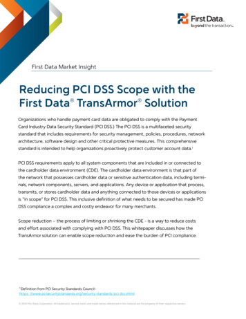
Freescale Semiconductor, Inc.MPC107 PCI/MC Applications Message unitFreescale Semiconductor, Inc.— Two doorbell registers— An extended doorbell register mechanism that facilitates interprocessorcommunication through interrupts in a dual-local-processor system— Two inbound and two outbound messaging registers— I2O message controller I2C controller with full master/slave support (except broadcast all) Embedded programmable interrupt controller (EPIC) — Five hardware interrupts (IRQs) or 16 serial interrupts— Four programmable timersIntegrated PCI bus, CPU, and SDRAM clock generation Programmable PCI bus, 60x, and memory interface output drivers Dynamic power management—Supports 60x nap, doze, sleep, and suspend modes Programmable input and output signals with watchpoint capability Built-in PCI bus performance monitor facilityDebug features — Error injection/capture on data path— IEEE 1149.1 (JTAG)/test interfaceProcessor interface————————Supports up to two PowerPC microprocessors with 60x bus interfaceSupports various operating frequencies and bus divider ratios32-bit address bus, 64/32-bit data bus supported at 100 MHzSupports full memory coherencySupports optional local bus slaveDecoupled address and data buses for pipelining of 60x accessesStore gathering on 60x-to-PCI writesConcurrent transactions on 60x and PCI buses supported1.2 MPC107 PCI/MC ApplicationsThe MPC107 can be used in either a system host configuration or as a peripheral device.For system applications where cost, space, and power consumption are critical parameters,yet performance cannot be sacrificed, the MPC107 provides a complete solution. TheMPC107 is shown in Figure 1-1 as a host bridge.MPC107 PCI Bridge/Memory Controller Technical SummaryFor More Information On This Product,Go to: www.freescale.com3
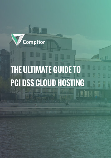
Freescale Semiconductor, Inc.MPC107 PCI/MC ApplicationsPowerPCMicroprocessorLocal Memory:DRAM, EDO,SDRAMROM /Port XMPC107DMAMU(I2O) PeripheralLogicI2CEPICDataCTRLup to 66 MHzFreescale Semiconductor, Inc.PCI BusPeripheral Peripheral Peripheral PCI to PCIBridge123PCI BusFigure 1-1. System Using MPC107 as a Host BridgeWith the embedded enhancements provided in the MPC107, it is possible to use it indistributed I/O processor applications as shown in Figure 1-2.Host ProcessorHost BridgeHost MemoryPCI Busup to 66 MHzPeripheral3Peripheral1System I/OControllerPCI to PCIBridgePCI BusPeriph. 2MPC107DMAMU(I2O) aROM /Port XLocal Memory:DRAM, EDO,SDRAMFigure 1-2. Embedded System Using the MPC107 as a Bridge to aDistributed I/O Processor4MPC107 PCI Bridge/Memory Controller Technical SummaryFor More Information On This Product,Go to: www.freescale.com
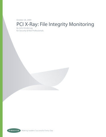
Freescale Semiconductor, Inc.MPC107 PCI/MC ApplicationsThe MPC107 can also be used with a peripheral processing device as shown in Figure 1-3.In this case, the PCI-to-PCI bridge shown Figure 1-3 could be of the PCI type 0 variety. TheMPC107 would not be part of the system configuration map. This configuration is useful inapplications such as RAID controllers or multi-port network controllers where the I/Odevices shown are SCSI controllers or Ethernet controllers, respectively.Host ProcessorFreescale Semiconductor, Inc.Host BridgeHost MemoryPCI BusPeripheral1Peripheral2PCI-to-PCIBridgeLocal PCI BusMPC107DMAMU(I2O) PeripheralLogicI2CEPICI/O Device I/O DevicePeripheral3System I/OControllerup to 66 MHzCTRLDataROM /Port XLocal Memory:DRAM, EDO,SDRAMPowerPCMicroprocessorFigure 1-3. Embedded System Using MPC107 with a Peripheral ProcessorThe processor bus interface (60x) of the MPC107 contains all of the necessary arbitrationand control logic to communicate with up to two PowerPC microprocessors in a symmetricmultiprocessing environment. In addition, the MPC107 also has a side-band mode to allowan alternate bus slave to capture address tenures. This application is show in Figure 1-4.MPC107 PCI Bridge/Memory Controller Technical SummaryFor More Information On This Product,Go to: www.freescale.com5
Freescale Semiconductor, Inc.MPC107 Major Functional x BusLocal BusFreescale Semiconductor, Inc.SlaveMPC107Local Memory:DRAM, EDO,SDRAMROM /Port XDMAMU(I2O) PeripheralLogicI2CEPICDataCTRLPCI BusFigure 1-4. Multiprocessor System Using the MPC107 and a Local Bus Slave1.3 MPC107 Major Functional BlocksThe MPC107 integrates a PCI bridge, memory controller, DMA controller, EPIC interruptcontroller/timers, a message unit with an Intelligent Input/Output (I2O) message controller,and an Inter-Integrated Circuit (I2C) controller. The integration reduces the overallpackaging requirements and the number of discrete devices required for an embeddedsystem.Figure 1-5 shows the major functional units within the MPC107. Note that this is aconceptual block diagram intended to show the basic features rather than an attempt toshow how these features are physically implemented.6MPC107 PCI Bridge/Memory Controller Technical SummaryFor More Information On This Product,Go to: www.freescale.com
Freescale Semiconductor, Inc.MPC107 Major Functional BlocksAdditional features: Programmable I/O with Watchpoint JTAG/COP Interface Power ManagementMPC10760x Bus Interface (64- or 32-Bit Data Bus)Peripheral Logic BlockMessageUnit(with I2O)Freescale Semiconductor, Inc.DMAControllerAddress(32-Bit)Data (64-Bit)Data PathECC ControllerData Bus(64- or 32-bit)with 8-bit Parityor ECCMemoryControllerMemory/ROM/Port X stersI2C5 IRQs/16 SerialInterruptsSDRAM SYNC INI2CControllerEPICInterruptController/TimersPCI BusInterface UnitAddressTranslator32-BitPCI InterfacePCIArbiterFiveRequest/GrantPairsDLLSDRAM ClocksCPU ClocksPLLPCI SYNC INFanoutBuffersPCI BusClocksOSC INFigure 1-5. MPC107 Block Diagram1.3.1 60x Processor InterfaceThe MPC107 supports a programmable interface to a variety of PowerPC microprocessorsoperating at select bus speeds. The 60x address bus is 32 bits wide and the data bus isconfigurable to be 64 or 32 bits wide. The 60x processor interface of the MPC107 uses asubset of the 60x bus protocol, supporting single-beat and burst data transfers. The addressand data buses are decoupled to support pipelined transactions.In this document, the term ‘60x’ is used to denote a 32-bit microprocessor from thePowerPC architecture family that conforms to the bus interface of the MPC603e, MPC740,MPC750, or MPC7400 microprocessors. 60x processors implement the PowerPCarchitecture as it is specified for 32-bit addressing, which provides 32-bit effective (logical)addresses, integer data types of 8, 16, and 32 bits, and floating-point data types of 32 and64 bits (single-precision and double-precision).Two signals on the MPC107, local bus slave claim (LBCLAIM) and data bus grant localbus slave (DBGLB), are provided for an optional local bus slave. However, the local busslave must be capable of generating the transfer acknowledge (TA) signal to interact withthe 60x processor(s).MPC107 PCI Bridge/Memory Controller Technical SummaryFor More Information On This Product,Go to: www.freescale.com7
Freescale Semiconductor, Inc.MPC107 Major Functional BlocksDepending on the system implementation, the processor bus may operate at the PCI busclock rate, or at a multiple of the PCI bus clock rate (determined at reset). The 60x processorbus is synchronous, with all timing relative to the rising edge of the 60x bus clock.When two 60x processors are used, the two sets of bus request, bus grant, and data bus grantsignals allow for arbitration between the 60x processors. The 60x processors share all 60xinterface signals of the MPC107, except the bus arbitration signals.Freescale Semiconductor, Inc.1.3.2 Memory System InterfaceThe MPC107 memory interface controls processor and PCI interactions to main memory.It supports a variety of DRAM, and flash or ROM configurations as main memory. TheMPC107 supports fast page mode (FPM), extended data out (EDO) and synchronousDRAM (SDRAM). The maximum supported memory size is 1 Gbyte of DRAM orSDRAM and 144 Mbytes of ROM/flash. SDRAM must comply with the JEDEC SDRAMspecification.The MPC107 implements Port X, a memory bus interface that facilitates the connection ofgeneral-purpose I/O devices. The Port X functionality allows the designer to connectexternal registers, communication devices, and other such devices directly to the MPC107.Some devices may require a small amount of external logic to properly generate addressstrobes, chip selects, and other signals.The MPC107 is designed to control a 32-bit or 64-bit data path to main memory DRAM orSDRAM. For a 32-bit data path, the MPC107 can be configured to check and generate byteparity using four parity bits. For a 64-bit data path, the MPC107 can be configured tosupport parity or ECC checking and generation with eight parity/syndrome bits checkedand generated. Note that the data bus width (32- or 64-bit) chosen at reset for the 60x businterface is also used for the memory interface.The MPC107 supports DRAM bank sizes from 1 to 128 Mbytes, SDRAM bank sizes of 1to 256 Mbytes, and provides bank start address and end address configuration registers.Note that the MPC107 does not support mixed DRAM/SDRAM configurations. TheMPC107 can be configured so that appropriate row and column address multiplexingoccurs according to the accessed memory bank. Addresses are provided to DRAM andSDRAM through a 13-bit interface for DRAM and a 15-bit interface for SDRAM.The memory bus width is configured at reset as 32- or 64-bits wide, depending on thesetting of the MDL0 reset configuration signal. Four chip selects, one write enable, oneoutput enable, and up to 21 address signals are provided for ROM/flash systems.1.3.3 Peripheral Component Interconnect (PCI) InterfaceThe PCI interface for the MPC107 is compliant with the Peripheral ComponentInterconnect Specification Revision 2.1. The PCI interface provides mode-selectable, bigto little-endian conversion. The MPC107 provides an interface to the PCI bus running atspeeds up to 66 MHz.8MPC107 PCI Bridge/Memory Controller Technical SummaryFor More Information On This Product,Go to: www.freescale.com
Freescale Semiconductor, Inc.MPC107 Major Functional BlocksThe MPC107’s PCI interface can be configured as host or agent. In host mode, the interfaceacts as the main memory controller for the system and responds to all host memorytransactions.In agent mode, the MPC107 can be configured to respond to a programmed window of PCImemory space. A variety of initialization modes are provided to boot the device.1.3.3.1 PCI Bus Arbitration UnitFreescale Semiconductor, Inc.The MPC107 contains a PCI bus arbitration unit, which eliminates the need for an externalunit, thus lowering system complexity and cost. It has the following features: Five external arbitration signal pairs. The MPC107 is the sixth member of thearbitration pool. The bus arbitration unit allows fairness as well as a priority mechanism. A two-level round-robin scheme is used in which each device can be programmedwithin a pool of a high- or low-priority arbitration. One member of the low-prioritypool is promoted to the high-priority pool. As soon as it is granted the bus, it returnsto the low-priority pool. The unit can be disabled to allow a remote arbitration unit to be used.1.3.3.2 Address Maps and TranslationThe MPC107’s processor bus interface supports memory-mapped accesses. The addressspace is divided between memory and PCI according to one of two allowable addressmaps—map A and map B. Note that the support of map A is provided for backwardcompatibility only. It is strongly recommended that new designs use map B because map Amay not be supported in future devices.An inbound and outbound PCI address translation mechanism is provided to support theuse of the MPC107 in agent mode. Note that address translation is supported only for agentmode; it is not supported when the MPC107 is operating in host mode. Also note that sinceagent mode is supported only for address map B, address translation is supported only foraddress map B.When the MPC107 is configured to be a PCI agent, the amount of local memory visible tothe system is programmable. In addition, it may be necessary to map the local memory toa different system memory address space. The address translation unit handles the mappingof both inbound and outbound transactions for these cases.1.3.3.3 Byte OrderingThe MPC107 allows the processor to run in either big- or little-endian mode (except for theinitial boot code which must run in big-endian mode).MPC107 PCI Bridge/Memory Controller Technical SummaryFor More Information On This Product,Go to: www.freescale.com9
Freescale Semiconductor, Inc.MPC107 Major Functional Blocks1.3.3.4 PCI Agent CapabilityIn certain applications, the embedded system architecture dictates that the MPC107 bridgesto a peripheral processor. In this case, the peripheral logic must not act like a host bridgefor the PCI bus. Instead it functions as a configurable device that is accessed by a hostbridge. This capability allows multiple MPC107 devices to coexist with other PCIperipheral devices on a single PCI bus. The MPC107 has PCI 2.1- compliant configurationcapabilities.Freescale Semiconductor, Inc.1.3.4 DMA ControllerThe integrated DMA controller contains two independent units. Note that the DMA writingcapability for local memory is available for DRAM and SDRAM, but writing is notavailable for the ROM/Port X interface. Each DMA unit is capable of performing thefollowing types of transfers: PCI-to-local memory Local-to-PCI memory PCI-to-PCI memory Local-to-local memoryThe DMA controller allows chaining through local memory-mapped chain descriptors.Transfers can be scatter gathered and misaligned. Interrupts are provided on completedsegment, chain, and error conditions.1.3.5 Message Unit (MU)Many embedded applications require handshake algorithms to pass control, status, and datainformation from one owner to another. This is made easier with doorbell and messageregisters. The MPC107 has a message unit (MU) that implements doorbell and messageregisters as well as an I2O interface. The MU has many conditions that can cause interruptsand uses the EPIC unit to signal interrupts to the PCI interface and interrupts to theprocessor.1.3.5.1 Doorbell RegistersThe MPC107 MU contains one 32-bit inbound doorbell register and one 32-bit outbounddoorbell register. The inbound doorbell register allows a remote processor to set a bit in theregister from the PCI bus. This, in turn, generates an interrupt to the local processor.The local processor can write to the outbound register, causing the outbound interruptsignal INTA to assert, thus interrupting the host processor. Once INTA is generated, it canbe cleared only by the host processor by writing ones to the bits that are set in the outbounddoorbell register.10MPC107 PCI Bridge/Memory Controller Technical SummaryFor More Information On This Product,Go to: www.freescale.com
Freescale Semiconductor, Inc.MPC107 Major Functional Blocks1.3.5.2 Extended Doorbell Register FacilityThe MPC107 MU also contains an extended doorbell register mechanism that facilitatesinterprocessor communication through interrupts in a dual-local-processor system. Forexample, processor 0 can write to the EDBW1S register to generate an interrupt toprocessor 1. Processor 1 can then clear the interrupt by writing to the EDBW1C register.The same process can be used if processor 1 needs to interrupt processor 0. Use of thisfacility requires that the rest of the MU be disabled.Freescale Semiconductor, Inc.1.3.5.3 Inbound and Outbound Message RegistersThe MPC107 contains two 32-bit inbound message registers and two 32-bit outboundmessage registers. The inbound registers allow a remote host or PCI master to write a 32bit value, causing an interrupt to the local processor. The outbound registers allow the localprocessor to write an outbound message which causes the outbound interrupt signal INTAto assert.1.3.5.4 Intelligent Input/Output Controller (I2O)The intelligent I/O specification is an open standard that defines an abstraction layerinterface between the OS and subsystem drivers. Messages are passed between the messageabstraction layer from one device to another.The I2O specification describes a system as being made up of host processors and input/output platforms (IOPs). The host processor is a single processor or a collection ofprocessors working together to execute a homogenous operating system. An IOP consistsof a processor, memory, and I/O interfaces. The IOP functions separately from otherprocessors within the system to handle system I/O functions.The I2O controller of the MU enhances communication between hosts and IOPs within asystem. There are two paths for messages—an inbound queue is used to transfer messagesfrom a remote host or IOP to the local processor, and an outbound queue is used to transfermessages from the local processor to the remote host. Each queue is implemented as a pairof FIFOs. The inbound and outbound message queues each consists of a free list FIFO anda post list FIFO.Messages are transferred between the host and the IOP using PCI memory-mappedregisters. The MPC107’s I2O controller facilitates moving the messages to and from theinbound and outbound registers and local IOP memory. Interrupts signal the host and IOPto indicate the arrival of new messages.1.3.6 Inter-Integrated Circuit (I2C) ControllerThe I2C serial interface has become an industry de facto standard for communicating withlow-speed peripherals. Typically, it is used for system management functions andEEPROM support. The MPC107 contains an I2C controller with full master and slavefunctionality.MPC107 PCI Bridge/Memory Controller Technical SummaryFor More Information On This Product,Go to: www.freescale.com11
Freescale Semiconductor, Inc.MPC107 Major Functional Blocks1.3.7 Embedded Programmable Interrupt Controller (EPIC)The integrated embedded programmable interrupt controller (EPIC) of the MPC107reduces the overall component count in embedded applications. The EPIC unit is designedto collect external and internal hardware interrupts, prioritize them, and deliver them to thelocal processor.Freescale Semiconductor, Inc.The module operates in one of three modes: In direct mode, five level- or edge-triggered interrupts can be connected directly toan MPC107. In pass-through mode, interrupts detected at the IRQ0 input are passed directly (withlogic inversion) to the INT output signal. Also in this case, interrupts generated bythe I2O, I2C, and DMA controllers are passed to the L INT output signal. The MPC107 provides a serial delivery mechanism for when more than five externalinterrupt sources are needed. The serial mechanism allows for up to 16 interrupts tobe serially scanned into the MPC107. This mechanism increases the number ofinterrupts without increasing the number of pins.The outbound interrupt request signal, L INT, is used to signal interrupts to the hostprocessor when the MPC107 is configured for agent mode. The MPC107 EPIC includesfour programmable timers that can be used for system timing or for generating periodicinterrupts.1.3.8 Integrated PCI Bus, CPU, and SDRAM ClockGenerationThere are two PCI bus clocking solutions directed towards different system requirements.For systems where the MPC107 is the host controller with a minimum number of clockloads, five clock fanout buffers are provided on-chip.For systems requiring more clock fan out or where the MPC107 is an agent device, externalclock buffers may be used.The MPC107 provides an on-chip delay-locked loop (DLL) that supplies the externalmemory bus clock signals to SDRAM banks and also supplies three CPU clock outputs thatare synchronized to the SDRAM clocks. The memory bus clock signals are of the samefrequency and synchronous with the processor clock signals.The four SDRAM clock outputs are generated by the internal DLL and can account for thetrace length between SDRAM SYNC OUT signal and the SDRAM SYNC IN signal.The MPC107 requires a single clock input signal, PCI SYNC IN, which can be driven bythe PCI clock fan-out buffers—specifically the PCI SYNC OUT output. PCI SYNC INcan also be driven by an external clock driver.12MPC107 PCI Bridge/Memory Controller Technical SummaryFor More Information On This Product,Go to: www.freescale.com
Freescale Semiconductor, Inc.Power ManagementPCI SYNC IN is driven by the PCI bus frequency. An internal PLL, using PCI SYNC INas a reference, generates an internal sys-logic-clk signal that is used for the internal logic.The processor (60x) bus clock frequency on the CPU CLK[0:2] outputs is configured atreset (by the MPC107 PLL configuration signals (PLL CFG[0:3])) to be a multiple of thePCI SYNC IN frequency.1.4 Power ManagementFreescale Semiconductor, Inc.The MPC107 provides program-controllable power reduction modes for progressivereduction of power consumption and a system hardware mechanism for further powerreduction.The MPC107 provides hardware support for three levels of programmable powerreduction—doze, nap, and sleep modes; each is invoked by programming configurationregisters.The MPC107 also has a fourth power reduction mode invoked by the assertion of theexternal SUSPEND signal. In suspend mode, the MPC107 may have its clock input andPLL shut down for additional power savings. Memory refresh can be accomplished in twoways—either by using self-refresh mode DRAMs or by using the RTC input. To exit thesuspend mode, the system clock must be turned on in sufficient time to restart the PLL.After this time, SUSPEND may be negated. In suspend mode, all bidirectional and outputsignals (except the memory refresh-related signals if RTC refresh is being used) are at highimpedance and all input signals except the PLL CFG[0:3] signals, HRST, and SUSPEND,are ignored. Note that the SUSPEND signal is monitored for negation during suspendmode.The MPC107 is fully static, allowing internal logic states to be preserved during all powersaving modes.Table 1-1 summarizes the programmable power-saving modes for the MPC107.Table 1-1. MPC107 Power Modes SummaryPMModeFunctioning UnitsFull-Power Wake UpMethodActivation MethodFullpowerAll units active——DozePCI address decoding and bus arbiterControlled by software(write to PMCR1)PCI access to memorySystem RAM refreshing60x bus request60x bus request and NMI monitoringAssertion of NMI1EPIC unitHard ResetI2C unitPLLMPC107 PCI Bridge/Memory Controller Technical SummaryFor More Information On This Product,Go to: www.freescale.com13
Freescale Semiconductor, Inc.Programmable I/O Signals with WatchpointTable 1-1. MPC107 Power Modes Summary (Continued)PMModeFunctioning UnitsNapPCI address decoding and bus arbiterSystem RAM refreshing60x bus request and NMI monitoringActivation MethodControlled by software(write to PMCR1) andprocessor in nap or sleepmode (QREQ asserted)Full-Power Wake UpMethodPCI access to memory260x bus request3Assertion of NMI1Hard ResetEPIC unitI2C unitPLLSleepPCI bus arbiterSystem RAM refreshing (can be disabled)Freescale Semiconductor, Inc.60x bus request and NMI monitoringControlled by software(write to PMCR1) andprocessor in nap or sleepmode (QREQ asserted)60x bus request3Assertion of NMI1Hard ResetEPIC unitI2C unitPLL (can be disabled)SuspendSystem RAM refreshing (can be disabled)Assertion of SUSPENDPLL (can be disabled)SUSPEND negationHard ResetSUSPEND, PLL CFG[0:3], and HRST signalmonitoring1Programmable option based on value of PICR1[MCP EN] 1.A PCI access to memory in nap mode causes QACK to negate while the MPC107 services the access.Additionally, some 60x processors (MPC740, MPC750, and MPC7400) will wake up and respond to the snooptransaction. After servicing the PCI access, the MPC107 automatically returns to the nap mode.3 Programmable option for recognition of BR1 (bus request from second local processor in a dual processorsystem) based on PMCR1[BR1 WAKE]21.5 Programmable I/O Signals with WatchpointThe MPC107 programmable I/O facility allows the system designer to monitor the 60x bus.Up to two watchpoints and their respective 4-bit countdown values can be programmed.When the programmed threshold of the selected watchpoint is reached, an external triggersignal is generated and the states of the 60x address, control, and data buses are latched intouser-readable registers.1.6 Debug FeaturesThe MPC107 includes the following debug features:14 Error injection/capture on data path IEEE 1149.1 (JTAG)/test interfaceMPC107 PCI Bridge/Memory Controller Technical SummaryFor More Information On This Product,Go to: www.freescale.com
Freescale Semiconductor, Inc.Debug Features1.6.1 Error Injection/Capture on Data PathThe MPC107 provides hardware to exercise and debug the ECC and parity logic byallowing the user to inject multi-bit stuck-at faults onto the peripheral logic or memorydata/parity buses and to capture the data/parity output on receipt of an ECC or parity error.1.6.2 IEEE 1149.1 (JTAG)/Test InterfaceFreescale Semiconductor, Inc.To facilitate system testing, the MPC107 provides a JTAG test access port that complieswith the IEEE 1149.1 boundary-scan specification.MPC107 PCI Bridge/Memory Controller Technical SummaryFor More Information On This Product,Go to: www.freescale.com15
Freescale Semiconductor, Inc.Freescale Semiconductor, Inc.Mfax is a trademark of Motorola, Inc.The PowerPC name, the PowerPC logotype, PowerPC 603e, PowerPC 740, and PowerPC 750 are trademarks of International Business MachinesCorporation used by Motorola under license from International Business Machines Corporation.Information in this document is provided solely to enable system and software implementers to use PowerPC microprocessors. There are no expressor implied copyright licenses granted hereunder to design or fabricate PowerPC integrated circuits or integrated circuits based on the information inthis document.Motorola reserves the right to make changes without further notice to any products herein. Motorola makes no warranty, representation or guaranteeregarding the suitability of its products for any particular purpose, nor does Motorola assume any liability arising out of the application or use of anyproduct or circuit, and specifically disclaims any and all liability, including without limitation consequential or incidental damages. “Typical” parameterscan and do vary in different applications. All operating parameters, including “Typicals” must be validated for each customer application by customer’stechnical experts. Motorola does not convey any license under its patent rights nor the rights of others. Motorola products are not designed, intended,or authorized for use as components in systems intended for surgical i
MPC107 PCI Bridge/Memory Controller . applications such as network routers and switches, mass storage subsystems, network appliances, and print and imaging systems. . — PCI 2.1-compliant — PCI 5.0-V tolerance — Support for PCI locked accesses to memory — Support for accesses to PCI memory, I/O, and configuration spaces

![PCI Compliant - but are we secure -- FOR PRINTING IN GRAYSCALE [Read-Only]](/img/14/303-pci-3.jpg)