Transcription
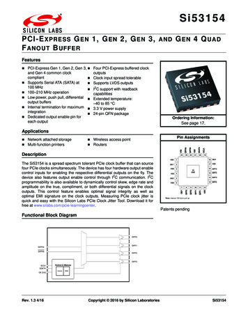
Si53154PCI-E XPRESS G EN 1, G EN 2, G EN 3, AND G EN 4 Q UADF ANOUT B UFFERFeatures PCI-Express Gen 1, Gen 2, Gen 3, and Gen 4 common clockcompliant Supports Serial ATA (SATA) at 100 MHz 100–210 MHz operationLow power, push pull, differential output buffersInternal termination for maximum integration Dedicated output enable pin foreach outputFour PCI-Express buffered clockoutputsClock input spread tolerableSupports LVDS outputsI2C support with readbackcapabilitiesExtended temperature:–40 to 85 C3.3 V power supply24-pin QFN packageOrdering Information:See page 17.Applications24222120SCLK19VDD118 OE3*OE1*217 VDDVDD3VSS4OE2*5VDD616 DIFF325GND15 DIFF314 DIFF289101112DIFF0DIFF0DIFF1DIFF1VDD13 DIFF27OE0*The Si53154 is a spread spectrum tolerant PCIe clock buffer that can sourcefour PCIe clocks simultaneously. The device has four hardware output enablecontrol inputs for enabling the respective differential outputs on the fly. Thedevice also features output enable control through I2C communication. I2Cprogrammability is also available to dynamically control skew, edge rate andamplitude on the true, compliment, or both differential signals on the clockoutputs. This control feature enables optimal signal integrity as well asoptimal EMI signature on the clock outputs. Measuring PCIe clock jitter isquick and easy with the Silicon Labs PCIe Clock Jitter Tool. Download it forfree at nSDATAWireless access point RoutersDIFFINPin Assignments VSSNetwork attached storage Multi-function printersDIFFIN *Note: Internal 100 kohm pull-up.Patents pendingFunctional Block ntrol & MemoryControlRAMOE [3:0]Rev. 1.3 4/16Copyright 2016 by Silicon LaboratoriesSi53154
Si531542Rev. 1.3
Si53154TABLE O F C ONTENTSSectionPage1. Electrical Specifications . . . . . . . . . . . . . . . . . . . . . . . . . . . . . . . . . . . . . . . . . . . . . . . . . . .42. Functional Description . . . . . . . . . . . . . . . . . . . . . . . . . . . . . . . . . . . . . . . . . . . . . . . . . . . .72.1. OE Pin Definition . . . . . . . . . . . . . . . . . . . . . . . . . . . . . . . . . . . . . . . . . . . . . . . . . . . . .72.2. OE Assertion . . . . . . . . . . . . . . . . . . . . . . . . . . . . . . . . . . . . . . . . . . . . . . . . . . . . . . . .72.3. OE Deassertion . . . . . . . . . . . . . . . . . . . . . . . . . . . . . . . . . . . . . . . . . . . . . . . . . . . . . .73. Test and Measurement Setup . . . . . . . . . . . . . . . . . . . . . . . . . . . . . . . . . . . . . . . . . . . . . . .84. Control Registers . . . . . . . . . . . . . . . . . . . . . . . . . . . . . . . . . . . . . . . . . . . . . . . . . . . . . . . .104.1. I2C Interface . . . . . . . . . . . . . . . . . . . . . . . . . . . . . . . . . . . . . . . . . . . . . . . . . . . . . . . 104.2. Data Protocol . . . . . . . . . . . . . . . . . . . . . . . . . . . . . . . . . . . . . . . . . . . . . . . . . . . . . .105. Pin Descriptions: 24-Pin QFN . . . . . . . . . . . . . . . . . . . . . . . . . . . . . . . . . . . . . . . . . . . . . . 156. Ordering Guide . . . . . . . . . . . . . . . . . . . . . . . . . . . . . . . . . . . . . . . . . . . . . . . . . . . . . . . . . . 177. Package Outline . . . . . . . . . . . . . . . . . . . . . . . . . . . . . . . . . . . . . . . . . . . . . . . . . . . . . . . . . 188. Land Pattern . . . . . . . . . . . . . . . . . . . . . . . . . . . . . . . . . . . . . . . . . . . . . . . . . . . . . . . . . . . . 19Document Change List . . . . . . . . . . . . . . . . . . . . . . . . . . . . . . . . . . . . . . . . . . . . . . . . . . . . .21Rev. 1.33
Si531541. Electrical SpecificationsTable 1. DC Electrical SpecificationsParameterSymbolTest ConditionMinTypMaxUnit3.3 V Operating VoltageVDD core3.3 5%3.135—3.465V3.3 V Input High VoltageVIHControl input pins2.0—VDD 0.3V3.3 V Input Low VoltageVILControl input pinsVSS – 0.3—0.8VInput High VoltageVIHI2CSDATA, SCLK2.2—–VInput Low VoltageVILI2CSDATA, SCLK——1.0VInput High Leakage CurrentIIHExcept internal pull-downresistors, 0 VIN VDD——5 AInput Low Leakage CurrentIILExcept internal pull-upresistors, 0 VIN VDD–5—— A3.3 V Output High Voltage(Single-Ended Outputs)VOHIOH –1 mA2.4——V3.3 V Output Low Voltage(Single-Ended Outputs)VOLIOL 1 mA——0.4VHigh-impedance OutputCurrentIOZ–10—10 AInput Pin �—35mAOutput Pin CapacitancePin InductanceDynamic Supply Current inFanout Mode4IDD 3.3VDifferential clocks with 5”traces and 2 pF load,frequency at 100 MHzRev. 1.3
Si53154Table 2. AC Electrical t100—210MHz0.6—4V/nsDIFFIN at 0.7 VInput Frequency RangeRising and Falling SlewRates for Each Clock OutputSignal in a Given DifferentialPairfinTR / TFSingle ended measurement: VOL 0.175 to VOH 0.525 V (Averaged)Differential Input HighVoltageVIH150——mVDifferential Input LowVoltageVIL——–150mVCrossing Point Voltage at0.7 V SwingVOXSingle-ended measurement250—550mVVcross Variation over allEdges VOXSingle-ended ��—psAbsolute Maximum InputVoltageVMAX——1.15VAbsolute Minimum InputVoltageVMIN–0.3——VDuty Cycle for Each ClockOutput Signal in a GivenDifferential PairTDCMeasured at crossing point VOX45—55%Rise/Fall MatchingTRFMDetermined as a fraction of2 x (TR – TF)/(TR TF)——20%Duty CycleTDCMeasured at 0 V differential45—55%Clock SkewTSKEWMeasured at 0 V differential——50psAdditive Peak JitterPk-Pk0—10ps10 kHz F 1.5 MHz0—0.5ps1.5 MHz F Nyquist Rate0—0.5psIncludes PLL BW 2–4 MHz(CDR 10 MHz)0—0.10psDifferential Ringback VoltageTime before RingbackAllowedDIFF at 0.7 VAdditive PCIe Gen 2 PhaseJitterRMSGEN2Additive PCIe Gen 3 PhaseJitterRMSGEN3Notes:1. Gen 4 specifications based on the PCI-Express Base Specification 4.0 rev. 0.5.2. Download the Silicon Labs PCIe Clock Jitter Tool at www.silabs.com/pcie-learningcenter.Rev. 1.35
Si53154Table 2. AC Electrical Specifications ditive PCIe Gen 4 PhaseJitterRMSGEN4PCIe Gen 4——0.10psAdditive Cycle to Cycle JitterTCCJMeasured at 0 V differential—2050psLong-term AccuracyLACCMeasured at 0 V differential——100ppmRising/Falling Slew rateTR/TFMeasured differentially from 150 ing Point Voltage at0.7 V SwingVOXEnable/Disable and SetupClock Stabilization fromPower-UpTSTABLEStopclock Set-up TimeTSSMeasured from the point when bothVDD and clock input are validNotes:1. Gen 4 specifications based on the PCI-Express Base Specification 4.0 rev. 0.5.2. Download the Silicon Labs PCIe Clock Jitter Tool at www.silabs.com/pcie-learningcenter.Table 3. Absolute Maximum ConditionsParameterSymbolConditionMinTypMaxUnitVDD 3.3VFunctional——4.6VInput VoltageVINRelative to VSS–0.5—4.6VDCTemperature, StorageTSNon-functional–65—150 CIndustrial Temperature, OperatingAmbientTAFunctional–40—85 CCommercial Temperature, OperatingAmbientTAFunctional0—85 CTemperature, JunctionTJFunctional——150 CDissipation, Junction to CaseØJCJEDEC (JESD 51)——25 C/WDissipation, Junction to AmbientØJAJEDEC (JESD 51)——37 C/WESDHBMJEDEC (JESD 22 - A114)2000—–VUL-94UL (Class)Main Supply VoltageESD Protection (Human Body Model)Flammability RatingV–0Note: Multiple Supplies: The voltage on any input or I/O pin cannot exceed the power pin during power-up. Power supplysequencing is not required.6Rev. 1.3
Si531542. Functional Description2.1. OE Pin DefinitionThe OE pins are active high inputs used to enable and disable the output clocks. To enable the output clock, the OEpin needs to be logic high and the I2C output enable bit needs to be logic high. There are two methods to disablethe output clocks: the OE is pulled to a logic low, or the I2C enable bit is set to a logic low. The OE pins are requiredto be driven at all times even though they have an internal 100 k resistor.2.2. OE AssertionThe OE signals are active high inputs used for synchronous stopping and starting the DIFF output clocks respectivelywhile the rest of the clock generator continues to function. The assertion of the OE signal by making it logic highcauses stopped respective DIFF outputs to resume normal operation. No short or stretched clock pulses areproduced when the clock resumes. The maximum latency from the assertion to active outputs is no more than twoto six output clock cycles.2.3. OE DeassertionWhen the OE pin is deasserted by making it logic low, the corresponding DIFF output is stopped, and the final outputstate is driven low.Rev. 1.37
Si531543. Test and Measurement SetupFigures 1–3 show the test load configuration for differential clock signals.Figure 1. 0.7 V Differential Load ConfigurationFigure 2. Differential Measurement for Differential Output Signals(for AC Parameters Measurement)8Rev. 1.3
Si53154VMIN –0.30VVMIN –0.30VFigure 3. Single-Ended Measurement for Differential Output Signals(for AC Parameters Measurement)Rev. 1.39
Si531544. Control Registers4.1. I2C InterfaceTo enhance the flexibility and function of the clock buffer, an I2C interface is provided. Through the I2C Interface,various device functions are available, such as individual clock output enable. The registers associated with the I2CInterface initialize to their default setting at power-up. The use of this interface is optional. Clock device registerchanges are normally made at system initialization, if any are required. Power management functions can only beprogramed in program mode and not in normal operation modes.4.2. Data ProtocolThe I2C protocol accepts byte write, byte read, block write, and block read operations from the controller. For blockwrite/read operation, access the bytes in sequential order from lowest to highest (most significant bit first) with theability to stop after any complete byte is transferred. For byte write and byte read operations, the system controllercan access individually indexed bytes.The block write and block read protocol is outlined in Table 4 while Table 5 outlines byte write and byte readprotocol. The slave receiver address is 11010110 (D6h).Table 4. Block Read and Block Write lock Write ProtocolDescriptionStartSlave address–7 bitsWriteAcknowledge from slaveCommand Code–8 bitsAcknowledge from slaveByte Count–8 bitsAcknowledge from slaveData byte 1–8 bitsAcknowledge from slaveData byte 2–8 bitsAcknowledge from slaveData Byte/Slave AcknowledgesData Byte N–8 bitsAcknowledge from 755:4856.Rev. 1.3Block Read ProtocolDescriptionStartSlave address–7 bitsWriteAcknowledge from slaveCommand Code–8 bitsAcknowledge from slaveRepeat startSlave address–7 bitsRead 1Acknowledge from slaveByte Count from slave–8 bitsAcknowledgeData byte 1 from slave–8 bitsAcknowledgeData byte 2 from slave–8 bitsAcknowledgeData bytes from slave/AcknowledgeData Byte N from slave–8 bitsNOT AcknowledgeStop
Si53154Table 5. Byte Read and Byte Write ProtocolBit18:291018:111927:202829Byte Write ProtocolDescriptionStartSlave address–7 bitsWriteAcknowledge from slaveCommand Code–8 bitsAcknowledge from slaveData byte–8 bitsAcknowledge from slaveStopBit18:291018:11192027:21282937:303839Rev. 1.3Byte Read ProtocolDescriptionStartSlave address–7 bitsWriteAcknowledge from slaveCommand Code–8 bitsAcknowledge from slaveRepeated startSlave address–7 bitsReadAcknowledge from slaveData from slave–8 bitsNOT AcknowledgeStop11
Si53154Control Register 0. Byte NameTypeReset settings 00000000BitNameFunction7:0ReservedControl Register 1. Byte 1BitD7D6D5D4D3NameTypeDIFF0 OER/WR/WR/WR/WR/WReset settings 00000101BitName7:3Reserved2DIFF0 OEFunctionOutput Enable for DIFF0.0: Output disabled.1: Output enabled.1Reserved0DIFF1 OEOutput Enable for DIFF1.0: Output disabled.1: Output enabled.12Rev. 1.3R/WDIFF1 OER/WR/W
Si53154Control Register 2. Byte 2 OE DIFF3 OER/WR/WReset settings 11000000BitNameFunction7DIFF2 OEOutput Enable for DIFF2.0: Output disabled.1: Output enabled.6DIFF3 OEOutput Enable for DIFF3.0: Output disabled.1: Output enabled.5:0ReservedControl Register 3. Byte 3BitD7D6D5D4D3D2D1D0NameRev CodeBit 3Rev CodeBit 2Rev CodeBit 1Rev CodeBit 0Vendor IDbit 3Vendor IDbit 2Vendor IDbit 1Vendor IDbit 0TypeR/WR/WR/WR/WR/WR/WR/WR/WReset settings 00001000BitNameFunction7:4Rev Code Bit 3:0Program Revision Code.3:0Vendor ID bit 3:0Vendor Identification Code.Control Register 4. Byte peR/WR/WR/WR/WR/WR/WR/WR/WReset settings 00000110BitName7:0BC7:0FunctionByte Count Register.Rev. 1.313
Si53154Control Register 5. Byte 5BitD7D6D5D4D3D2D1D0R/WR/WR/WR/WName DIFF Amp Sel DIFF Amp Cntl[2] DIFF Amp Cntl[1] DIFF Amp Cntl[0]TypeR/WR/WR/WR/WReset settings 11011000BitName7DIFF Amp SelFunctionAmplitude Control for DIFF Differential Outputs.0: Differential outputs with Default amplitude.1: Differential outputs amplitude is set by Byte 5[6:4].146DIFF Amp Cntl[2]5DIFF Amp Cntl[1]4DIFF Amp Cntl[0]3:0ReservedDIFF Differential Outputs Amplitude Adjustment.000: 300 mV 001: 400 mV 010: 500 mV100: 700 mV 101: 800 mV 110: 900 mVRev. 1.3011: 600 mV111: 1000 mV
Si531542423222120SCLKSDATAVDDDIFFINDIFFINVSS5. Pin Descriptions: 24-Pin QFN19VDD118 OE3*OE1*217 VDDVDD3VSS4OE2*5VDD616 DIFF325GND15 DIFF314 DIFF2789101112OE0*DIFF0DIFF0DIFF1DIFF1VDD13 DIFF2*Note: Internal 100 kohm pull-up.Figure 4. 24-Pin QFNTable 6. Si53154 24-Pin QFN DescriptionsPin #NameTypeDescription1VDDPWR 3.3 V power supply.2OE1I,PU3VDDPWR 3.3 V power supply.4VSSGNDGround.5OE2I,PUActive high input pin enables DIFF2 (internal 100 k pull-up).Refer to Table 1 on page 4 for OE specifications.6VDDPWR 3.3 V power supply.7OE0I,PU8DIFF0O, DIF 0.7 V, differential clock output.9DIFF0O, DIF 0.7 V, differential clock output.10DIFF1O, DIF 0.7 V, differential clock output.11DIFF1O, DIF 0.7 V, differential clock output.12VDD13DIFF2Active high input pin enables DIFF1 (internal 100 k pull-up).Refer to Table 1 on page 4 for OE specifications.Active high input pin enables DIFF0 (internal 100 k pull-up).Refer to Table 1 on page 4 for OE specifications.PWR 3.3 V power supply.O, DIF 0.7 V, differential clock output.Rev. 1.315
Si53154Table 6. Si53154 24-Pin QFN DescriptionsPin #Name14DIFF2O, DIF 0.7 V, differential clock output.15DIFF3O, DIF 0.7 V, differential clock output.16DIFF3O, DIF 0.7 V, differential clock output.17VDDPWR 3.3 V power supply.18OE3I,PU19SCLKI20SDATAI/O21VDD22DIFFINI0.7 V Differential True Input, typically 100 MHz. Input frequency range100 to 210 MHz.23DIFFINO0.7 V Differential Complement Input, typically 100 MHz. Input frequencyrange 100 to 210 MHz.24VSSGNDGround.25GNDGNDGround for bottom pad of the IC.16TypeDescriptionActive high input pin enables DIFF3 (internal 100 k pull-up).Refer to Table 1 on page 4 for OE specifications.SMBus compatible SCLOCK.SMBus compatible SDATA.PWR 3.3 V power supply.Rev. 1.3
Si531546. Ordering GuidePart NumberPackage TypeTemperatureSi53154-A01AGM24-pin QFNExtended, –40 to 85 CSi53154-A01AGMR24-pin QFN—Tape and ReelExtended, –40 to 85 CLead-freeRev. 1.317
Si531547. Package OutlineFigure 5 illustrates the package details for the Si53154. Table 7 lists the values for the dimensions shown in theillustration.Figure 5. 24-Pin Quad Flat No Lead (QFN) PackageTable 7. Package Diagram 10.000.0250.05b0.200.250.30DD24.00 BSC2.602.70e0.50 BSCE4.00 c0.08ddd0.07Notes:1. All dimensions shown are in millimeters (mm) unless otherwisenoted.2. Dimensioning and Tolerancing per ANSI Y14.5M-1994.3. This drawing conforms to JEDEC outline MO-220, variation VGGD-84. Recommended card reflow profile is per the JEDEC/IPC J-STD-020specification for Small Body Components18Rev. 1.3
Si531548. Land PatternFigure 6 illustrates the recommended land pattern details for the Si53154 in a 24-pin QFN package. Table 8 liststhe values for the dimensions shown in the illustration.Figure 6. Land PatternRev. 1.319
Si53154Table 8. PCB Land Pattern DimensionsDimensionUnit mmC14.0C24.0E0.50 BSCX10.30X22.70Y10.80Y22.70Notes:General1. All dimensions shown are in millimeters (mm).2. This Land Pattern Design is based on the IPC-7351 guidelines.Solder Mask Design1. All metal pads are to be non-solder mask defined (NSMD). Clearance between thesolder mask and the metal pad is to be 60 m minimum, all the way around the pad.Stencil Design1. A stainless steel, laser-cut and electro-polished stencil with trapezoidal wallsshould be used to assure good solder paste release.2. The stencil thickness should be 0.125mm (5 mils).3. The ratio of stencil aperture to land pad size should be 1:1 for all perimeter pads.4. A 2x2 array of 1.10mm x 1.10mm openings on 1.30mm pitch should be used forthe center ground pad.Card Assembly1. A No-Clean, Type-3 solder paste is recommended.2. The recommended card reflow profile is per the JEDEC/IPC J-STD-020specification for Small Body Components.20Rev. 1.3
Si53154DOCUMENT CHANGE LISTRevision 0.1 to Revision 1.0 Updated Features and Description.Updated Table 2. Updated Table 3. Updated Section 4.1. Revision 1.0 to Revision 1.1 Updated Features on page 1 Updated Description on page 1. Updated specs in Table 2, “AC ElectricalSpecifications,” on page 5. Added Land PatternRevision 1.1 to Revision 1.2 Added condition for Clock Stabilization from Powerup, TSTABLE, in Table 2.Revision 1.2 to Revision 1.3 Updated Theta JC to 25 C/W.Rev. 1.321
ClockBuilder ProOne-click access to Timing tools,documentation, software, sourcecode libraries & more. Available forWindows and iOS (CBGo only).www.silabs.com/CBProTiming CBProQualitywww.silabs.com/qualitySupport and Communitycommunity.silabs.comDisclaimerSilicon Laboratories intends to provide customers with the latest, accurate, and in-depth documentation of all peripherals and modules available for system and software implementers usingor intending to use the Silicon Laboratories products. Characterization data, available modules and peripherals, memory sizes and memory addresses refer to each specific device, and"Typical" parameters provided can and do vary in different applications. Application examples described herein are for illustrative purposes only. Silicon Laboratories reserves the right tomake changes without further notice and limitation to product information, specifications, and descriptions herein, and does not give warranties as to the accuracy or completeness of theincluded information. Silicon Laboratories shall have no liability for the consequences of use of the information supplied herein. This document does not imply or express copyright licensesgranted hereunder to design or fabricate any integrated circuits. The products are not designed or authorized to be used within any Life Support System without the specific written consentof Silicon Laboratories. A "Life Support System" is any product or system intended to support or sustain life and/or health, which, if it fails, can be reasonably expected to result in significantpersonal injury or death. Silicon Laboratories products are not designed or authorized for military applications. Silicon Laboratories products shall under no circumstances be used inweapons of mass destruction including (but not limited to) nuclear, biological or chemical weapons, or missiles capable of delivering such weapons.Trademark InformationSilicon Laboratories Inc. , Silicon Laboratories , Silicon Labs , SiLabs and the Silicon Labs logo , Bluegiga , Bluegiga Logo , Clockbuilder , CMEMS , DSPLL , EFM , EFM32 ,EFR, Ember , Energy Micro, Energy Micro logo and combinations thereof, "the world’s most energy friendly microcontrollers", Ember , EZLink , EZRadio , EZRadioPRO , Gecko ,ISOmodem , Precision32 , ProSLIC , Simplicity Studio , SiPHY , Telegesis, the Telegesis Logo , USBXpress and others are trademarks or registered trademarks of Silicon Laboratories Inc. ARM, CORTEX, Cortex-M3 and THUMB are trademarks or registered trademarks of ARM Holdings. Keil is a registered trademark of ARM Limited. All other products or brandnames mentioned herein are trademarks of their respective holders.Silicon Laboratories Inc.400 West Cesar ChavezAustin, TX 78701USAhttp://www.silabs.com
PCI-Express Gen 1, Gen 2, Gen 3, and Gen 4 common clock compliant Supports Serial ATA (SATA) at 100 MHz 100-210 MHz operation Low power, push pull, differential output buffers Internal termination for maximum integration Dedicated output enable pin for each output Four PCI-Express buffered clock outputs


![PCI Compliant - but are we secure -- FOR PRINTING IN GRAYSCALE [Read-Only]](/img/14/303-pci-3.jpg)