Transcription
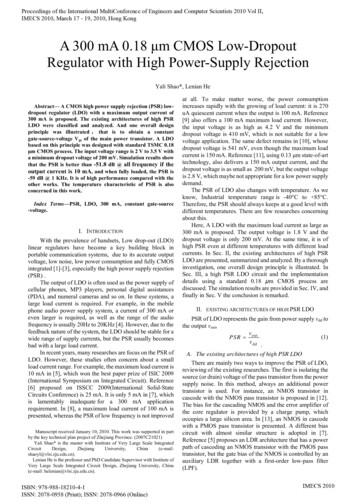
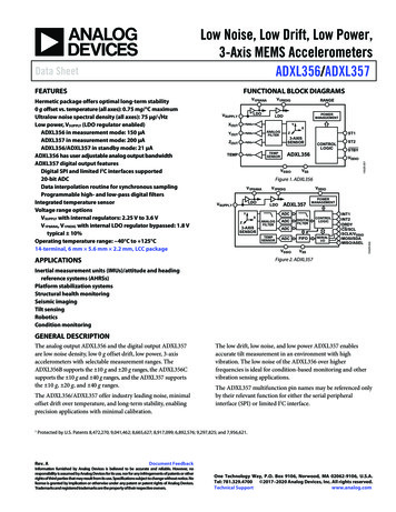
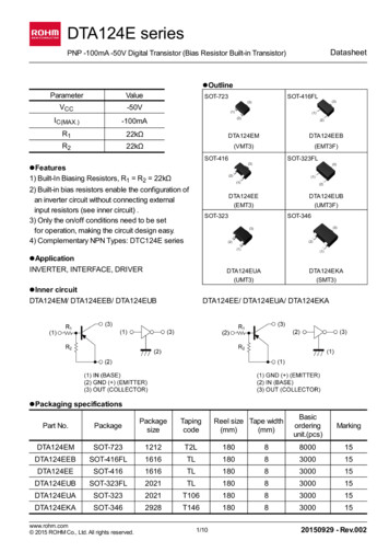
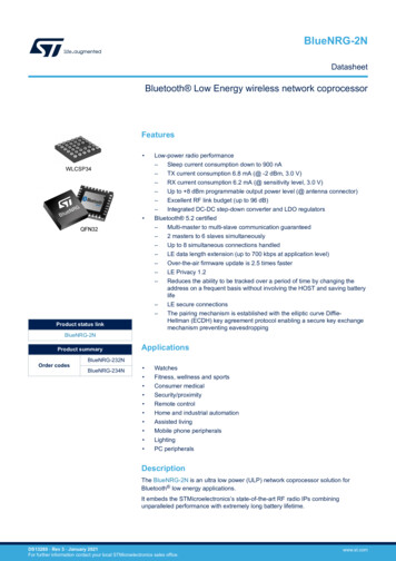
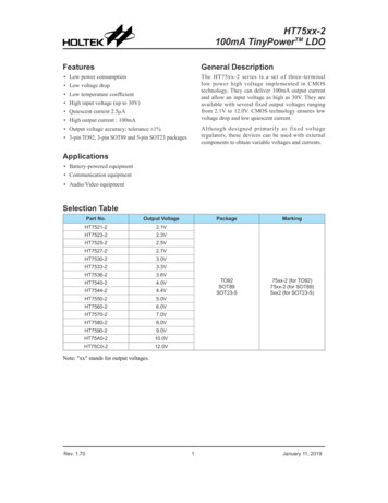
HT75xx-2100mA TinyPowerTM LDOFeaturesGeneral Description Low power consumptionThe HT75xx-2 series is a set of three-terminallow power high voltage implemented in CMOStechnology. They can deliver 100mA output currentand allow an input voltage as high as 30V. They areavailable with several fixed output voltages rangingfrom 2.1V to 12.0V. CMOS technology ensures lowvoltage drop and low quiescent current. Low voltage drop Low temperature coefficient High input voltage (up to 30V) Quiescent current 2.5μA High output current : 100mAAlthough designed primarily as fixed voltageregulators, these devices can be used with externalcomponents to obtain variable voltages and currents. Output voltage accuracy: tolerance 1% 3-pin TO92, 3-pin SOT89 and 5-pin SOT23 packagesApplications Battery-powered equipment Communication equipment Audio/Video equipmentSelection TablePart No.Output VPackageMarkingTO92SOT89SOT23-575xx-2 (for TO92)75xx-2 (for SOT89)5xx2 (for SOT23-5)Note: ″xx″ stands for output voltages.Rev. 1.701January 11, 2019
HT75xx-2Block Diagram Pin Assignment Absolute Maximum Ratings Supply Voltage . 0.3V to 33VOperating Temperature . 40 C to 85 CStorage Temperature . 50 C to 160 CMaximum Junction Temperature. 150 CNote: These are stress ratings only. Stresses exceeding the range specified under ″AbsolutemAximum Ratings″may cause substantial damage to the device. Functional operation of this device at other conditions beyondthose listed in the specification is not implied and prolonged exposure to extreme conditionsmAy affectdevice reliability.Thermal InformationSymbolθJAPDParameterThermal Resistance (Junction to Ambient)(Assume no ambient airflow, no heat sink)Power DissipationPackageMax.UnitSOT23-5500 C/WSOT89200 C/WTO92200 C/WSOT23-50.20WSOT890.50WTO920.50WNote: PD is measured at Ta 25 CRev. 1.702January 11, 2019
HT75xx-2Pin DescriptionsPin No.Pin NamePin Description1GNDGround pin2VINInput pin3VOUTOutput pinElectrical CharacteristicsHT7521-2, 2.1V Output TypeSymbolTa 25 CTest 2.0792.1002.121VVINInput VoltageVOUTOutput VoltageVIN 4.1V, IOUT 10mAIOUTOutput CurrentVIN 4.1V70100—mA VOUTLoad RegulationVIN 4.1V, 1mA IOUT 50mA—2560mVVDIFDropout Voltage (Note)IOUT 1mA, VOUT 2%—30100mVISSQuiescent CurrentNo load—2.54.0μALine Regulation3.1V VIN 30V, IOUT 1mA——0.2%/VTemperature CoefficientIOUT 10mA, -40 C Ta 85 C—100—ppm/ C —Min.Note: Dropout voltage is defined as the input voltage minus the output voltage that produces a 2% change in theoutput voltage from the value at VIN VOUT 2V with a fixed load.HT7523-2, 2.3V Output TypeSymbolTa 25 CTest 2.2772.3002.323VVINInput VoltageVOUTOutput VoltageVIN 4.3V, IOUT 10mAIOUTOutput CurrentVIN 4.3V70100—mA VOUTLoad RegulationVIN 4.3V, 1mA IOUT 50mA—2560mVVDIFDropout VoltageIOUT 1mA, VOUT 2%—30100mVISSQuiescent CurrentNo load—2.54.0μALine Regulation3.3V VIN 30V, IOUT 1mA——0.2%/VTemperature CoefficientIOUT 10mA, -40 C Ta 85 C—100—ppm/ C —Min.(Note)Note: Dropout voltage is defined as the input voltage minus the output voltage that produces a 2% change in theoutput voltage from the value at VIN VOUT 2V with a fixed load.Rev. 1.703January 11, 2019
HT75xx-2HT7525-2, 2.5V Output TypeTa 25 CSymbolTest 2.4752.5002.525VVINInput VoltageVOUTOutput VoltageVIN 4.5V, IOUT 10mAIOUTOutput CurrentVIN 4.5V70100—mA VOUTLoad RegulationVIN 4.5V, 1mA IOUT 50mA—2560mVVDIFDropout Voltage (Note)IOUT 1mA, VOUT 2%—30100mVISSQuiescent CurrentNo load—2.54.0μALine Regulation3.5V VIN 30V, IOUT 1mA——0.2%/VTemperature CoefficientIOUT 10mA, -40 C Ta 85 C—100—ppm/ C —Min.Note: Dropout voltage is defined as the input voltage minus the output voltage that produces a 2% change in theoutput voltage from the value at VIN VOUT 2V with a fixed load.HT7527-2, 2.7V Output TypeTa 25 CSymbolTest 2.6732.7002.727VVINInput VoltageVOUTOutput VoltageVIN 4.7V, IOUT 10mAIOUTOutput CurrentVIN 4.7V70100—mA VOUTLoad RegulationVIN 4.7V, 1mA IOUT 50mA—2560mVVDIFDropout Voltage (Note)IOUT 1mA, VOUT 2%—30100mVISSQuiescent CurrentNo load—2.54.0μALine Regulation3.7V VIN 30V, IOUT 1mA——0.2%/VTemperature CoefficientIOUT 10mA, -40 C Ta 85 C—100—ppm/ C —Min.Note: Dropout voltage is defined as the input voltage minus the output voltage that produces a 2% change in theoutput voltage from the value at VIN VOUT 2V with a fixed load.Rev. 1.704January 11, 2019
HT75xx-2HT7530-2, 3.0V Output TypeTa 25 CSymbolTest 2.9703.0003.030VVINInput VoltageVOUTOutput VoltageVIN 5.0V, IOUT 10mAIOUTOutput CurrentVIN 5.0V70100—mA VOUTLoad RegulationVIN 5.0V, 1mA IOUT 50mA—2560mVVDIFDropout Voltage (Note)IOUT 1mA, VOUT 2%—30100mVISSQuiescent CurrentNo load—2.54.0μALine Regulation4.0V VIN 30V, IOUT 1mA——0.2%/VTemperature CoefficientIOUT 10mA, -40 C Ta 85 C—100—ppm/ C —Min.Note: Dropout voltage is defined as the input voltage minus the output voltage that produces a 2% change in theoutput voltage from the value at VIN VOUT 2V with a fixed load.HT7533-2, 3.3V Output TypeTa 25 CSymbolTest 3.2673.3003.333VVINInput VoltageVOUTOutput VoltageVIN 5.3V, IOUT 10mAIOUTOutput CurrentVIN 5.3V70100—mA VOUTLoad RegulationVIN 5.3V, 1mA IOUT 50mA—2560mVVDIFDropout Voltage (Note)IOUT 1mA, VOUT 2%—2555mVISSQuiescent CurrentNo load—2.54.0μALine Regulation4.3V VIN 30V, IOUT 1mA——0.2%/VTemperature CoefficientIOUT 10mA, -40 C Ta 85 C—100—ppm/ C —Min.Note: Dropout voltage is defined as the input voltage minus the output voltage that produces a 2% change in theoutput voltage from the value at VIN VOUT 2V with a fixed load.Rev. 1.705January 11, 2019
HT75xx-2HT7536-2, 3.6V Output TypeTa 25 CSymbolTest 3.5643.6003.636VVINInput VoltageVOUTOutput VoltageVIN 5.6V, IOUT 10mAIOUTOutput CurrentVIN 5.6V70100—mA VOUTLoad RegulationVIN 5.6V, 1mA IOUT 50mA—2560mVVDIFDropout Voltage (Note)IOUT 1mA, VOUT 2%—2555mVISSQuiescent CurrentNo load—2.54.0μALine Regulation4.6V VIN 30V, IOUT 1mA——0.2%/VTemperature CoefficientIOUT 10mA, -40 C Ta 85 C—100—ppm/ C —Min.Note: Dropout voltage is defined as the input voltage minus the output voltage that produces a 2% change in theoutput voltage from the value at VIN VOUT 2V with a fixed load.HT7540-2, 4.0V Output TypeTa 25 CSymbolTest 3.9604.0004.040VVINInput VoltageVOUTOutput VoltageVIN 6.0V, IOUT 10mAIOUTOutput CurrentVIN 6.0V70100—mA VOUTLoad RegulationVIN 6.0V, 1mA IOUT 50mA—2560mVVDIFDropout Voltage (Note)IOUT 1mA, VOUT 2%—2555mVISSQuiescent CurrentNo load—2.54.0μALine Regulation5.0V VIN 30V, IOUT 1mA——0.2%/VTemperature CoefficientIOUT 10mA, -40 C Ta 85 C—100—ppm/ C —Min.Note: Dropout voltage is defined as the input voltage minus the output voltage that produces a 2% change in theoutput voltage from the value at VIN VOUT 2V with a fixed load.Rev. 1.706January 11, 2019
HT75xx-2HT7544-2, 4.4V Output TypeTa 25 CSymbolTest 4.3564.4004.444VVINInput VoltageVOUTOutput VoltageVIN 6.4V, IOUT 10mAIOUTOutput CurrentVIN 6.4V70100—mA VOUTLoad RegulationVIN 6.4V, 1mA IOUT 50mA—2560mVVDIFDropout Voltage (Note)IOUT 1mA, VOUT 2%—2555mVISSQuiescent CurrentNo load—2.54.0μALine Regulation5.4V VIN 30V, IOUT 1mA——0.2%/VTemperature CoefficientIOUT 10mA, -40 C Ta 85 C—100—ppm/ C —Min.Note: Dropout voltage is defined as the input voltage minus the output voltage that produces a 2% change in theoutput voltage from the value at VIN VOUT 2V with a fixed load.HT7550-2, 5.0V Output TypeTa 25 CSymbolTest .0005.050V100150—mAVIN 7.0V, 1mA IOUT 70mA—2560mVIOUT 1mA, VOUT 2%—2555mVConditionsVINInput VoltageVOUTOutput VoltageVIN 7.0V, IOUT 10mAIOUTOutput CurrentVIN 7.0V VOUTLoad RegulationVDIFDropout VoltageISSQuiescent CurrentNo load—2.54.0μALine Regulation6.0V VIN 30V, IOUT 1mA——0.2%/VTemperature CoefficientIOUT 10mA, -40 C Ta 85 C—100—ppm/ C —(Note)Note: Dropout voltage is defined as the input voltage minus the output voltage that produces a 2% change in theoutput voltage from the value at VIN VOUT 2V with a fixed load.Rev. 1.707January 11, 2019
HT75xx-2HT7560-2, 6.0V Output TypeTa 25 CSymbolTest .0006.060V150——mAVIN 8.0V, 1mA IOUT 70mA—2560mVIOUT 1mA, VOUT 2%—2555mVConditionsVINInput VoltageVOUTOutput VoltageVIN 8.0V, IOUT 10mAIOUTOutput CurrentVIN 8.0V VOUTLoad RegulationVDIFDropout VoltageISSQuiescent CurrentNo load—2.54.0μALine Regulation7.0V VIN 30V, IOUT 1mA—0.2—%/VTemperature CoefficientIOUT 10mA, -40 C Ta 85 C—100—ppm/ C —(Note)Note: Dropout voltage is defined as the input voltage minus the output voltage that produces a 2% change in theoutput voltage from the value at VIN VOUT 2V with a fixed load.HT7570-2, 7.0V Output TypeTa 25 CSymbolTest .0007.070V150——mAVIN 9.0V, 1mA IOUT 70mA—2560mVIOUT 1mA, VOUT 2%—2555mVConditionsVINInput VoltageVOUTOutput VoltageVIN 9.0V, IOUT 10mAIOUTOutput CurrentVIN 9.0V VOUTLoad RegulationVDIFDropout VoltageISSQuiescent CurrentNo load—2.54.0μALine Regulation8.0V VIN 30V, IOUT 1mA—0.2—%/VTemperature CoefficientIOUT 10mA, -40 C Ta 85 C—100—ppm/ C —(Note)Note: Dropout voltage is defined as the input voltage minus the output voltage that produces a 2% change in theoutput voltage from the value at VIN VOUT 2V with a fixed load.Rev. 1.708January 11, 2019
HT75xx-2HT7580-2, 8.0V Output TypeTa 25 CSymbolTest .0008.080V150——mAVIN 10.0V, 1mA IOUT 70mA—2560mVIOUT 1mA, VOUT 2%—2555mVConditionsVINInput VoltageVOUTOutput VoltageVIN 10.0V, IOUT 10mAIOUTOutput CurrentVIN 10.0V VOUTLoad RegulationVDIFDropout VoltageISSQuiescent CurrentNo load—2.54.0μALine Regulation9.0V VIN 30V, IOUT 1mA—0.2—%/VTemperature CoefficientIOUT 10mA, -40 C Ta 85 C—100—ppm/ C —(Note)Note: Dropout voltage is defined as the input voltage minus the output voltage that produces a 2% change in theoutput voltage from the value at VIN VOUT 2V with a fixed load.HT7590-2, 9.0V Output TypeTa 25 CSymbolTest .0009.090V150——mAVIN 11.0V, 1mA IOUT 70mA—2570mVIOUT 1mA, VOUT 2%—2555mVConditionsVINInput VoltageVOUTOutput VoltageVIN 11.0V, IOUT 10mAIOUTOutput CurrentVIN 11.0V VOUTLoad RegulationVDIFDropout VoltageISSQuiescent CurrentNo load—2.54.0μALine Regulation10.0V VIN 30V, IOUT 1mA—0.2—%/VTemperature CoefficientIOUT 10mA, -40 C Ta 85 C—100—ppm/ C —(Note)Note: Dropout voltage is defined as the input voltage minus the output voltage that produces a 2% change in theoutput voltage from the value at VIN VOUT 2V with a fixed load.Rev. 1.709January 11, 2019
HT75xx-2HT75A0-2, 10.0V Output TypeTa 25 CSymbolTest 9.90010.00010.100V150——mAVINInput VoltageVOUTOutput VoltageVIN 12.0V, IOUT 10mAIOUTOutput CurrentVIN 12.0V VOUTLoad RegulationVIN 12.0V, 1mA IOUT 70mA—2570mVVDIFDropout Voltage (Note)IOUT 1mA, VOUT 2%—2555mVISSQuiescent CurrentNo load—2.54.0μALine Regulation11.0V VIN 30V, IOUT 1mA—0.2—%/VTemperature CoefficientIOUT 10mA, -40 C Ta 85 C—100—ppm/ C —Min.Note: Dropout voltage is defined as the input voltage minus the output voltage that produces a 2% change in theoutput voltage from the value at VIN VOUT 2V with a fixed load.HT75C0-2, 12.0V Output TypeTa 25 CSymbolTest 11.88012.00012.120V150——mAVINInput VoltageVOUTOutput VoltageVIN 14.0V, IOUT 10mAIOUTOutput CurrentVIN 14.0V VOUTLoad RegulationVIN 14.0V, 1mA IOUT 70mA—2570mVVDIFDropout Voltage (Note)IOUT 1mA, VOUT 2%—2555mVISSQuiescent CurrentNo load—2.54.0μALine Regulation13.0V VIN 30V, IOUT 1mA—0.2—%/VTemperature CoefficientIOUT 10mA, -40 C Ta 85 C—100—ppm/ C —Min.Note: Dropout voltage is defined as the input voltage minus the output voltage that produces a 2% change in theoutput voltage from the value at VIN VOUT 2V with a fixed load.Rev. 1.7010January 11, 2019
HT75xx-2Typical Performance CharacteristicsTest Condition: Vin Vout 2V, IOUT 10mA, TJ 25 C, unless otherwise notedOutput Voltage vs Input VoltageHT7533-23.50Output voltage(V)Output voltage(V)Iout 853.153.10HT7550-25.20Iout 10mA3.454.805101520Input Voltage(V)25306101418Input Voltage (V)222630Quiescent current (Iout 0mA) vs TemperatureHT7533-24.00Quiescent current(uA)Quiescent current(uA)2.502.001.501.000.500.00-40-30-20Vin 7V3.50Vin 30V3.00HT7550-24.00Vin 80Vin erature(OC)Temperature(OC)Output Voltage vs TemperatureHT7533-23.503.353.303.253.203.153.10Io 10mAIo 30mAIo 80mAIo 120mA5.15Output voltage(V)Output votlage(V)3.40HT7550-25.20Io 10mAIo 30mAIo emperature(OC)Output Voltage vs TemperatureHT7533-23.5Output voltage(V)Output 153.1Vin 7VVin 30V5.15Vin 30V3.4HT7550-25.20Vin 5.3V3.454.80-40-30Rev. 0-1001020304050607080Temperature(OC)11January 11, 2019
HT75xx-2Application CircuitsBasic Circuit High Output Current Positive Voltage RegulatorT r1VVIN S e r ie sINR 1VG N DC 11 0 FC o m m o nVO U TO U TC 21 0 FC o m m o nS in g le p o in t G N DShort-Circuit Protection for Tr1VR sINT r1VR 1C 11 0 FIN S e r ie sO U TC 21 0 FS in g le p o in t G N D12VO U TG N DC o m m o nRev. 1.70VC o m m o nJanuary 11, 2019
HT75xx-2Circuit for Increasing Output VoltageVVININVC 11 0 FG N DISVO U T S e r ie sC 21 0 FSVO U TR 1X XR 2C o m m o nS in g le p o in t G N DC o m m o nVOUT VXX (1 R2/R1) ISS R2Circuit for Increasing Output VoltageVVININC 11 0 FV S e r ie sG N DISVO U TC 2 V1 0 FSX XO U TR 1D 1C o m m o nS in g le p o in t G N DC o m m o nVOUT VXX VD1Constant Current Regulator IOUT VXX/RA ISSDual Supply Rev. 1.70 13January 11, 2019
HT75xx-2Package InformationNote that the package information provided here is for consultation purposes only. As this information may beupdated at regular intervals users are reminded to consult the Holtek website for the latest version of the Package/Carton Information.Additional supplementary information with regard to packaging is listed below. Click on the relevant section to betransferred to the relevant website page. Further Package Information (include Outline Dimensions, Product Tape and Reel Specifications) Packing Meterials Information Carton informationRev. 1.7014January 11, 2019
HT75xx-23-pin TO92 Outline Dimensions .5000.580—D—0.015 BSC—E—0.010 BSC—F—0.050 BSC—G—0.035 BSC—H0.1250.1420.165SymbolRev. 1.70Dimensions in inchDimensions in —D—0.38 BSC—E—2.54 BSC—F—1.27 BSC—G—0.89 BSC—H3.183.614.1915January 11, 2019
HT75xx-23-pin SOT89 Outline Dimensions SymbolDimensions in G0.017—0.022H—0.059 BSC—I0.055—0.063J0.014—0.017SymbolRev. 1.70 Dimensions in ��1.50 BSC—I1.40—1.60J0.35—0.4416January 11, 2019
HT75xx-25-pin SOT23 Outline .114 BSC—E—0.063 BSC—e—0.037 BSC—e1—0.075 BSC—H—0.110 BSC—L1—0.024 BSC—θ0 —8 SymbolRev. 1.70Dimensions in inchMin.Dimensions in 0b0.30—0.50C0.08—0.22D—2.90 BSC—E—1.60 BSC—e—0.95 BSC—e1—1.90 BSC—H—2.80 BSC—L1—0.60 BSC—θ0 —8 17January 11, 2019
HT75xx-2Copyright 2019 by HOLTEK SEMICONDUCTOR INC.The information appearing in this Data Sheet is believed to be accurate at the timeof publication. However, Holtek assumes no responsibility arising from the use ofthe specifications described. The applications mentioned herein are used solelyfor the purpose of illustration and Holtek makes no warranty or representation thatsuch applications will be suitable without further modification, nor recommendsthe use of its products for application that may present a risk to human life due tomalfunction or otherwise. Holtek's products are not authorized for use as criticalcomponents in life support devices or systems. Holtek reserves the right to alterits products without prior notification. For the most up-to-date information, pleasevisit our web site at http://www.holtek.com.tw.Rev. 1.7018January 11, 2019
Note: Dropout voltage is defined as the input voltage minus the output voltage that produces a 2% change in the output voltage from the value at V IN V OUT 2V with a fixed load. HT7523-2, 2.3V Output Type Ta 25 C Symbol Parameter Test Conditions Min. Typ. Max. Unit Conditions V IN Input Voltage — — — 30 V V OUT Output Voltage V IN 4.3V, I
