Transcription
BlueNRG-2NDatasheetBluetooth Low Energy wireless network coprocessorFeatures Product status linkLow-power radio performanceSleep current consumption down to 900 nA––TX current consumption 6.8 mA (@ -2 dBm, 3.0 V)–RX current consumption 6.2 mA (@ sensitivity level, 3.0 V)–Up to 8 dBm programmable output power level (@ antenna connector)–Excellent RF link budget (up to 96 dB)–Integrated DC-DC step-down converter and LDO regulatorsBluetooth 5.2 certified–Multi-master to multi-slave communication guaranteed–2 masters to 6 slaves simultaneously–Up to 8 simultaneous connections handled–LE data length extension (up to 700 kbps at application level)–Over-the-air firmware update is 2.5 times faster–LE Privacy 1.2–Reduces the ability to be tracked over a period of time by changing theaddress on a frequent basis without involving the HOST and saving batterylife–LE secure connections–The pairing mechanism is established with the elliptic curve DiffieHellman (ECDH) key agreement protocol enabling a secure key exchangemechanism preventing eavesdroppingBlueNRG-2NProduct summaryOrder codesApplicationsBlueNRG-232NBlueNRG-234N WatchesFitness, wellness and sportsConsumer medicalSecurity/proximityRemote controlHome and industrial automationAssisted livingMobile phone peripheralsLightingPC peripheralsDescriptionThe BlueNRG-2N is an ultra low power (ULP) network coprocessor solution forBluetooth low energy applications.It embeds the STMicroelectronics’s state-of-the-art RF radio IPs combiningunparalleled performance with extremely long battery lifetime.DS13280 - Rev 3 - January 2021For further information contact your local STMicroelectronics sales office.www.st.com
BlueNRG-2NIt is fully compliant with Bluetooth core specification version 5.2 and supportsenhanced features such as state-of-the-art security, privacy, and extended packetlength for faster data transfer up to 700 kbps at application level.The BlueNRG-2N is Bluetooth 5.2 certified ensuring interoperability with the latestgeneration of smartphones and other host devices.The Bluetooth low energy stack runs on the embedded ARM Cortex-M0 core.The STMicroelectronics BLE stack is stored into the on-chip non-volatile Flashmemory and it can be easily upgraded via SPI/UART as well through the dedicatedSTMicroelectronics software tools.DS13280 - Rev 3page 2/47
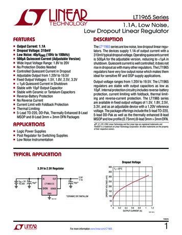
BlueNRG-2NHigh performance and benefits1High performance and benefitsThe BlueNRG-2N shows a reliable communication thanks to the best-in-class output power level assuring arobust communication even in a noisy corrupted scenario without compromising the overall power consumption.The BLUENRG-2N collaterals include comprehensive tools for developers such as a full featured SDK including: Templates High-level abstraction layer APIs (no BLE expertise required) Real-time debug capabilitiesA dedicated firmware is provided to support the interface with an external application processor. The wholeBluetooth low energy stack runs in the BlueNRG-2N; the GATT profiles are provided to run in the applicationprocessor together with the application code. The figure below shows the network processor RF software layers.Figure 1. BlueNRG-2N network processor RF software layersDS13280 - Rev 3page 3/47
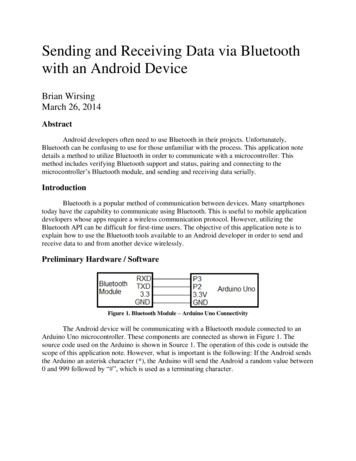
BlueNRG-2NFunctional details2Functional detailsThe BlueNRG-2N integrates: ARM Cortex-M0 corePower management Clocks Bluetooth low energy radio Random number generator (RNG) (reserved for Bluetooth low energy protocol stack, but user applicationscan read it) External microcontroller interface (SPI/UART) Public key cryptography (PKA) (reserved for Bluetooth low energy protocol stack)2.1CoreThe ARM Cortex -M0 processor has been developed to provide a low-cost platform that meets the needsof MCU implementation, with a reduced pin count and low-power consumption, while delivering outstandingcomputational performance and an advanced system response to interrupts.The ARM Cortex -M0 32-bit RISC processor features exceptional code-efficiency, delivering the highperformance expected from an ARM core in the memory size usually associated with 8-bit and 16-bit devices.The BlueNRG-2N has an embedded ARM core and is therefore compatible with all ARM tools and software.The ARM Cortex M0 processor is reserved for internal operations and it is not open to customer applicationdevelopments.2.2Power managementThe BlueNRG-2N integrates both a low dropout voltage regulator (LDO) and a step-down DC-DC converter tosupply the internal BlueNRG-2N circuitry.The BlueNRG-2N most efficient power management configuration is with DC-DC converter active where bestpower consumption is obtained without compromising performances. Nevertheless, a configuration based on LDOcan also be used, if needed.A simplified version of the state machine is shown below.Figure 2. BlueNRG-2N power management state machineDS13280 - Rev 3page 4/47
BlueNRG-2NClocks and reset management2.2.1State description2.2.1.1Preactive stateThe preactive state is the default state after a POR event.In this state: All the digital power supplies are stable.The high frequency clock runs on internal fast clock RC oscillator (16 MHz). The low frequency clock runs on internal RC oscillator (32.768 kHz).2.2.1.2Active stateIn this state: The high frequency runs on the accurate clock (32 MHz 50 ppm) provided by the external XO. The internalfast clock RO oscillator is switched off.2.2.1.3Standby stateIn this state: Only the digital power supplies necessary to keep the RAM in retention are used.2.2.1.4Sleep stateIn this state: Only the digital power supplies necessary to keep the RAM in retention are used The low frequency oscillator is switched onThe wake-up from this low power state is driven by the following sources: Internal timers SPI CS (SPI mode only)2.2.1.5Power saving strategyThe application power saving strategy is based on clock stopping, dynamic clock gating,digital power supply switch-off and analog current consumption minimization.A summary of functional blocks versus the BlueNRG-2N states is provided below.Table 1. Relationship between the BlueNRG-2N states and functional blocksFunctional blocksRESETSTANDBYSLEEPPreactiveActiveLOCK RX/LOCK TXRXTXLDO SOFT 1V2 orLDO SOFT 0V9OFFONONONONONONONLDO STRONG 1V2OFFOFFOFFONONONONONLDO DIG 1V8OFFOFFOFFONONONONONSMPSOFFOFFOFFONONONONONLDO DIG 1V2OFFOFFOFFONONONONONBOROFFOFFOFFONONONONON16 MHz ROOFFOFFOFFONOFFOFFOFFOFF32 MHz XOOFFOFFOFFOFFONONONON32 kHz RO or XOOFFOFFONONONONONON2.3Clocks and reset managementThe BlueNRG-2N embeds an RC low-speed frequency oscillator at 32 kHz and an RO high-speed frequencyoscillator at 16 MHz.DS13280 - Rev 3page 5/47
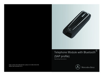
BlueNRG-2NClocks and reset managementThe low-frequency clock is used in low power mode and can be supplied either by a 32.7 kHz oscillator that usesan external crystal and guarantees up to 50 ppm frequency tolerance, or by a ring oscillator, which does notrequire any external components.The primary high-speed frequency clock is a 32 MHz crystal oscillator. A fast-starting 16 MHz ring oscillatorprovides the clock while the crystal oscillator is starting up. Frequency tolerance of the high-speed crystaloscillator is 50 ppm.Usage of the high-speed crystal usage is strictly necessary for RF communications.2.3.1Reset managementFigure 3. Reset and wake-up generation shows the general principle of reset. Releasing the reset pin takesthe chip out of shutdown state. The wake-up logic is powered and receives the POR. Each time the wake-upcontroller decides to exit sleep or standby modes, it generates a reset for the core logic. The core logic can alsobe reset by: Watchdog Reset request from the processor (system reset) LOCKUP state of the Cortex-M0The SWD logic is reset by the POR. It is important to highlight that the reset pin actually powers down the chip, soit is not possible to perform debug access with system under reset.Figure 3. Reset and wake-up generationIf, for any reason, the user would like to power off the device there are two options:1.Force RESETN pin to ground, keeping VBAT level2.To put VBAT pins to ground (e.g. via a transistor)In the second option, care must be taken to ensure that no voltage is applied to any of the other pins as thedevice can be powered and have an anomalous power consumption. The ST recommendation is to use RESETNwhenever it is possible.2.3.1.1Power-on-ResetThe Power-on-Reset (POR) signal is the combination of the POR signal and the BOR signal generated by theanalog circuitry contained in the BlueNRG-2N device. The combination of these signals is used to generate theinput to the Cortex-M0, which is used to reset the debug access port (DAP) of the processor. It is also used togenerate the signal, which resets the debug logic of the Cortex-M0. The POR signal also resets the TAP controllerof the BlueNRG-2N and a part of the Flash controller (managing the Flash memory boot, which does not need tobe impacted by system resets).The BOR reset is enabled by default. At software level, it can be decided to change the default values after reset.2.3.1.2Power-up sequenceThe starting sequence of the BlueNRG-2N supply and reset signal is shown below.DS13280 - Rev 3page 6/47
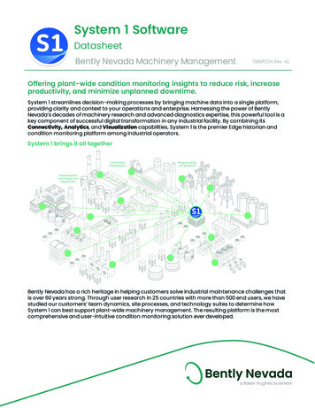
BlueNRG-2NClocks and reset managementFigure 4. BlueNRG-2N power-up sequenceVBATxX 1,2,330 µsRESETN1.82 ms max.Internal PORSystem clockCPU activity Note:CPU under resetCPU is running onRCO 16 MHzCPU can switch onXO 32 MHz by SWThe VBATx power must only be raised when RESETN pin is low.The different VBATx (x 1,2,3) power can be raised separately or together.Once the VBATx (x 1,2,3) reaches the nominal value, the RESETN pin could be driven high after a 30 us.The internal POR is released once internal LDOs are established and RCO clock is ready.The system starts on RCO 16 MHz clock system. The software is responsible for configuring the XO 32 MHzwhen necessary.The minimum negative pulse to reset the system must be at least 30 µs.The POR circuit is powered by a 1.2 V regulator, which must also be powered up with the correct startupsequence. Before VBAT has reached the nominal value, RESETN line must be kept low. An external RC circuiton RESETN pin adds a delay that can prevent RESETN signal from going high before VBAT has reached thenominal value.Figure 5. Reset circuitDS13280 - Rev 3page 7/47
BlueNRG-2NTX/RX event alertIf the above conditions are not satisfied, ST cannot guarantee the correct operation of the device.The BlueNRG-2N could inform the external microcontroller via the host interface protocol on the internal resetreason, which includes: POR, BOR, watchdog, lockup.2.4TX/RX event alertThe BlueNRG-2N is provided with the ANATEST1 (pin 14 for QFN32 package, pin D4 for WCSP34 package)signal which alerts forthcoming transmission or reception event. The ANATEST1 pin switches to high level about18 μs before transmission before reception. Then, it switches to low level at the end of the event. The signal canbe used for controlling external antenna switching and supporting coexistence with other wireless technologies.2.5SWD debug featureThe BlueNRG-2N embeds the ARM serial wire debug (SWD) port. It is two pins (clock and single bi-directionaldata) debug interface, providing all the debug functionality plus real-time access to system memory withouthalting the processor or requiring any target resident code.The SWD interface is provided to allow firmware upgrade on the device in the production lines.Table 2. SWD portPin functionalityPin namePin descriptionSWCLKIO9SWD clock signalSWDIOIO10SWD data signalThe Cortex-M0 subsystem of the BlueNRG-2N embeds four breakpoints and two watchpoints.2.6Bluetooth low energy radioThe BlueNRG-2N integrates an RF transceiver compliant to the Bluetooth specification and to the standardnational regulations in the unlicensed 2.4 GHz ISM band.The RF transceiver requires very few external discrete components. It provides 96 dB link budgets with excellentlink reliability, keeping the maximum peak current below 15 mA.In transmit mode, the power amplifier (PA) drives the signal generated by the frequency synthesizer out to theantenna terminal through a very simple external network. The power delivered as well as the harmonic contentdepends on the external impedance seen by the PA.2.6.1Radio operating modesSeveral operating modes are defined for the BlueNRG-2N radio: Reset modeSleep mode Active mode Radio mode–RX mode–TX modeIn Reset mode, the BlueNRG-2N is in ultra-low power consumption: all voltage regulators, clocks and the RFinterface are not powered. The BlueNRG-2N enters Reset mode by asserting the external Reset signal. As soonas it is de-asserted, the device follows the normal activation sequence to transit to active mode.In sleep mode either the low speed crystal oscillator or the low speed ring oscillator are running, whereas the highspeed oscillators are powered down as well as the RF interface. The state of the BlueNRG-2N is retained and thecontent of the RAM is preserved.While in sleep mode, the BlueNRG-2N waits until an internal timer expires and then it goes into active mode.In active mode the BlueNRG-2N is fully operational: all interfaces, including RF, are active as well as all internalpower supplies together with the high speed frequency oscillator. The MCU core is also running.DS13280 - Rev 3page 8/47
BlueNRG-2NFirmware imageRadio mode differs from active mode as the RF transceiver is also active and is capable of either transmitting orreceiving.2.7Firmware imageThe Bluetooth Low Energy stack runs on the embedded ARM Cortex-M0 core. The stack is stored on theon-chip non-volatile Flash memory at a specific offset (0x2000) and can be easily upgraded through a dedicatedpre-programmed device updater FW stored at device Flash base address, and using the selected hardwareinterface to external microcontroller. If DIO3 is high at power-up or hardware reset the device updater FW isactivated.The device comes pre-programmed with a production-ready stack image (version may
2.2 Power management. The BlueNRG-2N integrates both a low dropout voltage regulator (LDO) and a step-down DC-DC converter to supply the internal BlueNRG-2N circuitry. The BlueNRG-2N most efficient power management configuration is with DC-DC converter active where best power consumption is obtained without compromising performances. Nevertheless, a configuration based on LDO