Transcription
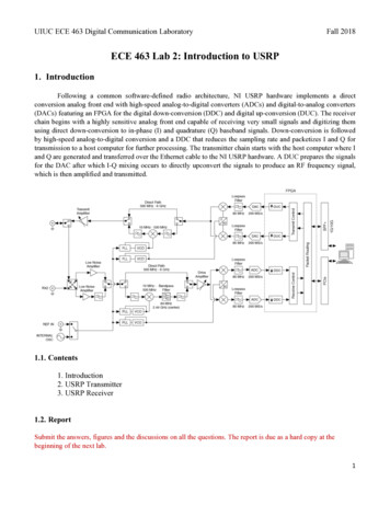
UIUC ECE 463 Digital Communication LaboratoryFall 2018ECE 463 Lab 2: Introduction to USRP1. IntroductionFollowing a common software-defined radio architecture, NI USRP hardware implements a directconversion analog front end with high-speed analog-to-digital converters (ADCs) and digital-to-analog converters(DACs) featuring an FPGA for the digital down-conversion (DDC) and digital up-conversion (DUC). The receiverchain begins with a highly sensitive analog front end capable of receiving very small signals and digitizing themusing direct down-conversion to in-phase (I) and quadrature (Q) baseband signals. Down-conversion is followedby high-speed analog-to-digital conversion and a DDC that reduces the sampling rate and packetizes I and Q fortransmission to a host computer for further processing. The transmitter chain starts with the host computer where Iand Q are generated and transferred over the Ethernet cable to the NI USRP hardware. A DUC prepares the signalsfor the DAC after which I-Q mixing occurs to directly upconvert the signals to produce an RF frequency signal,which is then amplified and transmitted.1.1. Contents1. Introduction2. USRP Transmitter3. USRP Receiver1.2. ReportSubmit the answers, figures and the discussions on all the questions. The report is due as a hard copy at thebeginning of the next lab.1
UIUC ECE 463 Digital Communication LaboratoryFall 20182. USRP Transmitter2.1. Transmitter OverviewLabVIEW can interact with the USRP transmitter by the blocks under Hardware Interfaces NI-USRP Tx. Thefollowing diagram shows the basic setup for the USRP transmitter. We will start by building the below diagramand add/modify more functions/algorithms in the rest lab sessions.The diagram has the following main components: Open Tx Session: Opens a transmit (Tx) session to thedevice you specify in the device names input and returnssession handle as output. You must add a control called“device names” that you will use to inform LabVIEW ofthe IP address or resource name of the USRP. Configure Signal: Configures parameters of Tx or Rx. IQrate is the sampling rate of the baseband I/Q data insamples per second (S/s). Carrier frequency is the carrierfrequency of the RF signal in Hz. Gain is the Tx gainapplied to the RF signal in dB. Active antenna is theantenna port to use for this channel. Coerced IQrate/carrier frequency/gain are the actual corresponding values supported by the device. Write Tx data: writes complex, 16-bit signed integerdata to the specified channel. The baseband samples totransmit as an array of complex, 16-bit signed integerdata. The real and imaginary components of the datacorrespond to the in-phase (I) and quadrature-phase (Q)data, respectively. I and Q are interleaved [I, Q, I, Q, .]in the array. Close Session: Closes the session handle to the device.2
UIUC ECE 463 Digital Communication LaboratoryFall 20182.2. Construct the USRP TransmitterStart by building the above diagram. In this section, we will simply transmit the carrier frequency without any IQsignal modulation.1. Make sure the USRP is connected to the machine and turned on.2. Run the NI-USRP Configuration Utility software by clicking Windows Start National InstrumentsFolder NI-USRP Configuration Utility.3. Find the device ID and the connection type. The USRP device is not hot-pluggable over PCI express. TheUSRP SHOULD be power-on prior to your computer.4. Open a blank VI and rename as “carrier.gvi”.5. Place Open Tx Session, Configure Signal, Write Tx Data, and Close Session.6. Click Open Tx Session and find “Create Constant” button in the item panel in the right side. Input yourUSRP device ID in the constant box.7. Create a “cluster properties” block. In Behavior tab, set all to write.8. Wire the session handle ports through all four USRP blocks (Open Tx Session Cluster Properties Configure Signal Write Tx Data Close Session).9. Click the cluster properties block, and select Configuration Enabled Channels. Left-click the port andcreate a constant. Input “0” for the enabled channel. This will enable “RF0” channel in the front panel ofthe USRP.10. Create three DBL-type controls: IQ rate, Carrier Frequency, and Gain. Create a string-type control,Active Antenna. Create three DBL-type indicators: Coerced IQ rate, Coerced Carrier Frequency, andCoerced Gain. Connect the controls and the indicators to the corresponding ports of the Configure Signal.11. Create a while loop and place the Write Tx Data block inside.12. Wire the Error out ports through all four USRP blocks. Create an Error indicator and wire the Error outport of Close Session.13. Create a Stop button and place it inside the loop. Use OR block to take the stop signal and the error outfrom the Write Tx Data block. Feed the output of OR block to the terminal condition.14. The diagram will look like the following figure. Save the current vi and duplicate it. Rename the new vias “tx template.gvi”. We will re-use the vi in the next following labs, so keep it. Go back to “carrier.gvi”.3
UIUC ECE 463 Digital Communication LaboratoryFall 201815. As described in the introduction, the USRP Tx/Rx is a quadrature modulation system. It mixes the inphase (I) signal with the cosine wave (whose frequency is the “carrier frequency”) and the quadraturephase (Q) signal with the sine wave. The Write Tx Data block takes the IQ baseband-samples andmodulates them with the two sinusoids. Note that the input data of the Write Tx Data block can havevarious different types. We’ll use the complex double (CDB) array. Click the block and change the functionconfiguration to Write Tx Data (CDB). The real and imaginary parts of this complex data arraycorrespond to the in-phase (I) and quadrature-phase (Q) data, respectively.16. We will now generate a single sinusoid signal at the carrier frequency. To do that, we will input a constantnumber of array for the baseband-samples. Use “Initialize Array” block. The diagram will look like as thefollowing figure.17. Set the parameters as follows:o IQ rate 1Mo Carrier frequency 2Go Gain 0o Active antenna TX1o Waveform size 100018. Connect the TX1 output port to the spectrum analyzer using SMA cables and a 20dB attenuator. Verifythat a right signal is generated.19. Change the carrier frequency to 1G, 2.5G, 3G, 4G, 5G, and verify that you see the correct frequency onthe spectrum analyzer.4
UIUC ECE 463 Digital Communication LaboratoryFall 20182.3. Transmitting Sinusoidal SignalWe will now generate a sinusoidal signal with a frequency offset to the carrier frequency and transmit it. Instead ofthe constant data, we will feed a cosine waveform to in-phase data and a sine waveform to quadrature-phase data.1. Duplicate the VI and rename as “upper-side IQ.gvi”. Remove the Initialize Array, its numeric constantand the wire to the Write Tx Data.2. Create two more double-type controls: Tone frequency and Tone amplitude.3. Place two “Wave Generator” blocks from Analysis Signal Processing Generation. By default, the blockis “Sine” wave and “Waveform” data type.4. Wire the Tone frequency control to the Frequency port of the two Wave Generator blocks and the Toneamplitude control to the Amplitude port. Wire the Waveform size control to the Samples port. Wire theSample rate port to the Coerced IQ rate indicator.5. Create a numeric constant of “90” and wire it to the “Phase in” port of one of the Wave Generator blocks.6. Use “Waveform Properties” to get the cosine and sine samples from the Wave Generator blocks.7. Use “Real and Imaginary to Complex” to receive the cosine and sine samples and convert them to complexnumbers. You should get the below diagram.8. Set the parameters as follows:o IQ rate 1Mo Carrier frequency 2Go Gain 0o Active antenna TX1o Waveform size 1000o Tone frequency 1ko Tone amplitude 19. Connect the TX1 output port to the spectrum analyzer using SMA cables and a 20dB attenuator. Verifythat a right signal is generated.10. Change the tone frequency to 10k, 50k, 100k, and verify that the correct tone appears on the spectrumanalyzer.5
UIUC ECE 463 Digital Communication LaboratoryFall 20182.4. Questions2.4.1. Compare the results from “carrier.gvi” and “upper-side IQ.gvi”. Include the spectrum of eachcase in the report. What differences can you see?2.4.2. Change the waveform size to 1005 and measure the spectrum. What result do you get?2.4.3. Create “lower-side IQ.gvi” which implements a similar code to “upper-side IQ.gvi” but themain tone is located lower than the carrier frequency tone.2.4.4. Create “double-side IQ.gvi” which implements a similar code to “upper-side IQ.gvi” but withtwo tones that are located on both the upper and lower side of the carrier frequency tone. Howdoes the amplitude of the tone differ in each case?2.4.5. Derive the mathematical equations that show why in each case we get a upper-side, lower-side ordouble-side tones.6
UIUC ECE 463 Digital Communication LaboratoryFall 20183. USRP Receiver3.1. Receiver OverviewLabVIEW can interact with the USRP receiver by the blocks under Hardware Interfaces NI-USRP Rx. Thefollowing diagram shows the basic setup for the USRP receiver. We will start from this diagram and add/modifymore functions/algorithms in the rest lab sessions. Open Rx Session: Opens a reciver (Rx) session to thedevice you specify in the device names input and returnssession handle out. You must add a control called “devicenames” that you will use to inform LabVIEW of the IPaddress or resource name of the USRP. Initiate: Starts the Rx acquisition. Fetch Rx Data: Fetches complex, 16-bit signed integerdata from the specified channel. Number of samplesdefined the samples to fetch from the acquisition channel.Data is the received baseband samples as an array ofcomplex, 16-bit signed integer data. The real and imaginarycomponents of the data correspond to the in-phase (I) andquadrature-phase (Q) data, respectively. I and Q are interleaved [I, Q, I, Q, .] in the array. The total numberof elements returned in the array equals the value of the number of samples parameter x 2. Abort: Stops an acquisition previously started.7
UIUC ECE 463 Digital Communication LaboratoryFall 20183.2. Construct the USRP ReceiverWe will start by building the above receiver diagram.1. Open a blank VI and rename as “Rx.gvi”.20. Place Open Rx Session, Configure Signal, Initiate, Fetch Rx Data, Abort and Close Session. Similarto Tx, create the controls and indicators for IQ rate, carrier frequency, gain, and active antenna. Input “1”for the enabled channel. This will enable “RF1” channel in the front panel of the USRP. Create a whileloop for Fetch Rx Data. Click the Fetch Rx Data. Change its Function Configuration to Fetch Rx Data(CDB WDT). The diagram will look like as the following figure. Rename the new vi as “rx template.gvi”.We will re-use the vi in the next following labs, so keep it. Go back to “Rx.gvi”.2. In Rx, we want to display the spectrum of the received signal just like the spectrum analyzer. We also wantto display the in-phase signal and the quadrature-phase signal in the time domain.3. Place “FFT Power Spectrum and PSD” block from Analysis Signal Processing Measurement. Changeits Function Configurations to “Power Spectrum” and “Continuous”. Check “dB on” to display in dB scale.Wire the data port of Fetch Rx Data to the signal port. To display the spectrum, go to the panel and createGraph from “Graphs and Charts”. Go back to the diagram and connect the graph indicator to the powerspectrum port.4. Create Waveform Properties for the data port of Fetch Rx Data. Use “Complex to Real and Imaginary”to extract I and Q samples from the complex array. Use Build Waveform blocks and Waveform indicatorsto display the IQ time domain samples.8
UIUC ECE 463 Digital Communication LaboratoryFall 20185. Set the parameters as follows:o IQ rate 1Mo Carrier frequency 2Go Gain 0o Active antenna RX2o Number of samples 1006. Connect the TX1 antenna port of RF0 to the RX2 antenna port of RF1 using an SMA cable and a 30 dBattenuator and run the code.3.3. Questions3.3.1. While running “upper-side IQ.gvi”, run “Rx.gvi” and measure the signal. Compare the resultwith the spectrum analyzer. You can pick one tone-frequency for Tx (Hint: For more stablemeasurement, you can use “average parameter” in the power spectrum block).3.3.2. Repeat the analysis with “lower-side IQ.gvi” and “double-side IQ.gvi”.3.3.3. Change the sine wave signal in above 3 examples to a square wave. How does the spectrumdiffer in each case?3.3.4. Use the mathematical results derived in 2.4.5. and derive the equations for the down-convertedsignals in each case.3.3.5. Connect Rx2 to a 2.4/5 GHz antenna. Your goal is to capture WiFi signals (or Bluetooth). Turn onWiFi on your smartphone and place it next to the receiver antenna. Run a high data rate applicationsuch as Youtube or Netflix. WiFi has many channels but some of the most common ones used byIllinoisNet are centered at 2.414 GHz, 2.437 GHz, 2.462 GHz, 5.22 GHz, 5.26 GHz, 5.5 GHz, 5.58GHz, 5.62 GHz, 5.765 GHz, 5.785 GHz, . Change the carrier frequency until you start to seesignals on the LabVIEW spectrum analyzer you built. Show the result you get. (Hint: You can firstuse the spectrum analyzer to locate the carrier frequency. Use “Max hold” in “Trace” menu tohold the peak.)3.3.6. WiFi signals can have a bandwidth of 20 MHz to 40 MHz. Increase the IQ rate so you can capturethe full signal. Show the result you get.3.3.7. Save all the VIs and the Project since they will be used in subsequent labs.9
2. USRP Transmitter 2.1. Transmitter Overview LabVIEW can interact with the USRP transmitter by the blocks under Hardware Interfaces NI-USRP Tx. The following diagram shows the basic setup for the USRP transmitter. We will start by building the below diagram and add/modify more functions/algorithms in the rest lab sessions.