Transcription
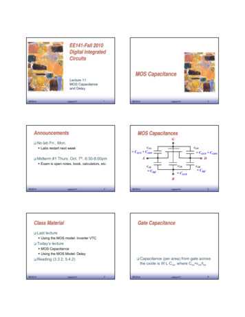
EE141-Fall 2010Digital IntegratedCircuitsMOS CapacitanceLecture 11MOS Capacitanceand DelayEE141EECS141Lecture #1111Announcements NoEE141EECS1414MOS CapacitancesGlab Fri., Mon. Labs restart next week Midterm4Lecture #11CGSCGD CGCS CGSO#1 Thurs. Oct. 7th, 6:30-8:00pm CGCD CGDOS Exam is open notes, book, calculators, etc.DCGBCSB Cdiff CGCBCDB CdiffBEE141EECS141Lecture #1122Class Material LastEE141EECS141Lecture #1155Gate Capacitancelecture Using the MOS model: Inverter VTC Today’slecture MOS Capacitance Using the MOS Model: Delay ReadingEE141EECS141 Capacitance(per area) from gate acrossthe oxide is W·L·Cox, where Cox εox/tox(3.3.2, 5.4.2)Lecture #1133EE141EECS141Lecture #1166
Gate CapacitanceTransistor in Linear RegionGSDWLC OLC jSB Distributionbetween terminals is complex Capacitance is really distributed Several operating regions:– Way off, off, transistor linear, transistor saturated7Lecture #117Transistor In Cutoff Channel is formed and acts as the other terminal Model by splitting oxide cap equally betweensource and drain– Changing either voltage changes the channel chargeEE141EECS141GSLC OLxjC jDB– Substrate acts as the other capacitor terminal– Capacitance becomes series combination of gateoxide and depletion capacitance8Lecture #11 Changing source voltage doesn’t change VGCuniformlyEE141EECS141Transistor in Saturation Region (cont’(cont’d)GSDWLC OLC OLxjC jDB99C OLxjC jDBLD Drain voltage no longer affects channel charge– Set by source and VDS sat– Usually just approximate with CGCB 0 in this region. (If VGS is “very” negative (for NMOS), depletionregion shrinks and CGCB goes back to W·L·Cox)CGC JCC jSB When VGS VT , total CGCB much smaller thanW·L·CoxLecture #111111Lecture #11LEE141EECS141C jDBLDDWC jSBxj Bottom line: CGCS 2/3·W·L·Cox8GC GBC OL– E.g. VGC at pinch off point still VTHTransistor In Cutoff (cont’(cont’d)C OLCGC JCC jSB When the transistor is off, no carriers in channelto form the other side of the capacitor.SDWLC OLC jSBEE141EECS1411010Lecture #11DC GBC jDBTransistor in Saturation RegionWC OLxjLDGSC OL– CGCB drops to zero (shielded by channel)– Useful models lump it to the terminalsEE141EECS141CGC JC If change in charge is 0, CGCD 0EE141EECS141Lecture #111212
Diffusion CapacitanceGate CapacitanceNA BottomSide wall– Area cap– Cbottom Cj·LS·WSourceWNDBottom SidewallsxjSide wall– Perimeter cap– Csw Cjsw·(2LS W)Cgate vs. VGS(with VDS 0)Cgate vs. operating regionChannelSubstrateLSNA GateEdge– Cge Cjgate·W– Usually automatically included in the SPICE modelEE141EECS1411313Lecture #11Gate Overlap Capacitance1.0SourcetoxDrainxdn WGate-bulkoverlapLdLn n Top view Junction capsare nonlinear– CJ is afunction ofjunction biasCross section0.9Capacitance [arbitrary units]Gate oxidexd1616Lecture #11Junction Capacitance (2)Polysilicon gaten EE141EECS1410.80.70.6N junction areaN junction perimeterP junction areaP junction perimeter0.5 SPICE modelequations:CO Cox xd0.40.00.20.40.60.81.01.21.41.6Node voltage (V))mj– Area CJ area CJ0 / (1 VDB /φΒ– Perimeter CJ perim CJSW / (1 VDB /φΒ)mjsw– Gate edge CJ W CJgate / (1 VDB /φΒ)mjswgOff/Lin/Sat Æ CGSO CGDO CO·W How do we deal with nonlinear capacitance?EE141EECS1411414Lecture #11Gate Fringe CapacitanceLecture #111717Linearizing the Junction CapacitanceFringing fieldsn EE141EECS141Replace non-linear capacitance bylarge-signal equivalent linear capacitancewhich displaces equal charge over voltage swing of interestn Cross section COV not just from metallurgic overlap – get fringingfields too Typical value: 0.2fF·W(in µm)/edgeEE141EECS141Lecture #111515EE141EECS141Lecture #1118181.8
Capacitance Model Summary Model Calibration - CapacitanceGate-Channel Capacitance CGC 0 CGC Cox·W·Leff( VGS VT )(Linear) Can calculate Cg, Cd based on tech. parameters CGC (2/3)·Cox·W·Leff(Saturation) Another approach:– But these models are simplified too– 50% G to S, 50% G to D– Tune (e.g., in spice) the linear capacitance until itmakes the simplified circuit match the real circuit– Matching could be for delay, power, etc.– 100% G to S Gate Overlap Capacitance CGSO CGDO CO·W (Always)CloadJunction/Diffusion Capacitance Cdiff Cj·LS·W Cjsw·(2LS W) re #11Capacitances in 0.25 µm CMOSProcessEE141EECS1412222Lecture #11Model Calibration for DelayACloadDelay1Delay2Match For gate capacitance:– Make inverter fanout 4– Adjust Cload until Delay1 Delay2 For diffusion capacitance– Replace inverter “A” with a diffusion capacitance loadEE141EECS1412020Lecture #11Simplified ModelEE141EECS1412323Lecture #11Delay Calibration Capacitance models important for analysisand intuition141664Load?– But often need something simpler to work with Simple switch model:Delay– Lump together as effective linear capacitance to(ac) ground– In most processes: CG CD 1.5 – 2fF·W(µm)VinVoutVin"Edge Shaper" Why did we need that last inverter stage?VoutCLEE141EECS141Lecture #112121EE141EECS141Lecture #112424
The Miller EffectMOS Transistor as a Switch As Vin increases, Vout drops– Once get into the transition region, gainfrom Vin to Vout 1Cgd1 Vthat real transistors aren’t exactlyresistors VVin So, Cgd experiences voltage swinglarger than Vin SawVout Look more like current sources in saturationM1– Which means you need to provide morecharge– Makes Cgd look larger than it really is Two Known as the “Miller Effect” in theanalog worldEE141EECS141questions: Which region of IV curve determines delay? How can that match up with the RC model?2525Lecture #11EE141EECS1412828Lecture #11Transistor Driving a Capacitor With a step input:VGS VDDIDVDD Æ VDD/2CMOSSwitching DelayVDSVVSAT VDD /2VDD Transistor is in (velocity) saturation during entire transitionfrom VDD to VDD/2EE141EECS1412626Lecture #11MOS Transistor as a Switch In saturation, transistor basically acts like a current source:VOUTVOUTVDDi D i D (v DS )iD CdVDSdtIDSATCVDD/2 We modeled this with:ttpRVOUT VDD - (IDSAT/C)ttp ln (2) RCCEE141EECS1412929Lecture #11Switching Delay Discharging a capacitorCEE141EECS141Lecture #112727EE141EECS141tp C(VDD/2)/IDSATLecture #113030
Switching Delay (with Output Conductance)The Book’s Method Including output conductance:VOUTIDSATC1/(λIDSAT)VOUT (VDD λ 1 ) e For “small” λ:tp -t ( C λI DSAT )- λ 1C (VDD 2 )(1 λVDD ) I DSATEE141EECS1413131Lecture #11RC ModelEE141EECS1413434Lecture #11The Transistor as a Switch Transistor current not linear on VOUT – how is the RCmodel going to work?7x 1056 Look at waveforms:2.55 Voltage looks like aramp for RC τEE141EECS141321.504eqNMOS1.7ROUT1.93232Lecture #11DD22.5(V)1Finding ReqEE141EECS141Lecture #113535The Transistor as a Switch Match the delay of the RC model with the actual delay:tp t p , RCC (VDD 2 ) ln ( 2 ) Req C(1 λVDD ) I DSAT Often just:Req Req (VDD 2 )ln ( 2 )(1 λVDD ) I DSAT1VDD2 ln ( 2 ) I DSAT Note that the book uses a different method and gets0.75·VDD/IDSAT instead of 0.72·VDD/IDSAT. Why did we do it this way vs. the book’s method?EE141EECS141Lecture #113333EE141EECS141Lecture #113636
d based on tech. parameters -But these models are simplified too Another approach: -Tune (e.g., in spice) the linear capacitance until it makes the simplified circuit match the real circuit -Matching could be for delay, power, etc. Cload Delay1 Match Delay2 EE141 23 EECS141 Lecture #11 23 Model Calibration for Delay For gate capacitance: