Transcription
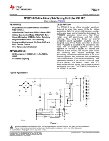
TPS92310www.ti.comSNVS792 – FEBRUARY 2012TPS92310 Off-Line Primary Side Sensing Controller With PFCCheck for Samples: TPS92310FEATURESDESCRIPTION The TPS92310 is an off-line controller specificallydesigned to drive high power LEDs for lightingapplications. With the primary side sensing, constanton-time and quasi-resonant switching techniques, theTPS92310 application circuit gives high PowerFactor, good EMI performance and high systemefficiency. Also, using this device, low externalcomponent count application solutions can bedesigned easily. Power Factor Correction is inherentif the TPS92310 is operated in the constant on-timemode with an adaptive algorithm. The controlalgorithm of TPS92310 adjusts the on-time withreference to the primary side inductor peak currentand secondary side inductor discharge timedynamically, the response time of which is set by anexternal capacitor. Also, minimized EMI and switchingloss is achieved with quasi-resonant switching. Othersupervisory features of the TPS92310 include cycleby-cycle primary side inductor current limit, VCCunder-voltage lockout, output over-voltage protectionand thermal shutdown. The TPS92310 is available inthe VSSOP-10 package.12 Regulates LED Current Without SecondarySide SensingAdaptive ON-Time Control With Inherent PFCCritical-Conduction-Mode (CRM) With ZeroCurrent Detection (ZCD) for Valley SwitchingProgrammable Switch Turn ON DelayProgrammable Constant ON-Time (COT) andPeak Current ControlOver-Temperature ProtectionAPPLICATIONS LED Lamps: A19 (E26/27, E14), PAR30/38,GU10Solid State LightingTypical ApplicationD3T1CIND1LED DE1DLYMODE2Q1RISNSRDLY*OptionalFigure 1.12Please be aware that an important notice concerning availability, standard warranty, and use in critical applications ofTexas Instruments semiconductor products and disclaimers thereto appears at the end of this data sheet.All trademarks are the property of their respective owners.PRODUCTION DATA information is current as of publication date.Products conform to specifications per the terms of the TexasInstruments standard warranty. Production processing does notnecessarily include testing of all parameters.Copyright 2012, Texas Instruments Incorporated
TPS92310SNVS792 – FEBRUARY 2012www.ti.comConnection DiagramTop ViewVCCGATEZCDISNSAGNDPGNDCOMPMODE1DLYMODE2Figure 2. 10-Pin VSSOPPin Descriptions2PinNameDescription1VCCPower supply inputApplication Information2ZCDZero crossing detection input3AGNDSmall signal ground4COMPCompensation networkOutput of the error amplifier. Connect a capacitor from this pin toground to set the frequency response of the LED current regulationloop.5DLYDelay control inputConnect a resistor from this pin to ground to set the delay betweenswitching ON and OFF periods.6MODE2Mode selection input 2Select operating mode for isolated or non-isolated mode.7MODE1Mode selection input 1Select operating mode for peak current mode or constant ON time.8PGNDPower ground9ISNSCurrent sense voltage feedback10GATEGate driver outputThis pin provides power to the internal control circuitry and gate driver.Connect a 10µF capacitor from this pin to ground.The pin senses the voltage of the auxiliary winding for zero currentdetection.Signal ground.Power ground. This pin must be connected to the AGND pin externallyfor normal operation. This pin has no internal connection to PGND.Switch current sensing input.Gate driving signal to the external switching MOSFET.Submit Documentation FeedbackCopyright 2012, Texas Instruments IncorporatedProduct Folder Links: TPS92310
TPS92310www.ti.comSNVS792 – FEBRUARY 2012These devices have limited built-in ESD protection. The leads should be shorted together or the device placed in conductive foamduring storage or handling to prevent electrostatic damage to the MOS gates.Absolute Maximum Ratings (1) (2)VCC to GND-0.3V to 40VDLY, COMP, ZCD to GND-0.3V to 7VISNS to GND-0.3V to 7VGATE to GND-0.3V to 12V (5ns, –5V)MODE1 to GND-0.3V to 7VMODE2 to GNDESD Rating, HBM-0.3V to 7V(3) 2 kVMachine Model200VStorage Temperature Range-65 C to 125 CJunction Temperature(1)(2)(3) 150 CAbsolute maximum ratings are limits beyond which damage to the device may occur. Operating Ratings are conditions for which thedevice is intended to be functional, but device parameter specifications may not be ensured. For ensured specifications and testconditions, see the Electrical Characteristics. All voltages are with respect to the potential at the GND pin, unless otherwise specified.If Military/Aerospace specified devices are required, please contact the Texas Instruments Sales Office/Distributors for availability andspecifications.Human Body Model, applicable std. JESD22-A114-C.Operating ConditionsSupply Voltage range VCC13V to 36VJunction Temperature (TJ)Thermal Resistance (θJA)(1)-40 C to 125 C(1)120 C/WJunction-to-ambient thermal resistance is highly application and board-layout dependent. In applications where high maximum powerdissipation exists, special care must be paid to thermal dissipation issues in board design. In applications where high power dissipationand/or poor package thermal resistance is present, the maximum ambient temperature may have to be derated. Maximum ambienttemperature (TA-MAX) is dependent on the maximum operating junction temperature (TJ-MAX-OP 125 C), the maximum power dissipationof the device in the application (PD-MAX), and the junction-to ambient thermal resistance of the part/package in the application (RθJA), asgiven by the following equation: TA-MAX TJ-MAX-OP – (RθJA PD-MAX).Electrical CharacteristicsVCC 18V unless otherwise indicated. Typicals and limits appearing in plain type apply for TA TJ 25 C. Limits appearingin boldface type apply over the full Operating Temperature Range. Data sheet minimum and maximum specification limitsare specified by design, test or statistical C Turn on threshold23.4 / 23VCCTurn off threshold11.1 / 10.425.627.8 / 29V1314.7 / 15.7VSUPPLY VOLTAGE INPUT (VCC)VCC-UVLOHysteresis12.6ISTARTUPStartup CurrentVCC VCC-UVLO–3.0V1012.514.75µAIVCCOperating supply currentNot switching0.91.21.5mA65kHz switching, CLOAD 1nF2mAZERO CROSS DETECT (ZCD)IZCDZCD bias currentVZCD-OVPZCD over-voltagethresholdVZCD 5VTOVPOver voltage de-bouncetimeVZCD-ARMZCD Arming thresholdVZCD Increasing1.16VZCD-TRIGZCD Trigger thresholdVZCD Decreasing0.48VZCD-HYSZCD e1.241.3V0.60.77V0.64Submit Documentation FeedbackCopyright 2012, Texas Instruments IncorporatedProduct Folder Links: TPS92310V3
TPS92310SNVS792 – FEBRUARY 2012www.ti.comElectrical Characteristics (continued)VCC 18V unless otherwise indicated. Typicals and limits appearing in plain type apply for TA TJ 25 C. Limits appearingin boldface type apply over the full Operating Temperature Range. Data sheet minimum and maximum specification limitsare specified by design, test or statistical MPENSATION (COMP)ICOMP-SOURCEInternal reference currentfor primary side currentregulationVCOMP 2.0V, VISNS 0V, Measure atCOMP pin27µAgmISNSISNS error amptransconductanceΔ VISNS to Δ ICOMP @ VCOMP 2.5V100µmhoVCOMPCOMP operating range2.03.5V1.26VDELAY CONTROL (DLY)VDLYDLY pin internal referencevoltageIDLY-MAXDLY source current1.21VDLY 0V2501.23µACURRENT SENSE (ISNS)VISNS-OCPOver Current DetectionThresholdNon isolation mode0.590.640.68VVISNS-OCPOver Current DetectionThresholdIsolation mode3.23.43.6VIISNSCurrent Sense BiasCurrentVISNS 5V-11µATOCPOver current DetectionPropagation DelayMeasure GATE pulse width at VISNS 5V210nsGATE DRIVER (GATE)VGATE-HGATE high drive voltageIGATE 50mA source89.411.86VVGATE-LGATE low drive voltageIGATE 50mA sink2880167mVTON-MINMinimum ON time360540720nsTOFF-MAXMaximum OFF timeZCD GND507294µstGATE-RISERise timeCLOAD 1nF110nstGATE-FALLFall timeCLOAD 1nF20nsThermal shutdowntemperature (1)165 CThermal Shutdownhysteresis20 CTHERMAL SHUTDOWNTSD(1)4Internal thermal shutdown circuitry protects the device from permanent damage. Thermal shutdown engages at TJ 165 C (typ.) anddisengages at TJ 145 C (typ).Submit Documentation FeedbackCopyright 2012, Texas Instruments IncorporatedProduct Folder Links: TPS92310
TPS92310www.ti.comSNVS792 – FEBRUARY 2012Typical Performance CharacteristicsAll curves taken at VCC 18V with configuration in typical application for driving seven power LEDs with ILED 350mA shown inthis datasheet. TA 25 C, unless otherwise specified.15.0VCC-UVLO vs TemperatureVCC Startup Voltage vs Temperature28VCCSTARTUP VOLTAGE 0272625242322-25025 50 75TEMPERATURE ( C)Figure 3.100 125-50TOFF-MAX vs Temperature600-250255075TEMPERATURE ( C)Figure 4.100 125TON-MIN vs 6645605405205006260-501.50480-250255075TEMPERATURE ( C)Figure 5.100 125-50IVCC-SD vs Temperature5.21.45100 125VZCD-OVP vs Temperature4.81.35VZCD-OVP(V)IVCC-SD(mA)025 50 75TEMPERATURE ( C)Figure 00-50-25-25025 50 75TEMPERATURE ( C)Figure 7.100 1253.6-50-25025 50 75TEMPERATURE ( C)Figure 8.100 125Submit Documentation FeedbackCopyright 2012, Texas Instruments IncorporatedProduct Folder Links: TPS923105
TPS92310SNVS792 – FEBRUARY 2012www.ti.comTypical Performance Characteristics (continued)All curves taken at VCC 18V with configuration in typical application for driving seven power LEDs with ILED 350mA shown inthis datasheet. TA 25 C, unless otherwise specified.1.50VZCD-ARM vs 1.401.301.251.201.150.600.560.451.05-25025 50 75TEMPERATURE ( C)Figure 9.0.40-50100 125VISNS-OCP (Isolated Mode) vs Temperature4.24.00.93.80.83.63.43.2025 50 75TEMPERATURE ( C)Figure 10.100 1250.70.60.50.43.00.32.82.6-50-25VISNS-OCP (Non-Isolated Mode) vs 1.00-50VZCD-TRIG vs Temperature0.800.2-25025 50 75TEMPERATURE ( C)Figure 11.100 125-50-25025 50 75TEMPERATURE ( C)Figure 12.100 125VGATE vs 506-25025 50 75TEMPERATURE ( C)Figure 13.100 125Submit Documentation FeedbackCopyright 2012, Texas Instruments IncorporatedProduct Folder Links: TPS92310
TPS92310www.ti.comSNVS792 – FEBRUARY 2012GATESIMPLIFIED INTERNAL BLOCK DIAGRAMVC1VCCBIAS & VREFVREFUVLOPGNDMODE1MODE OVPISNSOCPTONVC1TONControlCOMPTON Peak V/IDLYFigure 14. Simplified Block DiagramSubmit Documentation FeedbackCopyright 2012, Texas Instruments IncorporatedProduct Folder Links: TPS923107
TPS92310SNVS792 – FEBRUARY 2012www.ti.comApplication InformationThe TPS92310 is an off-line controller specifically designed to drive LEDs with inherent Power Factor Correction(PFC). This device operates in Critical Conduction Mode (CRM) with adaptive Constant ON-Time control, so thathigh power factor can be achieved naturally. The TPS92310 can be used in isolated and non-isolated off-lineapplications that cover most requirements for LED lighting applications. A typical application schematic is shownin Figure 1. On the primary side, the off-line flyback converter consists of a transformer which includes threewindings LP, LS and LAUX, an external MOSFET Q1 and inductor current sensing resistor RISNS. On the outputside, the LS winding, the output diode D3, the output capacitor COUT and a LED string connected as the load.Additionally, an auxiliary supply circuit to power the TPS92310 after start-up with LAUX output is implemented.The LAUX output voltage, VLAUX is also used to detect the zero crossing point due to the end of a completeswitching cycle. During the on-period, Q1 is turned on, the AC line input is rectified by the input bridge rectifier D1and input capacitor CIN and current flows through LP, Q1 and RISNS to ground, input energy is stored in theprimary inductor LP. Simultaneously, the ISNS pin of the device monitors the voltage of the current sensingresistor RISNS to perform the cycle-by-cycle inductor current limit function. While the MOSFET Q1 turned off,current flow in LP ceased and the energy stored during the on cycle is released to output and auxiliary circuits.The current in the secondary winding LS charges the output capacitor COUT through D3 and supplies the LEDload, the COUT also responsible to supply current to LED load during subsequent on-period. The current flowsthrough LAUX powers the TPS92310 through D2 and CVCC in steady state operation. The voltage across LAUX,VLAUX is fed back to the ZCD pin through a resistor divider network formed by R2 and R3 to perform zero crossingdetection of VLAUX, which determines the end of the off-period of a switching cycle. The next on-period of a newcycle will be initiated after an inserted delay of 2 x tDLY, the tDLY is programmable by a single resistor connectingthe DLY pin and ground. The setting of the delay time, tDLY will be described in separate paragraph.During steady state operation, the duration of the on-period tON can be determined with two different modes: theConstant On-Time (COT) mode and the Peak Current Mode (PCM), which are configured by setting the MODE1and MODE2 pins. For the COT mode, tON is generated by comparing an internal fixed saw-tooth wave with thevoltage on the COMP pin, VCOMP. Since VCOMP is slow varying, tON is nearly constant within an AC line cycle. Forthe PCM, the on-period is terminated when the voltage of the ISNS pin, VISNS reaches a threshold determined byVCOMP. Since the instantaneous input voltage (AC voltage) varies, tON varies accordingly within an AC line cycle.The duration of the off-period tOFF is determined by the rate of discharging of LS, which is governed by ILS-PEAKand VLED. Also, ILS-PEAK equals to n ILP-PEAK where n is the turn ratio of LP and LS. Figure 15 shows the typicalwaveforms in normal CD-OVPVZCD-PEAKVZCD-ARMVZCD-TRIGtDLYtFigure 15. Primary and Secondary Side Current Waveforms8Submit Documentation FeedbackCopyright 2012, Texas Instruments IncorporatedProduct Folder Links: TPS92310
TPS92310www.ti.comSNVS792 – FEBRUARY 2012Startup Bias and UVLODuring startup, the TPS92310 is in the startup state. It is powered from the AC line through R1 and D1 (Figure 1).In the startup state, most of the internal circuits of the TPS92310 shut down so that the quiescent current isminimized. When VCC (voltage on the VCC pin) reaches the rising threshold of the VCC-UVLO (typically 25.6V), theTPS92310 is in the low frequency state, where tON and tOFF are fixed to 1.5μs and 72μs. When VZCD–PEAK ishigher than VZCD-ARM, the TPS92310 enters normal operation.VSWLow Freq stateSteady tFigure 16. Start up Bias WaveformsMode DecoderThe TPS92310 can operate in the Peak Current Mode (PCM) or Constant On-Time (COT) mode if an isolatedtopology is used. The TPS92310 can also use a non-isolated topology. In this case, only the COT mode can beselected. The COT mode gives a high power factor. The PCM can achieve a lower output current ripple. TheCOT mode using a non-isolated topology can achieve a higher efficiency and good load regulation. The abovemodes can be selected by setting the MODE1 and MODE2 pins according to Table 1. For normal operation ofthe TPS92310, the MODE1 and MODE2 pins cannot be connect to ground at the same time. And these pin werebiased by an internal 1μA pull up, forcing any voltage into these pins are not allowed. The MODE decoder statuswill latch-in only when VCC voltage reaches the VCC-UVLO turn on threshold during start-up.Table 1. MODE ConfigurationMODE1MODE2Mode of operationOPENOPENCOT mode using isolated topologyGNDOPENPCM using isolated topologyOPENGNDCOT mode using non-isolated topologyGNDGNDReservedSubmit Documentation FeedbackCopyright 2012, Texas Instruments IncorporatedProduct Folder Links: TPS923109
TPS92310SNVS792 – FEBRUARY 2012www.ti.comZero Crossing DetectionTo minimized the switching loss of the external MOSFET, a zero crossing detection circuit is embedded in theTPS92310. VLAUX is AC voltage coupled from VSW by means of the transformer, with the lower part of thewaveform clipped by DZCD. VLAUX is fed back to the ZCD pin to detect a zero crossing point through a resistordivider network which consists of R2 and R3. The next turn on time of Q1 is selected VSW is the minimum, aninstant corresponding to a small delay after the zero crossing occurs. (Figure 17) The actual delay time dependson the drain capacitance of the Q1 and the primary inductance of the transformer (LP). Such delay time is set bya single external resistor as described in Delay Setting section.During the off-period at steady state, VZCD reaches its maximum VZCD-PEAK (Figure 14), which is scalable by theturn ratio of the transformer and the resistor divider network R2 and R3. It is recommended that VZCD-PEAK is set to3V during normal operation.n u VLED VINn u VLEDVSWtDLYFigure 17. Switching Node WaveformsDelay Time SettingIn order to reduce EMI and switching loss, the TPS92310 can insert a delay between the off-period and the onperiod. The delay time is set by a single resistor which connects across the DLY pin and ground, and theirrelationship is shown in Figure 18. The optimal delay time depends on the resonance frequency between LP andthe drain to source capacitance of Q1 (CDS). Circuit designers should optimize the delay time according to thefollowing equation.(1)(2)After determining the delay time, tDLY can be implemented by setting RDLY according to the following equation:(3)where KDLY 32MΩ/ns is a constant.60RDLY(k )5040302010004008001200 1600DELAY TIME (ns)2000Figure 18. Delay Time Setting10Submit Documentation FeedbackCopyright 2012, Texas Instruments IncorporatedProduct Folder Links: TPS92310
TPS92310www.ti.comSNVS792 – FEBRUARY 2012Protection FeaturesOutput Open Circuit ProtectionIf the LED string is disconnected, VLED increases and thus VZCD-PEAK increases. When VZCD-PEAK is larger thanVZCD-OVP for 3 continues switching cycles, the Over Voltage Protection (OVP) feature is triggered such that theTPS92310 becomes Over-Voltage (OV) state. In this case, the switching of Q1 is stopped, and VCC decreasesowing to the power consumption of the internal circuits of the TPS92310. When VCC drops below the fallingthreshold of VCC-UVLO, the TPS92310 restarts, and re-enter into startup state (Figure 20).Output Short Circuit ProtectionIf the LED string is shorted, VZCD-PEAKdrops. If VZCD-PEAK drops below VZCD-TRIG, the TPS92310 will under lowfrequency operation. In this case, the power supplied from LAUX is not enough to maintain VCC, then VCCdecreases. If the short is removed during low frequency state, the TPS92310 will restore to steady state. If theshort sustains till VCC drops below the falling threshold of VCC-UVLO, the TPS92310 restarts, and becomes startupstate again. (Figure 19)VSWSteadystateLow freqstateLow gure 19. Output Short Circuit waveformsSubmit Documentation FeedbackCopyright 2012, Texas Instruments IncorporatedProduct Folder Links: TPS9231011
TPS92310SNVS792 – FEBRUARY 2012www.ti.comOver Current ProtectionThe Over Current Protection (OCP) limits the drain current of the external MOSFET Q1 and prevent inductor /transformer saturation. When VISNS reaches a threshold, the OCP is triggered and the output of the GATE pin islow immediately. The threshold is typically 3.4V and 0.64V when the TPS92310 is using an isolated topology anda non-isolated topology respectively.Thermal ProtectionThermal protection is implemented by an internal thermal shutdown circuit, which activates at 160 C (typically) toshut down the TPS92310. In this case, the GATE pin outputs low to turn off the external MOSFET, and hence nopower from the VAUX winding to VCC. Capacitor CVCC will discharge until UVLO. When the junction temperatureof the TPS92310 falls back below 130 C, the TPS92310 resumes normal operation.Steady stateStartupstateLow Freq stateVSWOV stateSteadystateDisconnect LEDReconnect DSteadystateForce output short circuitSteadystateFigure 20. Auto Restart Operation12Submit Documentation FeedbackCopyright 2012, Texas Instruments IncorporatedProduct Folder Links: TPS92310
TPS92310www.ti.comSNVS792 – FEBRUARY 2012Design ExampleThe following design example illustrates the procedures to calculate the external component values for theTPS92310 isolated single stage fly-back LED driver with PFC.Design Specifications:Input voltage range, VAC RMS 85VAC – 132VACNominal input voltage, VAC RMS(NOM) 110VACNumber of LED in serial 7LED current, ILED 350mAForward voltage drop of single LED 3.0VForward voltage of LED stack, VLED 21VKey operating Parameters:Converter minimum switching frequency, fSW 75kHzOutput rectifier maximum reverse voltage, VD3(MAX) 100VPower MOSFET rating, VQ1(MAX) 800V (2.5A/3.8Ω)Power MOSFET Output Capacitance, CDS 37pF (estimated)Nominal output power, POUT 8WStart Up Bias resistorDuring start up, the VCC will be powered by the rectified line voltage through external resistor, R1. The VCC startup current, IVCC(SU) must set in the range IVCC(MIN) IVCC(SU) ISTARTUP(MAX) to ensure proper restart operation duringOVP fault. In this example, a value of 0.55mA is suggested. The resistance of R1 can be calculated by dividingthe nominal input voltage in RMS by the start up current suggested.So, R1 110V/0.55mA 200KΩ is recommended.Transformer Turn RatioThe transformer winding turn ratio, n is governed by the MOSFET Q1 maximum rated voltage, (VQ3(MAX)), highestline input peak voltage (VAC-PEAK) and output diode maximum reverse voltage rating (VD3(MAX)). The output dioderating limits the lower bound of the turn ratio and the MOSFET rating provide the upper bound of the turn ratio.The transformer turn ratio must be selected in between the bounds. If the maximum reverse voltage of D3(VD3(MAX)) is 100V. the minimum transformer turn ratio can be calculated with the equation in below.(4)In operation, the voltage at the switching node, VSW must be small than the MOSFET maximum rated voltageVQ1(MAX) , For reason of safety, 10% safety margin is recommended. Hence, 90% of VQ1(MAX) is used in thefollowing equation.(5)(6)where VOS is the maximum switching node overshoot voltage allowed, in this example, 50V is assumed. As arule of thumb, lower turn ratio of transformer can provide a better line regulation and lower secondly side peakcurrent. In here, turn ratio n 3.8 is recommended.Submit Documentation FeedbackCopyright 2012, Texas Instruments IncorporatedProduct Folder Links: TPS9231013
TPS92310SNVS792 – FEBRUARY 2012www.ti.comSwitching Frequency SelectionTPS92310 can operate at high switching frequency in the range of 60kHz to 150kHz. In most off-lineapplications, with considering of efficiency degradation and EMC requirements, the recommended switchingfrequency range will be 60kHz to 80kHz. In this design example, switching frequency at 75kHz is selected.Switching On TimeThe maximum power switch on-time, tON depends on the low line condition of 85VAC. At 85VAC the switchingfrequency was chosen at 75kHz. This transformer design will follow the formulae as shown below.(7)Transformer Primary InductanceThe primary inductance, LP of the transformer is related to the minimum operating switching frequency fSW,converter output power POUT, system efficiency η and minimum input line voltage VAC RMS(MIN). For CRMoperation, the output power, POUT can be described by the equation in below.(8)By re-arranging terms, the transformer primary inductance required in this design example can be calculated withthe equation follows:(9)The converter minimum switching frequency is 75kHz, tON is 5.3µs, VAC RMS(MIN) 85V and POUT 8W, assumethe system efficiency, η 85%. Then,(10)From the calculation in above, the inductance of the primary winding required is 0.81mH.Calculate The Current Sensing ResistorAfter the primary inductance and transformer turn ratio is determined, the current sensing resistor, RISNS can becalculated.The resistance for RISNS is governed by the output current and transformer turn ratio, the equation in below canbe used.(11)where VREF is fixed to 0.14V internally.Transformer turn ratio, NP : NS is 3.8 : 1 and ILED 0.35A(12)14Submit Documentation FeedbackCopyright 2012, Texas Instruments IncorporatedProduct Folder Links: TPS92310
TPS92310www.ti.comSNVS792 – FEBRUARY 2012TPS92310GATEQ1ISNSRISNSPGNDPGNDFigure 21. RISNS Resistor InterfaceD2VCCL3R2ZCDCZCDPGNDR3PGNDDZCDPGNDFigure 22. Auxiliary Winding Interface to ZCDAuxiliary Winding Interface To ZCDIn Figure 22, R2 and R3 forms a resistor divider which sets the thresholds for over voltage protection of VLED,VZCD-OVP, and VZCD-PEAK. Before the calculation, we need to set the voltage of the auxiliary winding, VLAUX at opencircuit.For example :Assume the nominal forward voltage of LED stack (VLED) is 21V.To avoid false triggering ZCDOVP voltage threshold at normal operation, select ZCDOVP voltage at 1.3 times of theVLED is typical in most applications. In case the transformer leakage is higher, the ZCDOVP threshold can be setto 1.5 times of the VLED.In this design example, open circuit AUX winding OVP voltage threshold is set to 30V. Assume the currentthrough the AUX winding is 0.4mA typical.As a result, R2 is 66kΩ and R3 is 11kΩ. Also, for suppressing high frequency noise at the ZCD pin, a 15pFcapacitor connects the ZCD pin to ground is recommended.Auxiliary Winding Vcc Diode SelectionThe VCC diode D2 provides the supply current to the controller, low temperature coefficient , low reverse leakageand ultra fast diode is recommended.Compensation Capacitor And Delay Timer Resistor SelectionTo achieve PFC function with a constant on time flyback converter, a low frequency response loop is required. Inmost applications, a 2.2µF CCOMP capacitor is suitable for compensation.Submit Documentation FeedbackCopyright 2012, Texas Instruments IncorporatedProduct Folder Links: TPS9231015
TPS92310SNVS792 – FEBRUARY DLYDLYPGNDFigure 23. Compensation and DLY Timer connectionThe resistor RDLY connecting the DLY pin to ground is used to set the delay time between the ZCD trigger togate turn on. The delay time required can be calculated with the parasitic capacitance at the drain of MOSFET toground and primary inductance of the transformer. Equation in below can be used to find the delay time andFigure 18 can help to find the resistance once the delay time is calculated(13)For example, using a transformer with primary inductance LP 1mH, and power MOSFET drain to groundcapacitor CDS 37pF, the tDLY can be calculated by the upper equation. As a result, tDLY 302ns and RDLY is6.31kΩ. The delay time may need to change according to the primary inductance of the transformer. The typicallevel of output current will shift if inappropriate delay time is chosen.Output Flywheel Diode SelectionTo increase the overall efficiency of the system, a low forward voltage schottky diode with appropriate ratingshould be used.Primary Side Snubber DesignThe leakage inductance can induce a high voltage spike when power MOSFET is turned off. Figure 24 illustratethe operation waveform. A voltage clamp circuit is required to protect the MOSFET. The voltage of snubberclamp (VSN) must be higher than the sum of over shoot voltage (VOS), LED open load voltage multiplied by thetransformer turn ratio (n). In this examples, the VOS is 50V and LED maximum voltage, VLED(MAX) is 30V,transformer turn ratio is 3.8. The snubber voltage required can be calculated with following equations.VOSVSNVMOS BVn u VLEDVAC PEAKVswFigure 24. Snubber Waveform(14)where n is the turn ratio of the transformer.(15)At the same time, sum of the snubber clamp voltage and VAC peak voltage (VAC PEAK) must be smaller than theMOSFET breakdown voltage (VMOS BV). By re-arranging terms, equation in below can be used.16Submit Documentation FeedbackCopyright 2012, Texas Instruments IncorporatedProduct Folder Links: TPS92310
TPS92310www.ti.comSNVS792 – FEBRUARY 2012(16)In here, snubber clamp voltage, VSN 250V is recommended.Output CapacitorThe capacitance of the output capacitor is determined by the equivalent series resistance (ESR) of the LED,RLED and the ripple current allowed for the application. The equation in below can be used to calculate therequired capacitance.(17)Assume the ESR of the LED stack contains 7 LEDs and is 2.6Ω, AC line frequency fAC is 60Hz.In this example, LED current ILED is 350mA and output ripple current is 30% of ILED:(18)Then, COUT 480μF.In here, a 470μF output capacitor with 10μF ceramic capacitor in parallel is suggested.PCB Layout ConsiderationsThe performance of any switching power supplies depend as much upon the layout of the PCB as thecomponent selection. Good layout practices are important when constructing the PCB. The layout must be asneat and compact as possible, and all external components must be as close as possible to their associatedpins. High current return paths and signal return paths must be separated and connect together at single groundpoint. All high current connections must be as short and direct as possible with thick traces. The gate pin of theswitching MOSFET should be connected close to the GATE pin with short and thick trace to reduce potentialelectro-magnetic interference. For off-line applications, one more consideration is the safety requirements. Theclearance and creepage to high voltage traces must be complied to all applicable safety re
VGATE-H GATE high drive voltage IGATE 50mA source 8 9.4 11.86 V VGATE-L GATE low drive voltage IGATE 50mA sink 28 80 167 mV TON-MIN Minimum ON time 360 540 720 ns TOFF-MAX Maximum OFF time ZCD GND 50 72 94 µs tGATE-RISE Rise time CLOAD 1nF 110 ns tGATE-FALL Fall time CLOAD 1nF 20 ns THERMAL SHUTDOWN TSD Thermal shutdown 165 C .