Transcription
LPC2468Single-chip 16-bit/32-bit micro; 512 kB Flash, Ethernet, CAN,ISP/IAP, USB 2.0 Device/Host/OTG, External memory interfaceRev. 01 — 4 December 2006Preliminary data sheet1. General descriptionNXP Semiconductor designed the LPC2468 microcontroller around a 16-bit/32-bitARM7TDMI-S CPU core with real-time debug interfaces that include both JTAG andembedded Trace. The LPC2468 microcontroller has 512 kB of on-chip high-speed Flashmemory. This Flash memory includes a special 128-bit wide memory interface andaccelerator architecture that enables the CPU to execute sequential instructions fromFlash memory at the maximum 72 MHz system clock rate. This feature is available onlyon the LPC2000 ARM Microcontroller family of products. The LPC2468 can execute both32-bit ARM and 16-bit Thumb instructions. Support for the two Instruction Sets meansEngineers can choose to optimize their application for either performance or code size atthe sub-routine level. When the core executes instructions in Thumb state it can reducecode size by more than 30 % with only a small loss in performance while executinginstructions in ARM state maximizes core performance.The LPC2468 microcontroller is ideal for multi-purpose communication applications. Itincorporates a 10/100 Ethernet Media Access Controller (MAC), a USB full speeddevice/host/OTG controller with 4 kB of endpoint RAM, four UARTs, two Controller AreaNetwork (CAN) channels, an SPI interface, two Synchronous Serial Ports (SSP), three I2Cinterfaces, and an I2S interface. Supporting this collection of serial communicationsinterfaces are the following feature components; an on-chip 4 MHz internal precisionoscillator, 98 kB of total RAM consisting of 64 kB of local SRAM, 16 kB SRAM forEthernet, 16 kB SRAM for general purpose DMA, 2 kB of battery powered SRAM, and anExternal Memory Controller (EMC). These features make this device optimally suited forcommunication gateways and protocol converters. Complementing the many serialcommunication controllers, versatile clocking capabilities, and memory features arevarious 32-bit timers, an improved 10-bit ADC, 10-bit DAC, two PWM units, four externalinterrupt pins, and up to 160 fast GPIO lines. The LPC2468 connects 64 of the GPIO pinsto the hardware based Vector Interrupt Controller (VIC) that means these external inputscan generate edge-triggered, interrupts. All of these features make the LPC2468particularly suitable for industrial control and medical systems.2. Features ARM7TDMI-S processor, running at up to 72 MHz. 512 kB on-chip Flash program memory with In-System Programming (ISP) andIn-Application Programming (IAP) capabilities. Flash program memory is on the ARMlocal bus for high performance CPU access. 98 kB on-chip SRAM includes: 64 kB of SRAM on the ARM local bus for high performance CPU access. 16 kB SRAM for Ethernet interface. Can also be used as general purpose SRAM.
LPC2468NXP SemiconductorsFast communication chip 16 kB SRAM for general purpose DMA use also accessible by the USB. 2 kB SRAM data storage powered from the RTC power domainDual Advanced High-performance Bus (AHB) system allows simultaneous EthernetDMA, USB DMA, and program execution from on-chip Flash with no contention.EMC provides support for asynchronous static memory devices such as RAM, ROMand Flash, as well as dynamic memories such as Single Data Rate SDRAM.Advanced Vectored Interrupt Controller (VIC), supporting up to 32 vectored interrupts.General Purpose AHB DMA controller (GPDMA) that can be used with the SSP, I2S,and SD/MM interface as well as for memory-to-memory transfers.Serial Interfaces: Ethernet MAC with MII/RMII interface and associated DMA controller. Thesefunctions reside on an independent AHB bus. USB 2.0 full-speed dual port device/host/OTG controller with on-chip PHY andassociated DMA controller. Four UARTs with fractional baud rate generation, one with modem control I/O, onewith IrDA support, all with FIFO. CAN controller with two channels. SPI controller. Two SSP controllers, with FIFO and multi-protocol capabilities. One is an alternatefor the SPI port, sharing its interrupt. SSPs can be used with the GPDMA controller. Three I2C-bus interfaces (one with open-drain and two with standard port pins). I2S (Inter-IC Sound) interface for digital audio input or output. It can be used withthe GPDMA.Other peripherals: SD/MMC memory card interface. 160 General purpose I/O pins with configurable pull-up/down resistors. 10-bit ADC with input multiplexing among 8 pins. 10-bit DAC. Four general purpose timers/counters with 8 capture inputs and 10 compareoutputs. Each timer block has an external count input. Two PWM/timer blocks with support for three-phase motor control. Each PWM hasan external count inputs. Real-Time Clock (RTC) with separate power domain, clock source can be the RTCoscillator or the APB clock. 2 kB SRAM powered from the RTC power pin, allowing data to be stored when therest of the chip is powered off. WatchDog Timer (WDT). The WDT can be clocked from the internal RC oscillator,the RTC oscillator, or the APB clock.Standard ARM test/debug interface for compatibility with existing tools.Emulation trace module supports real-time trace.Single 3.3 V power supply (3.0 V to 3.6 V).Four reduced power modes: idle, sleep, power-down, and deep power-down.Four external interrupt inputs configurable as edge/level sensitive. All pins on PORT0and PORT2 can be used as edge sensitive interrupt sources.Processor wake-up from Power-down mode via any interrupt able to operate duringPower-down mode (includes external interrupts, RTC interrupt, USB activity, Ethernetwake-up interrupt, CAN bus activity, PORT0/2 pin interrupt).LPC2468 1Preliminary data sheet NXP B.V. 2006. All rights reserved.Rev. 01 — 4 December 20062 of 70
LPC2468NXP SemiconductorsFast communication chip Two independent power domains allow fine tuning of power consumption based onneeded features. Each peripheral has its own clock divider for further power saving. These dividers helpreducing active power by 20 - 30 %. Brownout detect with separate thresholds for interrupt and forced reset. On-chip power-on reset. On-chip crystal oscillator with an operating range of 1 MHz to 24 MHz. 4 MHz internal RC oscillator trimmed to 1 % accuracy that can optionally be used asthe system clock. When used as the CPU clock, does not allow CAN and USB to run. On-chip PLL allows CPU operation up to the maximum CPU rate without the need fora high frequency crystal. May be run from the main oscillator, the internal RC oscillator,or the RTC oscillator. Boundary scan for simplified board testing. Versatile pin function selections allow more possibilities for using on-chip peripheralfunctions.3. Applications Industrial controlMedical systemsProtocol converterCommunications4. Ordering informationTable 1.Ordering informationType numberPackageNameLPC2468FBD208 LQFP208DescriptionVersionplastic low profile quad flat package; 208 leads; body 28 28 1.4 mmSOT459-1LPC2468FET208 TFBGA208 plastic thin fine-pitch ball grid array package; 208 balls; body 15 x 15 x 0.7 mm SOT950-14.1 Ordering optionsLPC2468FET20851264 16 16 2EthernetUSBOTG/OHC/DEV 4 kBFIFO98 Full 32-bitMII/RMIIyes98 Full 32-bitMII/RMIIyesLPC2468 1Preliminary data sheetSD/MMCGPDMADAC channels64 16 16 2Externalbus2yesyes81 40 C to 85 C2yesyes81 40 C to 85 CCAN channels512RTCLPC2468FBD208GP/USBSRAM (kB)Ethernet bufferFlash(kB)Local busType numberADC channelsOrdering optionsTotalTable 2.Temprange NXP B.V. 2006. All rights reserved.Rev. 01 — 4 December 20063 of 70
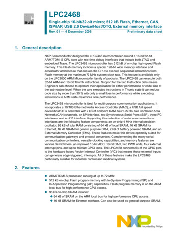
LPC2468NXP SemiconductorsFast communication chip5. Block diagramTMS TDIXTAL1VDD(3V3)XTAL2VDDAtrace signalsP0, P1, P2,P3, P4LPC246864 kBSRAMHIGH-SPEEDGPI/O160 PINSTOTAL512 DMI-SSRAM FLASHEMULATIONTRACE MODULETRST TCK TDOEXTIN0 DBGENRESETPLLSYSTEMFUNCTIONSsystemclockINTERNAL RCOSCILLATORVICEINT3 to EINT0P0, P22 CAP0/CAP1/CAP2/CAP34 MAT2/MAT3,2 MAT0,3 MAT16 PWM0/PWM11 PCAP0,2 PCAP1ETHERNETMAC WITHDMAAHBBRIDGE16 kBSRAMAHB TOAPB BRIDGEUSB DEVICE/HOST/OTG WITH4 kB RAM AND DMAI2SRX CLKI2STX CLKI2SRX WSI2STX WSI2SRX SDAI2STX SDAI2S 3SSP0/SSP1 INTERFACEPWM0, PWM18 AD0A/D CONVERTERSCK0, SCK1MOSI0, MOSI1MISO0, MISO1SSEL0, SSEL1SCKMOSIMIS0SSELSPI INTERFACEMCICLK, MCIPWRSD/MMC CARDINTERFACEMCICMD,MCIDAT[3:0]D/A CONVERTERUART0, UART2, UART3TXD0, TXD2, TXD3RXD0, RXD2, RXD32 kB BATTERY RAMTXD1RXD1DTR1, RTS1power domain 2RTCX1RTCX2VBUSport1port2GP DMACONTROLLEREXTERNAL INTERRUPTSLEGACY GPI/O64 PINS TOTALVBATD[31:0]A[23:0]control linesAHBBRIDGEMASTER AHB TO SLAVEPORT APB BRIDGE PORTP0, P1AOUTEXTERNALMEMORYCONTROLLERAHB1AHB2MII/RMII16 kBSRAMVREFVSSA, R1, CTS1, DCD1,RI1ALARMRD1, RD2TD1, TD2CAN1, CAN2WATCHDOG TIMERSCL0, SCL1, SCL2SDA0, SDA1, SDA2I2C0, I2C1, I2C2SYSTEM CONTROL002aac721Fig 1. LPC2468 block diagramLPC2468 1Preliminary data sheet NXP B.V. 2006. All rights reserved.Rev. 01 — 4 December 20064 of 70
LPC2468NXP SemiconductorsFast communication chip6. Pinning information1572086.1 Pinning1156LPC2468FBD2081055310452002aac734Fig 2. LPC2468 pinning LQFP208 packageball A1index area21436587910 12 14 1611 13 15 nt top viewFig 3. LPC2468 pinning TFBGA208 packageTable 3.Pin allocation tablePin SymbolPin SymbolPin SymbolPin SymbolRow A1P3[27]/D27/CAP1[0]/PWM1[4]2VSSIO3P1[0]/ENET TXD04P4[31]/CS15P1[4]/ENET TX EN6P1[9]/ENET RXD07P1[14]/ENET RX ER8P1[15]/ENET REF CLK/ENET RX CLK9P1[17]/ENET MDIO10P1[3]/ENET /PWM0[5]/DSR114P1[11]/ENET RXD2/MCIDAT2/PWM0[6]15P0[8]/I2STX WS/MISO1/MAT2[2]16P1[12]/ENET RXD3/MCIDAT3/PCAP0[0]LPC2468 1Preliminary data sheet NXP B.V. 2006. All rights reserved.Rev. 01 — 4 December 20065 of 70
LPC2468NXP SemiconductorsFast communication chipTable 3.Pin allocation table continuedPin Symbol17Pin SymbolP1[5]/ENET TX ER/MCIPWR/PWM0[3]Pin Symbol-Pin Symbol--Row B1P3[2]/D22P3[10]/D103P3[1]/D14P3[0]/D05P1[1]/ENET BLS3/MAT2[1]/RXD311P1[6]/ENET TX CLK/MCIDAT0/PWM0[4]12P0[4]/I2SRX CLK---Row 22/PCAP0[0]/RI17P1[8]/ENET CRS DV/ENET CRS8P1[10]/ENET 2/MAT2[0]/TXD312P0[5]/I2SRX WS/TD2/CAP2[1]13P0[7]/I2STX CLK/SCK1 14/MAT2[1]P0[9]/I2STX /A1217VDD(3V3)---Row 3[11]/D116P0[3]/RXD07VDD(3V3)8P3[8]/D89P1[2]/ENET TXD2/MCICLK/PWM0[1]10P1[16]/ENET MDC11VDD(DCDC)(3V3)12VSSCORE13P0[6]/I2SRX SDA/SSEL1/MAT2[0]14P1[7]/ENET 6P1[13]/ENET RX DV17P2[4]/PWM1[5]/DSR1/TRACESYNC---Row PIPESTAT217P2[6]/PCAP1[0]/RI1/TRACEPKT1Row F1P0[25]/AD0[2]/I2SRX 6]/DTR1/TRACEPKT017P3[16]/D16/PWM0[1]/TXD1Row G1P3[5]/D52P0[24]/AD0[1]/I2SRX D2/RTS1/TRACEPKT217P4[10]/A10LPC2468 1Preliminary data sheet NXP B.V. 2006. All rights reserved.Rev. 01 — 4 December 20066 of 70
LPC2468NXP SemiconductorsFast communication chipTable 3.Pin allocation table continuedPin SymbolPin SymbolPin SymbolPin SymbolRow H1P0[23]/AD0[0]/I2SRX ]/U1CONNECT/RXD2/EXTIN017P4[9]/A9Row K0/SCK17P4[8]/A8Row SO0/MISORow A1Row CICMD/SCL1Row 4XTAL214P2[12]/EINT2/MCIDAT2/I2STX 2[28]/DQMOUT0Row P1P1[31]/USB OVRCR2/SCK1/AD0[5]2P1[30]/USB 24]/CKEOUT06VDD(3V3)7P1[18]/USB UP LED1/ 8PWM1[1]/CAP1[0]VDD(3V3)9P1[23]/USB RX P4[19]/A1917VDD(3V3)---Row R1P0[12]/USB PPWR2/MISO1/AD0[6]2P0[13]/USB UP LED2/ /CAP0[1]/PWM1[1]6P0[30]/USB D 17P2[19]/CLKOUT18P1[21]/USB TX DM1/PWM1[3]/SSEL09VSSIO10P1[26]/USB 2[0]/SDA1LPC2468 1Preliminary data sheet NXP B.V. 2006. All rights reserved.Rev. 01 — 4 December 20067 of 70
LPC2468NXP SemiconductorsFast communication chipTable 3.Pin allocation table continuedPin SymbolPin SymbolPin SymbolPin 1]/RXD2/SCL2/MAT3[1]-P4[4]/A4-P4[5]/A5-Row T1P0[27]/SDA02P0[31]/USB D SB HSTEN2/USB CONNECT2/SSEL18P2[20]/DYCS09P1[24]/USB RX DM1/PWM1[5]/MOSI010P1[25]/USB LS1/11USB HSTEN1/MAT1[1]P4[2]/A212P1[27]/USB INT1/USB OVRCR1/CAP0[1]13P1[28]/USB XD2/SDA2/MAT3[0]16P2[13]/EINT3/MCIDAT3/I2STX SDA17P2[11]/EINT1/MCIDAT1/I2STX CLK15---Row U1USB D /USB D 15P2[23]/DYCS3/CAP3[1]/SSEL06P1[19]/USB TX E1/USB PPWR1/CAP1[1]7P1[20]/USB TX DP1/PWM1[2]/SCK08P1[22]/USB RCV1/USB [22]/DYCS2/CAP3[0]/SCK013VDD(3V3)14P1[29]/USB 317P4[16]/A16---6.2 Pin descriptionTable 4.Pin descriptionSymbolPinBallP0[0] to nI/OPort 0: Port 0 is a 32-bit I/O port with individual direction controls for eachbit. The operation of port 0 pins depends upon the pin function selected viathe Pin Connect block.I/OP0[0] — General purpose digital input/output pin.IRD1 — CAN1 receiver input.OTXD3 — Transmitter output for UART3.I/OSDA1 — I2C1 data input/output (this is not an open drain pin).I/OP0[1] — General purpose digital input/output pin.OTD1 — CAN1 transmitter output.IRXD3 — Receiver input for UART3.I/OSCL1 — I2C1 clock input/output (this is not an open drain pin).I/OP0[2] — General purpose digital input/output pin.OTXD0 — Transmitter output for UART0.LPC2468 1Preliminary data sheet NXP B.V. 2006. All rights reserved.Rev. 01 — 4 December 20068 of 70
LPC2468NXP SemiconductorsFast communication chipTable 4.Pin description [1]D6[1]I/OP0[3] — General purpose digital input/output pin.IRXD0 — Receiver input for UART0.P0[4]/I2SRX CLK/RD2/CAP2[0]168[1]B12[1]I/OP0[4] — General purpose digital input/output pin.I/OI2SRX CLK — Receive Clock. It is driven by the master and received bythe slave. Corresponds to the signal SCK in the I2S-bus specification.IRD2 — CAN2 receiver input.P0[5]/I2SRX WS/TD2/CAP2[1]P0[6]/I2SRX SDA/SSEL1/MAT2[0]P0[7]/I2STX CLK/SCK1/MAT2[1]P0[8]/I2STX WS/MISO1/MAT2[2]P0[9]/I2STX AP2[0] — Capture input for Timer 2, channel 0.I/OP0[5] — General purpose digital input/output pin.I/OI2SRX WS — Receive Word Select. It is driven by the master and receivedby the slave. Corresponds to the signal WS in the I2S-bus specification.OTD2 — CAN2 transmitter output.ICAP2[1] — Capture input for Timer 2, channel 1.I/OP0[6] — General purpose digital input/output pin.I/OI2SRX SDA — Receive data. It is driven by the transmitter and read by thereceiver. Corresponds to the signal SD in the I2S-bus specification.I/OSSEL1 — Slave Select for SSP1.OMAT2[0] — Match output for Timer 2, channel 0.I/OP0[7] — General purpose digital input/output pin.I/OI2STX CLK — Transmit Clock. It is driven by the master and received bythe slave. Corresponds to the signal SCK in the I2S-bus specification.I/OSCK1 — Serial Clock for SSP1.OMAT2[1] — Match output for Timer 2, channel 1.I/OP0[8] — General purpose digital input/output pin.I/OI2STX WS — Transmit Word Select. It is driven by the master and receivedby the slave. Corresponds to the signal WS in the I2S-bus specification.I/OMISO1 — Master In Slave Out for SSP1.OMAT2[2] — Match output for Timer 2, channel 2.I/OP0[9] — General purpose digital input/output pin.I/OI2STX SDA — Transmit data. It is driven by the transmitter and read by thereceiver. Corresponds to the signal SD in the I2S-bus specification.I/OMOSI1 — Master Out Slave In for SSP1.OMAT2[3] — Match output for Timer 2, channel 3.I/OP0[10] — General purpose digital input/output pin.OTXD2 — Transmitter output for UART2.I/OSDA2 — I2C2 data input/output (this is not an open drain pin).OMAT3[0] — Match output for Timer 3, channel 0.I/OP0[11] — General purpose digital input/output pin.IRXD2 — Receiver input for UART2.I/OSCL2 — I2C2 clock input/output (this is not an open drain pin).OMAT3[1] — Match output for Timer 3, channel 1.LPC2468 1Preliminary data sheet NXP B.V. 2006. All rights reserved.Rev. 01 — 4 December 20069 of 70
LPC2468NXP SemiconductorsFast communication chipTable 4.Pin description continuedSymbolPinBallTypeDescriptionP0[12]/USB PPWR2/MISO1/AD0[6]41[2]R1[2]I/OP0[12] — General purpose digital input/output pin.OUSB PPWR2 — Port Power enable signal for USB port 2.I/OMISO1 — Master In Slave Out for SSP1.IAD0[6] — A/D converter 0, input 6.I/OP0[13] — General purpose digital input/output pin.OUSB UP LED2 — USB port 2 Good Link LED indicator. It is LOW whendevice is configured (non-control endpoints enabled). It is HIGH when thedevice is not configured or during global suspend.I/OMOSI1 — Master Out Slave In for SSP1.IAD0[7] — A/D converter 0, input 7.I/OP0[14] — General purpose digital input/output pin.OUSB HSTEN2 — Host Enabled status for USB port 2.OUSB CONNECT2 — Soft Connect control for USB port 2. Signal used toswitch an external 1.5 kΩ resistor under software control. Used with theSoftConnect USB feature.I/OSSEL1 — Slave Select for SSP1.I/OP0[15] — General purpose digital input/output pin.OTXD1 — Transmitter output for UART1.I/OSCK0 — Serial clock for SSP0.I/OSCK — Serial clock for SPI.I/OP0 [16] — General purpose digital input/output pin.IRXD1 — Receiver input for UART1.I/OSSEL0 — Slave Select for SSP0.I/OSSEL — Slave Select for SPI.I/OP0[17] — General purpose digital input/output pin.ICTS1 — Clear to Send input for UART1.P0[13]/USB UP LED2/MOSI1/AD0[7]P0[14]/USB HSTEN2/USB 1]J16[1]J14[1]K17[1]K15[1]L17[1]M17[1]I/OMISO0 — Master In Slave Out for SSP0.I/OMISO — Master In Slave Out for SPI.I/OP0[18] — General purpose digital input/output pin.IDCD1 — Data Carrier Detect input for UART1.I/OMOSI0 — Master Out Slave In for SSP0.I/OMOSI — Master Out Slave In for SPI.I/OP0[19] — General purpose digital input/output pin.IDSR1 — Data Set Ready input for UART1.OMCICLK — Clock output line for SD/MMC interface.I/OSDA1 — I2C1 data input/output (this is not an open drain pin).I/OP0[20] — General purpose digital input/output pin.ODTR1 — Data Terminal Ready output for UART1.I/OMCICMD — Command line for SD/MMC interface.I/OSCL1 — I2C1 clock input/output (this is not an open drain pin).LPC2468 1Preliminary data sheet NXP B.V. 2006. All rights reserved.Rev. 01 — 4 December 200610 of 70
LPC2468NXP SemiconductorsFast communication chipTable 4.Pin description IPWR/RD1118[1]M16[1]I/OP0[21] — General purpose digital input/output pin.IRI1 — Ring Indicator input for UART1.OMCIPWR — Power Supply Enable for external SD/MMC power supply.IRD1 — CAN1 receiver input.I/OP0[22] — General purpose digital input/output pin.ORTS1 — Request to Send output for UART1.I/OMCIDAT0 — Data line 0 for SD/MMC interface.OTD1 — CAN1 transmitter output.I/OP0[23] — General purpose digital input/output pin.IAD0[0] — A/D converter 0, input 0.I/OI2SRX CLK — Receive Clock. It is driven by the master and received bythe slave. Corresponds to the signal SCK in the I2S-bus specification.ICAP3[0] — Capture input for Timer 3, channel 0.I/OP0[24] — General purpose digital input/output pin.IAD0[1] — A/D converter 0, input 1.I/OI2SRX WS — Receive Word Select. It is driven by the master and receivedby the slave. Corresponds to the signal WS in the I2S-bus specification.ICAP3[1] — Capture input for Timer 3, channel 1.I/OP0[25] — General purpose digital input/output pin.IAD0[2] — A/D converter 0, input 2.I/OI2SRX SDA — Receive data. It is driven by the transmitter and read by thereceiver. Corresponds to the signal SD in the I2S-bus AD0[0]/I2SRX CLK/CAP3[0]18[2]P0[24]/AD0[1]/I2SRX WS/CAP3[1]16[2]P0[25]/AD0[2]/I2SRX 2][3]T1[4]R3[4]OTXD3 — Transmitter output for UART3.I/OP0[26] — General purpose digital input/output pin.IAD0[3] — A/D converter 0, input 3.OAOUT — D/A converter output.IRXD3 — Receiver input for UART3.I/OP0[27] — General purpose digital input/output pin.I/OSDA0 — I2C0 data input/output. Open drain output (for I2C-buscompliance).I/OP0[28] — General purpose digital input/output pin.I/OSCL0 — I2C0 clock input/output. Open drain output (for I2C-buscompliance).P0[29] — General purpose digital input/output pin.P0[29]/USB D 1 61[5]U4[5]I/OI/OUSB D 1 — USB port 1 bidirectional D line.P0[30]/USB D 1 62[5]R6[5]I/OP0[30] — General purpose digital input/output pin.I/OUSB D 1 — USB port 1bidirectional D line.51[5]T2[5]I/OP0[31] — General purpose digital input/output pin.I/OUSB D 2 — USB port 2 bidirectional D line.I/OPort 1: Port 1 is a 32 bit I/O port with individual direction controls for eachbit. The operation of port 1 pins depends upon the pin function selected viathe Pin Connect block.P0[31]/USB D 2P1[0] to P1[31]LPC2468 1Preliminary data sheet NXP B.V. 2006. All rights reserved.Rev. 01 — 4 December 200611 of 70
LPC2468NXP SemiconductorsFast communication chipTable 4.Pin description continuedSymbolPinBallTypeDescriptionP1[0]/ENET TXD0196[1]A3[1]I/OP1[0] — General purpose digital input/output pin.OENET TXD0 — Ethernet transmit data 0 (RMII/MII interface).P1[1]/ENET TXD1194[1]B5[1]I/OP1[1] — General purpose digital input/output pin.OENET TXD1 — Ethernet transmit data 1 (RMII/MII interface).P1[2]/ENET TXD2/MCICLK/PWM0[1]185[1]I/OP1[2] — General purpose digital input/output pin.OENET TXD2 — Ethernet transmit data 2 (MII interface).OMCICLK — Clock output line for SD/MMC interface.OPWM0[1] — Pulse Width Modulator 0, output 1.I/OP1[3] — General purpose digital input/output pin.OENET TXD3 — Ethernet transmit data 3 (MII interface).I/OMCICMD — Command line for SD/MMC interface.OPWM0[2] — Pulse Width Modulator 0, output 2.I/OP1[4] — General purpose digital input/output pin.OENET TX EN — Ethernet transmit data enable (RMII/MII interface).I/OP1[5] — General purpose digital input/output pin.OENET TX ER — Ethernet Trensmit Error (MII interface).OMCIPWR — Power Supply Enable for external SD/MMC power supply.OPWM0[3] — Pulse Width Modulator 0, output 3.I/OP1[6] — General purpose digital input/output pin.IENET TX CLK — Ethernet Transmit Clock (MII interface).I/OMCIDAT0 — Data line 0 for SD/MMC interface.OPWM0[4] — Pulse Width Modulator 0, output 4.I/OP1[7] — General purpose digital input/output pin.IENET COL — Ethernet Collision detect (MII interface).I/OMCIDAT1 — Data line 1 for SD/MMC interface.OPWM0[5] — Pulse Width Modulator 0, output 5.I/OP1[8] — General purpose digital input/output pin.IENET CRS DV/ENET CRS — Ethernet Carrier Sense/Data Valid (RMIIinterface)/ Ethernet Carrier Sense (MII interface).P1[9] — General purpose digital input/output pin.P1[3]/ENET TXD3/MCICMD/PWM0[2]177[1]D9[1]A10[1]P1[4]/ENET TX EN192[1]A5[1]P1[5]/ENET TX ER/MCIPWR/PWM0[3]156[1]A17[1]P1[6]/ENET TX CLK/MCIDAT0/PWM0[4]171[1]P1[7]/ENET COL/MCIDAT1/PWM0[5]153[1]P1[8]/ENET CRS DV/ENET CRS190[1]P1[9]/ENET RXD0188[1]A6[1]I/OIENET RXD0 — Ethernet receive data 0 (RMII/MII interface).P1[10]/ENET RXD1186[1]C8[1]I/OP1[10] — General purpose digital input/output pin.IENET RXD1 — Ethernet receive data 1 (RMII/MII interface).P1[11]/ENET RXD2/MCIDAT2/PWM0[6]163[1]A14[1]I/OP1[11] — General purpose digital input/output pin.IENET RXD2 — Ethernet Receive Data 2 (MII interface).I/OMCIDAT2 — Data line 2 for SD/MMC interface.OPWM0[6] — Pulse Width Modulator 0, output 6.P1[12]/ENET RXD3/MCIDAT3/PCAP0[0]157[1]I/OP1[12] — General purpose digital input/output pin.IENET RXD3 — Ethernet Receive Data (MII interface).I/OMCIDAT3 — Data line 3 for SD/MMC interface.IPCAP0[0] — Capture input for PWM0, channel 0.B11[1]D14[1]C7[1]A16[1]LPC2468 1Preliminary data sheet NXP B.V. 2006. All rights reserved.Rev. 01 — 4 December 200612 of 70
LPC2468NXP SemiconductorsFast communication chipTable 4.Pin description continuedSymbolPinBallTypeDescriptionP1[13]/ENET RX DV147[1]D16[1]I/OP1[13] — General purpose digital input/output pin.IENET RX DV — Ethernet Receive Data Valid (MII interface).P1[14]/ENET RX ER184[1]A7[1]I/OP1[14] — General purpose digital input/output pin.IENET RX ER — Ethernet receive error (RMII/MII interface).I/OP1[15] — General purpose digital input/output pin.IENET REF CLK/ENET RX CLK — Ethernet Reference Clock (RMIIinterface)/ Ethernet Receive Clock (MII interface).I/OP1[16] — General purpose digital input/output pin.P1[15]/182[1]ENET REF CLK/ENET RX CLKA8[1]P1[16]/ENET MDC180[1]D10[1]IENET MDC — Ethernet MIIM clock.P1[17]/ENET MDIO178[1]A9[1]I/OP1[17] — General purpose digital input/output pin.I/OENET MDIO — Ethernet MI data input and output.P1[18]/USB UP LED1/PWM1[1]/CAP1[0]66[1]P7[1]I/OP1[18] — General purpose digital input/output pin.OUSB UP LED1 — USB port 1 Good Link LED indicator. It is LOW whendevice is configured (non-control endpoints enabled). It is HIGH when thedevice is not configured or during global suspend.OPWM1[1] — Pulse Width Modulator 1, channel 1 output.ICAP1[0] — Capture input for Timer 1, channel 0.I/OP1[19] — General purpose digital input/output pin.P1[19]/USB TX E1/USB PPWR1/CAP1[1]68[1]P1[20]/USB TX DP1/PWM1[2]/SCK070[1]P1[21]/USB TX DM1/PWM1[3]/SSEL072[1]P1[22]/USB RCV1/USB PWRD1/MAT1[0]74[1]P1[23]/USB RX DP1/PWM1[4]/MISO076[1]P1[24]/USB RX 1]OUSB TX E1 — Transmit Enable signal for USB port 1 (OTG transceiver).OUSB PPWR1 — Port Power enable signal for USB port 1.ICAP1[1] — Capture input for Timer 1, channel 1.I/OP1[20] — General purpose digital input/output pin.OUSB TX DP1 — D transmit data for USB port 1 (OTG transceiver).OPWM1[2] — Pulse Width Modulator 1, channel 2 output.I/OSCK0 — Serial clock for SSP0.I/OP1[21] — General purpose digital input/output pin.OUSB TX DM1 — D transmit data for USB port 1 (OTG transceiver).OPWM1[3] — Pulse Width Modulator 1, channel 3 output.I/OSSEL0 — Slave Select for SSP0.I/OP1[22] — General purpose digital input/output pin.IUSB RCV1 — Differential receive data for USB port 1 (OTG transceiver).IUSB PWRD1 — Power Status for USB port 1 (host power switch).OMAT1[0] — Match output for Timer 1, channel 0.I/OP1[23] — General purpose digital input/output pin.IUSB RX DP1 — D receive data for USB port 1 (OTG transceiver).OPWM1[4] — Pulse Width Modulator 1, channel 4 output.I/OMISO0 — Master In Slave Out for SSP0.I/OP1[24] — General purpose digital input/output pin.IUSB RX DM1 — D receive data for USB port 1 (OTG transceiver).OPWM1[5] — Pulse Width Modulator 1, channel 5 output.I/OMOSI0 — Master Out Slave in for SSP0.LPC2468 1Preliminary data sheet NXP B.V. 2006. All rights reserved.Rev. 01 — 4 December 200613 of 70
LPC2468NXP SemiconductorsFast communication chipTable 4.Pin description continuedSymbolPinBallTypeDescriptionP1[25]/USB LS1/USB HSTEN1/MAT1[1]80[1]T10[1]I/OP1[25] — General purpose digital input/output pin.OUSB LS1 — Low Speed status for USB port 1 (OTG transceiver).P1[26]/USB SSPND1/PWM1[6]/CAP0[0]P1[27]/USB INT1/USB OVRCR1/CAP0[1]P1[28]/USB SCL1/PCAP1[0]/MAT0[0]P1[29]/USB SDA1/PCAP1[1]/MAT0[1]P1[30]/USB 2[1]T13[1]U14[1]P2[2]OUSB HSTEN1 — Host Enabled status for USB port 1.OMAT1[1] — Match output for Timer 1, channel 1.I/OP1[26] — General purpose digital input/output pin.OUSB SSPND1 — USB port 1 Bus Suspend status (OTG transciever).OPWM1[6] — Pulse Width Modulator 1, channel 6 output.ICAP0[0] — Capture input for Timer 0, channel 0.I/OP1[27] — General purpose digital input/output pin.IUSB INT1 — USB port 1 OTG ATX interrupt (OTG transceiver).IUSB OVRCR1 — USB port 1 Over-Current status.ICAP0[1] — Capture input for Timer 0, channel 1.I/OP1[28] — General purpose digital input/output pin.I/OUSB SCL1 — USB port 1 I2C serial clock (OTG transciever).IPCAP1[0] — Capture input for PWM1, channel 0.OMAT0[0] — Match output for Timer 0, channel 0.I/OP1[29] — General purpose digital input/output pin.I/OUSB SDA1 — USB port 1 I2C serial data (OTG transciever).IPCAP1[1] — Capture input for PWM1, channel 1.OMAT0[1] — Match output for Timer 0, channel 0.I/OP1[30] — General purpose digital input/output pin.IUSB PWRD2 — Power Status for USB port 2.IVBUS — Indicates the presence of USB bus power.Note: This signal must be HIGH for USB reset to occur.P1[31]/
Real-Time Clock (RTC) with separate power domain, clock source can be the RTC oscillator or the APB clock. 2 kB SRAM powered from the RTC power pin, allowing data to be stored when the rest of the chip is powered off. WatchDog Timer (WDT). The WDT can be clocked from the internal RC oscillator, the RTC oscillator, or the APB clock.