Transcription
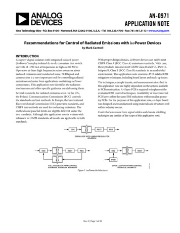
AN-0971APPLICATION NOTEOne Technology Way P.O. Box 9106 Norwood, MA 02062-9106, U.S.A. Tel: 781.329.4700 Fax: 781.461.3113 www.analog.comRecommendations for Control of Radiated Emissions with isoPower Devicesby Mark CantrellINTRODUCTIONiCoupler digital isolators with integrated isolated power(isoPower ) employ isolated dc-to-dc converters that switchcurrents of 700 mA at frequencies as high as 300 MHz.Operation at these high frequencies raises concerns aboutradiated emissions and conducted noise. PCB layout andconstruction is a very important tool for controlling radiatedemissions and noise from applications containing isoPowercomponents. This application note identifies the radiationmechanisms and offers specific guidance on addressing them.Several standards for radiated emissions exist. In the U.S.,the Federal Communications Commission (FCC) controlsthe standards and test methods. In Europe, the InternationalElectrotechnical Commission (IEC) generates standards, andCISPR test methods are used for evaluating emissions. Themethods and pass/fail limits are slightly different under thetwo standards. Although this application note is written withreference to CISPR standards, all results are applicable to bothstandards.OSCWith proper design choices, isoPower devices can easily meetCISPR Class A (FCC Class A) emissions standards. With care,these products can also meet CISPR Class B and FCC Part 15,Subpart B, Class B (FCC Class B) standards in an unshieldedenvironment. This application note examines PCB-related EMImitigation techniques, including board layout and stack-up issues.The techniques, example layouts, and measurements described inthis application note are highly dependent on the options availablein PCB construction. A 4-layer PCB is required to implement theevaluated EMI control techniques. Availability of more internalPCB layers offers the same EMI reductions within smaller geometry PCBs. For the purposes of this application note, a 4-layer boardwas designed and manufactured using materials and structures wellwithin industry norms.Control of emissions from signal cables and chassis shieldingtechniques are outside of the scope of this application note.RECTREGOPEN LOOP WITH LINEAR REGULATORADuM524xRECTREGOSCRECTPWMOPEN LOOP WITH PWM CONTROLADuM5230, ADuM6132FULL FEEDBACK PWM CONTROLADuM540x, ADuM520x, ADuM5000Figure 1. isoPower ArchitecturesRev. C Page 1 of 2007541-001OSC
AN-0971Application NoteTABLE OF CONTENTSIntroduction . 1Recommended Design Practices . 11Revision History . 2Meeting Isolation Standards . 12isoPower Overview. 3Evaluating PCB Structures for EMI . 13Sources of Radiated Emissions . 4Edge Guarding Results . 15Edge Emissions . 4Operating Load and Voltage Dependence . 16Input-to-Output Dipole Emissions . 4Interplane Capacitance . 16Sources of Conducted Noise . 6Integrating Techniques . 17EMI Mitigation Techniques . 7Example 1—Basic Insulation Board . 17Input-to-Output Stitching . 7Example 2—Reinforced Insulation Board . 18Edge Guarding . 8Additional Layout Considerations . 19Interplane Capacitive Bypassing . 9Conclusions . 20Power Reduction . 10References. 20Operating Voltage . 10REVISION HISTORY1/14—Rev. B to Rev. CAdded Table 1 and changes to and moved isoPower OverviewSection . 3Change to Edge Emissions Section . 4Changes to EMI Mitigation Techniques Section . 7Change to Equation 2 . 8Changes to Interplane Capacitive Bypassing Section . 96/11—Rev. A to Rev. BChanges to Introduction Section, isoPower Overview Section,and Figure 1 . 1Changes to Edge Emissions Section and Input-to-OutputDipole Emissions Section . 3Added Figure 3; Renumbered Sequentially . 3Changes to Sources of Conducted Noise Section . 5Deleted Figure 9; Renumbered Sequentially . 5Changes to EMI Mitigation Techniques Section and Input-toOutput Stitching Section . 6Added Safety Rated Capacitor Section and StitchingCapacitance Built into the PCB Section . 6Added Floating Capacitive Structure Section and Gap OverlapStitching Section . 7Replaced Figure 6 and Figure 7 . 7Changes to Edge Guarding Section . 7Deleted Figure 13 . 7Deleted Table 2; Renumbered Sequentially. 8Deleted Figure 15 . 8Changes to Figure 9 and Figure 10 . 8Replaced Buried Capacitance Bypassing Section with InterplaneCapacitive Bypassing Section . 8Added Figure 11. 8Changes to Figure 12 and Power Reduction Section .9Replaced Figure 13 .9Deleted Appendix A—A Design Example Section, Figure 16,and Figure 17.9Added Operating Voltage Section .9Changes to Recommended Design Practices Section . 10Changes to Meeting Isolation Standards Section . 11Added Figure 14 . 11Added Table 1; Renumbered Sequentially . 11Replaced Example Board Section with Evaluating PCBStructures for EMI Section . 12Changes to Figure 15. 12Added Figure 16 and Figure 17 . 12Changes to Table 2. 13Added Stitching Capacitance Results Section, Figure 18, andFigure 19 . 13Added Figure 20, Edge Guarding Results Section, Table 3, andFigure 21 . 14Added Operating Load and Voltage Dependence Section,Figure 22, Figure 23, and Interplane Capacitance Section . 15Added Integrating Techniques Section, Figure 24, Example 1—Basic Insulation Board Section, Table 4, and Figure 25 . 16Added Figure 26 Through Figure 30, Example 2—ReinforcedInsulation Section, and Table 5 . 17Added Additional Layout Considerations Section andFigure 31 . 18Changes to Conclusions Section and References Section . 193/09—Rev. 0 to Rev. A6/08—Revision 0: Initial VersionRev. C Page 2 of 20
Application NoteAN-0971isoPOWER OVERVIEWThe isoPower products shown in Table 1 represent a significantstep forward in isolation technology. Analog Devices, Inc., hasleveraged their experience in micro-transformer design to createchip scale dc-to-dc power converters. These power convertersare incorporated into Analog Devices signal isolation products.Power levels of up to one-half watt are available, at outputvoltages ranging from 3.3 V to 15 V. isoPower is used to powerthe secondary side of the iCoupler data channels as well as toprovide power to off-chip loads.Because the Analog Devices standard data couplers use a similarmagnetic technology, EMI can be an issue in data-only iCouplersand the data channels of isoPower devices. Emissions from datachannels are addressed in the AN-1109 Application Note, Controlof Radiated Emissions in iCoupler Devices.Analog Devices uses several power architectures to achievedesired design goals, such as efficiency, small size, and high outputvoltage (see Figure 1).These architectures have three common elements: a transformerto couple power to the secondary side of the iCoupler, anoscillator tank circuit that switches current into the transformerat an optimum frequency for efficient power transfer, and arectifier that recreates a dc level on the secondary side. Severalregulation methods are used in these products.The physics of the transformer requires that the oscillatorcircuit switch current into the transformer at a rate rangingfrom between 180 MHz and 300 MHz. The rectifier circuit onthe secondary side effectively doubles this frequency during therectification process.These functions are common in switching power supplies;however, the operating frequency is three orders of magnitudehigher than a standard dc-to-dc converter. Noise generated bythe operation of the converter into the 30 MHz to 1 GHz rangeis of concern for radiated emissions.Table 1. isoPower Products that may Require Steps to Control Radiated EmissionsOpen-Loop with LinearRegulatorADuM5240ADuM5241ADuM5242Open-Loop with Primary SidePWM ControlADuM5230ADuM6132High Power Full FeedbackPWM 4Rev. C Page 3 of 20Low Power Full FeedbackPWM M6210ADuM6211ADuM6212
AN-0971Application NoteSOURCES OF RADIATED EMISSIONSEdge emissions occur when unintended currents meet the edgesof ground and power planes. These unintended currents canoriginate from 1 Ground and power noise generated by inadequate bypassof high power current sinks.Cylindrically radiated magnetic fields coming frominductive via penetrations radiated out between boardlayers eventually meeting the board edge.Strip line image charge currents spreading from highfrequency signal lines routed too close to the edge ofthe board.8 16EDGE EMISSIONSdriving the dipole. In many cases, this is a very large dipole asshown in Figure 4. A similar mechanism causes high frequencysignal lines to radiate when crossing splits in the ground andpower planes. This type of radiation is predominantly perpendicular to the gap in the ground planes.9There are two sources of emissions in PCBs where isoPower isused: edge emissions and input-to-output dipole emissions.07541-004Edge emissions are generated (see Figure 2) where differentialnoise from many sources meets the edge of the board, leakingout of a plane-to-plane space and acting as a wave guide.GROUNDPOWER07541-002Figure 4. Dipole Radiation Between Input and OutputFigure 2. Edge Radiation From an Edge Matched Ground Power PairGROUNDPOWER20hSIGNAL07541-003hFigure 3. Edge Radiation From an Edge Mismatched Power Ground PairAt the edge boundary, there are two limiting conditions. Theedges of the ground and power planes are lined up, as shownin Figure 2, or one edge is pulled back by some amount, asshown in Figure 3. In the first case of lined up edges, there issome reflection back into the PCB and some transmission ofthe fields out of the PCB. In the second case, the edge of theboards makes a structure similar to the edge of a patch antenna.When the edges mismatch by 20h, where h is the plane toplane spacing, the fields couple out of the PCB very efficiently,resulting in very high emissions. These two limiting casesbecome important to discussions of edge treatment of the PCB.INPUT-TO-OUTPUT DIPOLE EMISSIONSInput-to-output dipole radiation is generated by driving acurrent source across a gap between ground planes. Thisis the predominant mechanism for radiation for isoPowerapplications. Isolated power supplies, by their very nature,drive energy across gaps in ground planes. The inability ofhigh frequency image charges associated with the power signalto cross the boundary causes differential signals across the gapThe ADuM5400, ADuM5401, ADuM5402, ADuM5403, andADuM5404 devices serves as good examples of the issuesinvolved in generating and mitigating emissions. The oscillatortank circuit in these devices runs at approximately 180 MHz.It can regulate its output to either 5 V or 3.3 V under the controlof a pin on the secondary side. The input voltage can be in the3 V to 5 V range. The highest power operating mode is 5 Vinput and 5 V output and is the primary configurationexamined in this application note.When operating under a full 100 mA output load, the averageinput current is about 290 mA. This means that the peakcurrent in the tank circuit is about twice that value at aswitching rate of 180 MHz.The component’s bypass capacitor is supposed to provide thishigh frequency current locally. This is a lot of current for abypass capacitor to handle. The capacitor must provide largecharge reserves. At the same time, the capacitor must have avery low series resistance at 180 MHz. Even with multiple lowESR capacitors near the pins, an inductively limited bypassallows voltage transients, and the noise is injected onto theground and power planes.Power transfers to the output side where it is rectified into dc.The rectification process doubles the tank frequency to 360 MHz.The input-to-output emissions are both at the rectificationfrequency and the tank frequency, along with some higherharmonics. Figure 5 shows worst-case data collected on a2-layer evaluation board with a near field probe.Rev. C Page 4 of 20
Application Note180MHzTANKAN-0971A board with near field emissions, as shown in Figure 5, andwithout a chassis shield would fail FCC Class B emissionsstandards by approximately 30 dB at the 360 MHz peak.360MHzRECTIFIER07541-005HARMONICS AT540MHz AND720MHzFigure 5. FFT of the Near Field Emissions from a 2-Layer BoardRev. C Page 5 of 20
AN-0971Application NoteSOURCES OF CONDUCTED NOISEThe large currents and frequencies also generate conductednoise on the ground and power planes. This issue is addressedalong with radiated emissions because the causes and remediesfor both types of EMI are addressed with the same PCB groundand power structures.The inability of the bypass capacitors and ground/power planesto provide adequate high frequency current to the isoPower dcto-dc converter causes VDD noise. The dc-to-dc converter switchespower in bursts of 2.5 ns pulses with an amplitude of 700 mA.An ideal bypass capacitor of a few microfarads should be adequate to supply the ac component of the current. Real worldbypass capacitors are not ideal, and they connect to one or,more likely, both of the power planes by an inductive via. Inaddition, a large distance between ground and power planescreates a large inductance between them, restricting their abilityto supply current quickly. These factors contribute to a largefraction of a volt of high frequency noise on the VDD plane.Rev. C Page 6 of 20
Application NoteAN-0971EMI MITIGATION TECHNIQUESMany mitigation techniques are available to the designer.Several techniques that apply directly to the isoPower devicesare identified in this section. The choice of how aggressivelyEMI must be addressed for a design to pass FCC/CISPRemissions levels depends on the requirements of the design aswell as cost and performance tradeoffs. The easiest radiatedEMI mitigation technique to implement is to place the PCB ina grounded chassis with filter elements limiting noise escapingon cable shields. Although this application note does notdescribe this option, note that, where PCB related techniquesare impractical, this method remains available.The EMI mitigation practices rely on having relativelycontinuous ground and power planes and the ability to specifytheir relative positions and distances in the stack-up. Thisdictates that the minimum total number of planes is three:ground, power, and signal planes.For practical considerations in board manufacture, a 4-layerboard is the minimum stack-up. More layers are acceptable andcan be used to greatly enhance the effectiveness of the recommended techniques.The following techniques are effective in reducing EMIradiation and on-board noise: Input-to-output ground plane stitching capacitancePower controlEdge guardingInterplane capacitive bypassCircuit boards with test structures were prepared to evaluateeach of these EMI mitigation techniques utilizing the ADuM5400,ADuM5401, ADuM5402, ADuM5403, and ADuM5404. Thelayout of each board was varied as little as possible to allowmeaningful comparison of results. Testing was conducted at anEMI test facility in a shielded chamber. As expected, duringEMI testing, it was determined that the emissions at the tankfrequency (180 MHz) were predominantly in the plane of theboard, suggesting that the primary mechanism for radiation isfrom the PCB edges. The rectification emissions (360 MHz)are primarily perpendicular to the isolation gap in the board,suggesting input-to-output dipole radiation.INPUT-TO-OUTPUT STITCHINGWhen current flows along PCB traces, an image charge followsalong the ground plane beneath the trace. If the trace crosses agap in the ground plane, the image charge cannot follow along.This creates differential currents and voltages in the PCBleading to radiated and conducted emissions. The solution isto provide a path for the image charge to follow along with thesignal. Standard practice is to place a stitching capacitor inproximity to the signal across the split in the ground plane (seePCB Design for Real-World EMI Control by Archambeault andDrewniak in the References section). This same techniqueworks to minimize radiation between ground planes due to theoperation of isoPower.There are at least three options to form a stitching capacitance. A safety rated capacitor applied across the barrier.A floating metal plane spanning the gap between theisolated and nonisolated sides on an interior layer, asshown in Figure 6.Extending the ground and power planes on an interiorlayer into the isolation gap of the PCB to form a capacitor,as shown in Figure 7.Each of these options has its advantages and disadvantages ineffectiveness and area required to implement.Safety Rated CapacitorA stitching capacitance can be implemented with a simple ceramiccapacitor across the barrier. Capacitors with guaranteed creepage, clearance, and withstand voltage can be obtained frommany major capacitor manufacturers, such as Murata, Johansen,Hitano, and Vishay. Safety rated capacitors are available inseveral grades depending on their intended use. The Y2 gradeis used in line-to-ground applications where there is danger ofelectric shock and is the recommended safety capacitor type fora stitching capacitor in a safety rated application. This type ofcapacitor is available in surface-mount and radial leaded diskversions.Because safety capacitors are discrete components, they mustbe attached to the PCB with pads or through holes. This addsinductance to the capacitor on top of its intrinsic inductance.It also makes the stitching capacitor localized, demanding thatcurrents flow to the capacitor, which can create asymmetricalimage charge paths and added noise. These factors limit theeffectiveness of discrete capacitors to frequencies below about200 MHz.Stitching Capacitance Built into the PCBThe PCB itself can be designed to create a stitching capacitorstructure in several ways. A capacitor is formed when twoplanes in a PCB overlap. In this type of capacitor, theinductance of the parallel plate capacitor formed is extremelylow, and the capacitance is distributed over a large area.These structures must be constructed on internal layers of aPCB. The surface layers have minimum creepage and clearancerequirements; therefore, it is not practical to use surface layersfor this type of structure. This requires a minimum of fourboard layers.A good option is to use a floating metal structure on an interiorlayer of the board to bridge between the primary and secondarypower planes. Note that, hereafter, planes dedicated to groundor power are referred to as reference planes because, from an acnoise point of view, they behave the same and can be used forstitching capacitance interchangeably.Rev. C Page 7 of 20
AN-0971Application NoteFloating Capacitive StructureThis architecture is best suited to applications where a largeramount of board area is available or where reinforced insulationis required.An example of a floating stitching capacitance is shown inFigure 6. The reference planes are shown in blue and green,and the floating coupling plane is shown in yellow. The capacitance of this structure creates two capacitive regions (shownwith shading) linked by the nonoverlapping portion of thestructure. To ensure that optimum capacitance is created forthe area of the structure, the overlap areas of the primary andsecondary sides should be equal.Gap Overlap StitchingA simple method of achieving a good stitching capacitance is toextend a reference plane from the primary and secondary sidesinto the area that is used for creepage on the PCB surface.wIw2w107541-007I07541-006ddFigure 6. Floating Stitching CapacitanceThe capacitive coupling of the structure in Figure 6 is calculatedwith the following basic relationships for parallel plate capacitors:where:C is the total stitching capacitance.AX is the overlap area of the stitching capacitance to eachreference plane.d is the thickness of the insulation layer in the PCB (see Figure 6).ε0 is the permittivity of free space, 8.854 10 12 F/m.εr is the relative permittivity of the PCB insulation material,which is about 4.5 for FR4.lε w 1 w 2 d w1 w 2 (1)where w1, w2, d, and l are the dimensions of the overlappingportions of the floating plane and the primary and secondaryreference planes, as shown in Figure 6.If w1 w2, the equation simplifies toC lw1ε2dThe capacitive coupling of the structure in Figure 7 is calculatedwith the following basic relationships for parallel platecapacitors:C C C2A εC 1, C1 C 2 x , and ε ε0 εrdC1 C 2C Figure 7. Overlapping Plane Stitching Capacitance(2)There are advantages and disadvantages of this structure in realapplications. The major advantage is that there are two isolationgaps, one at the primary and one at the secondary. These gapsare called cemented joints, where the bonding between layersof FR4 provides the isolation. There are also two sequentialpaths through the thickness of the PCB material. The presenceof these gaps and thicknesses is advantageous when creating areinforced isolation barrier under some isolation standards.The disadvantage of this type of structure is that the capacitanceis formed under active circuit area so there can be via penetrations and traces that run across the gaps. Equation 2 also showsthat the capacitance formed is half as effective per unit areaused compared to a simple parallel plate capacitor.Aεand ε ε0 εrd(3)where:C is the total stitching capacitance.d is the thickness of the insulation layer in the PCB,ε0 is the permittivity of free space, 8.854 10 12 F/m.εr is the relative permittivity of the PCB insulation material,which is about 4.5 for FR4.C lwεd(4)where w, d, and l are the dimensions of the overlapping portionof the primary and secondary reference planes, as shown inFigure 7.The major advantage if this structure is that the capacitance iscreated in the gap beneath the isolator, where the top andbottom layers must remain clear for creepage and clearancereasons. This board area is not utilized at all in most designs.The capacitance created is also twice as efficient per unit area asthe floating plane.This architecture has only a single cemented joint and a singlelayer of FR4 between the primary and secondary referenceplanes. It is well suited to smaller boards where only basicinsulation is required.EDGE GUARDINGNoise on the power and ground planes that reaches the edge ofa circuit board can radiate as shown in Figure 2 and Figure 3.If the edge is treated with a shielding structure, the noise isreflected back into the interplane space (see Archambeault andDrewniak in the References section). This can increase thevoltage noise on the planes but reduces edge radiation.Making a solid conductive edge treatment on a PCB is possible,but the process is expensive. A less expensive solution thatRev. C Page 8 of 20
Application NoteAN-0971provide the interplane capacitance layer that supplements thebypass capacitors required for proper operation of the device.works well is to treat the edges of the board with a guard ringstructure laced together by vias. The structure is shown inFigure 8 for a typical 4-layer board. Figure 9 shows how thisstructure can be implemented on the power and ground layersof the primary side of a circuit D07541-010SIGNAL/POWERFigure 10. PCB Stack-Up for Interplane CapacitanceGROUND07541-008POWERGROUND VIA EDGE FENCEAND GUARD RINGS07541-009Figure 8. Via Fence Structure, Side ViewFigure 9. Via Fence and Guard Ring,Shown on the Primary Power Plane LayersThere are two goals in creating edge guarding. The first is to reflectcylindrical emissions from vias back into the interplane space, notallowing it to escape from the edge. The second is to shield anyedge currents flowing on internal planes due to noise or largecurrents.In addition to the ground and power planes, the capacitance canbe increased even further by filling signal layers with alternatingground and power fill. The top and bottom layers in Figure 10are labeled signal/power and signal/ground to illustrate the fillson those particular layers. This has the added benefit of creatingadditional shielding for EMI that leaks around the edges of a viafence structure, keeping it in the PCB. Care must be taken whenmaking ground and power fills. These fills must be tied back tothe full reference plane because a floating fill can act as a patchantenna and radiate instead of shielding. Some recommendedpractices for fills include Fills should be tied to their appropriate reference planealong the edges with vias every 10 mm.Thin fingers of fill should be removed.If the fill has an irregular shape, put vias at the extremeedges of the shape.POWER FILLThe spacing of the vias used to create the edge guard is difficult todetermine without extensive modeling. Analog Devices test boardsused 4 mm via spacing for the evaluation boards. This spacing issmall enough to provide attenuation to signals less than 18 GHz,and it conformed to general guidance from other sources. Thenumber of vias required is reasonable. Further investigation intothe via density was not conducted.AVOID SMALLFILL ISLANDSInterplane capacitance bypassing is a technique intended toreduce both the conducted and radiated emissions of the boardby improving the bypass integrity at high frequencies. This hastwo beneficial effects. First, it reduces the distance that highfrequency noise can spread in the ground and power plane pair.Second, it reduces the initial noise injected into the powerground planes by providing a bypass capacitance that is effective between 200 MHz and 1 GHz (see Archambeault andDrewniak in the References section). Power and ground noisereduction provides a better operating environment for noisesensitive components near the isoPower device. Conductedemissions are reduced proportionate to the reduction in powerand ground noise. The reduction in radiated emissions is not assignificant as that achieved with the stitching or edge guardingtechniques; however, it significantly improves the powerenvironment of the board.VIA TO REFERENCEPLANEGROUNDEDVIA FENCE07541-011INTERPLANE CAPACITIVE BYPASSINGFigure 11. Features of FillThe effectiveness of interplane capacitance is shown in Figure 12.It shows the noise generated by the PWM controlling theprimary side oscillator in a part such as the ADuM5000 or asimilar parts in that series (see Table 1 for a parts list). In thetop section is the noise on the VDD1 pin generated in a 2-layerboard. Th
iso. Power devices can easily meet CISPR Class A (FCC Class A) emissions standards. With care, these products can also meet CISPR Class B and FCC Part 15, Subpart B, Class B (FCC Class B) standards in an unshielded environment. This application note examines PCB-related EMI mitigation techniques , including board layout and stack -up issues.