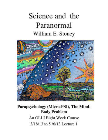
Transcription
EE247Lecture 8 Continuous-time filters continued– Various Gm-C filter implementations– Comparison of continuous-time filter topologies Switched-Capacitor Filters– “Analog” sampled-data filters: Continuous amplitude Quantized time– Applications: First commercial product: Intel 2912 voice-band CODEC chip,1979 Oversampled A/D and D/A converters Stand-alone filtersE.g. National Semiconductor LMF100 (x2 biquads)EECS 247 Lecture 8:Filters: Gm-C & S.C. 2007 H.K. Page 1Summary Last Lecture Automatic on-chip filter tuning (continued from previous lecture)– Continuous tuning Reference integrator locked to a reference frequency DC tuning of resistive timing element– Periodic digitally assisted tuning Systems where filter is followed by ADC & DSP, existing hardwarecan be used to periodically update filter freq. response Continuous-time filters– Highpass filters- 1st orderÆ integrator in the feedback path– Bandpass filters Cascade of LP and HP for Qfilter 5 Direct implementation for narrow-band filter via LP to BPtransformationEECS 247 Lecture 8:Filters: Gm-C & S.C. 2007 H.K. Page 2
Simplest Form of CMOS Gm-CellNonidealities DC gain (integrator Q)a a g0M 1,2 gload(2Lθ Vgs Vth)M 1,2Small Signal Differential Mode Half-CircuitWhere a denotes DC gain & θ is related to channellength modulation by:λ M 1,2gmθLSeems no extra poles!EECS 247 Lecture 8:Filters: Gm-C & S.C. 2007 H.K. Page 3CMOS Gm-Cell High-Frequency PolesCross section view of a MOS transistor operating in saturationDistributed channel resistance & gate capacitance Distributed nature of gate capacitance & channel resistance results ininfinite no. of high-frequency polesEECS 247 Lecture 8:Filters: Gm-C & S.C. 2007 H.K. Page 4
CMOS Gm-Cell High-Frequency Poleseffective P21 1 i 2 P ieffective 2.5ω tM 1,2P2ω tM 1,2 High frequency behavior of an MOStransistor operating in saturation regiong mM 1,23 2 / 3CoxWL2(μ Vgs Vth)M 1,22L Distributed nature of gate capacitance & channel resistance results in aneffective pole at 2.5 times input device cut-off frequencyEECS 247 Lecture 8: 2007 H.K. Page 5Filters: Gm-C & S.C.Simple Gm-Cell Quality Factora (2L)P2effective θ Vgs VthM 1,2int g.Qreal 11 ωoa1 int g.Q154()μ Vgs VthM 1,22L 1pi 2 i (θ Vgs Vth)M 1,22Lωo L2 41 5 μ V Vg s th M 1,2() Note that phase lead associated with DC gain is inversely prop. to L Phase lag due to high-freq. poles directly prop. to LÆ For a given ωο there exists an optimum L which cancel the lead/lagphase error resulting in high integrator QEECS 247 Lecture 8:Filters: Gm-C & S.C. 2007 H.K. Page 6
Simple Gm-Cell Channel Length for OptimumIntegrator Quality Factor1/ 32 θμVVM1,2gsth L.opt. 1 5 4 ωo () Optimum channel length computed based on process parameters (couldvary from process to process)EECS 247 Lecture 8: 2007 H.K. Page 7Filters: Gm-C & S.C.Source-Coupled Pair CMOS Gm-CellTransconductanceFor a source-coupled pair the differential output current (ΔId)as a function of the input voltage(Δvi):Δ vi Δ Id I ss V V gs th() Δ vi 1 1 4 Vgs VthM 1,2 () M 1,2 2 1 / 2 Δ vi Δ IdNote : F or small V V gmM 1,M 2 Δvi gs th M 1,2 Δ IdNot e : A s Δ vi in c re a se so r t heΔ vie ffe c tiv e tra n sc o nd u c ta n c e de c re a se s(EECS 247 Lecture 8:)Filters: Gm-C & S.C.Δ vi Vi1 Vi2Δ Id Id1 Id 2 2007 H.K. Page 8
Source-Coupled Pair CMOS Gm-CellLinearityIdeal Gm gm Large signal Gm drops as input voltage increasesÆ Gives rise to nonlinearityEECS 247 Lecture 8: 2007 H.K. Page 9Filters: Gm-C & S.C.Measure of LinearityVout α1Vin α 2 Vin 2 α 3Vin 3 .Vinamplitude 3rd harmonicdist. comp.HD 3 amplitude fundamental1 α3Vin 2 . 4 α1amplitude 3rd order IM comp.amplitude fundamental3 α325 α5 Vin 2 Vin 4 .4 α18 α1IM 3 EECS 247 Lecture 8:ω1 ω2Filters: Gm-C & S.C.Voutωω1ωVinω1Vout3ω1 ωω1 ω22ω1 ω2ω2ω2 ω1 2007 H.K. Page 10
Source-Coupled Pair Gm-Cell LinearityΔ vi Δ I d I ss V V gs th() Δ vi 1 1 4 Vgs VthM 1,2 () M 1,2 2 1 / 2 ( 1)Δ I d a1 Δ vi a2 Δ vi 2 a3 Δ vi3 . . . . .Se rie sexpansion used in ( 1)I ssa1 & a2 0Vgs VthM 1,2I ssa3 &a4 038 Vgs Vth)()(a5 (M 1,2I ss128 Vgs Vth)&5a6 0M 1,2EECS 247 Lecture 8: 2007 H.K. Page 11Filters: Gm-C & S.C.Linearity of the Source-Coupled Pair CMOS Gm-Cell3a3 2 25a5 4vˆ vˆ . . . .4a1 i8a1 iSu bstitu ting for a1 ,a3 ,. .IM3 24 vˆivˆiIM3 3 25 . . . .32 (VGS Vth ) 1024 (VGS Vth ) v̂i max 4 (VG S Vth ) 2 IM 33I M 3 1% & (VG S Vth ) 1V Vˆinrms 23 0m V Key point: Max. signal handling capability function of gate-overdrive voltageEECS 247 Lecture 8:Filters: Gm-C & S.C. 2007 H.K. Page 12
Simplest Form of CMOS Gm CellDisadvantages Max. signal handling capability function of gate-overdriveIM 3 (VGS Vth ) 2 Critical freq. is also a function of gate-overdriveωo M 1,2gm2 Cint gW V Vgs thLVgs Vthsince gm μ Coxthen ωo (())Æ Filter tuning affects max. signal handling capability!EECS 247 Lecture 8:Filters: Gm-C & S.C. 2007 H.K. Page 13Simplest Form of CMOS Gm CellRemoving Dependence of Maximum Signal HandlingCapability on Tuning Can overcome problem ofmax. signal handlingcapability being a functionof tuning by providingtuning through :– Coarse tuning viaswitching in/out binaryweighted cross-coupledpairsÆ Try to keep gateoverdrive voltageconstant– Fine tuning throughvarying current sourcesÆ Dynamic range dependence on tuning removed (to 1st order)Ref: R.Castello ,I.Bietti, F. Svelto , “High-Frequency Analog Filters in Deep Submicron Technology ,“International Solid State Circuits Conference, pp 74-75, 1999.EECS 247 Lecture 8:Filters: Gm-C & S.C. 2007 H.K. Page 14
Dynamic Range for Source-Coupled Pair Based FilterIM 3 1% & (VGS Vth ) 1V Vinrms 230mV Minimum detectable signal determined by total noise voltage It can be shown for the 6th order Butterworth bandpass filterfundamental noise contribution is given by:vo2 3Q k TCint gAssumin gQ 10Cint g 5 pFrmsvnoise 160 μVrmssince vma x 230mV 3Dynamic Range 20log 230x10 6 63dB160x10EECS 247 Lecture 8:Filters: Gm-C & S.C. 2007 H.K. Page 15Improving the Max. Signal Handling Capability of theSource-Coupled Pair Gm-Cell 2nd source-coupled pair added to subtract current proportional tononlinear component associated with the main SCPI ss1 b &I ss3(Vgs Vth )(Vgs Vth )M 1,2 aand thusM 3,4(WL )(WL )M 1,2 b2aM 3,4EECS 247 Lecture 8:Filters: Gm-C & S.C. 2007 H.K. Page 16
Improving the Max. Signal Handling Capability of theSource-Coupled Pair GmRef: H. Khorramabadi, "High-Frequency CMOS Continuous-Time Filters," U. C. Berkeley, Department ofElectrical Engineering, Ph.D. Thesis, February 1985 (ERL Memorandom No. UCB/ERL M85/19).EECS 247 Lecture 8:Filters: Gm-C & S.C. 2007 H.K. Page 17Improving the Max. Signal Handling Capability of theSource-Coupled Pair Gm Improves maximum signal handling capability by about 12dBÆ Dynamic range theoretically improved to 63 12 75dBEECS 247 Lecture 8:Filters: Gm-C & S.C. 2007 H.K. Page 18
Simplest Form of CMOS Gm-Cell Pros– Capable of very high frequencyperformance (highest?)– Simple design Cons– Tuning affects power dissipation– Tuning affects max. signal handlingcapability (can overcome)– Limited linearity (possible toimprove)Ref: H. Khorramabadi and P.R. Gray, “High Frequency CMOS continuous-time filters,” IEEE Journal ofSolid-State Circuits, Vol.-SC-19, No. 6, pp.939-948, Dec. 1984.EECS 247 Lecture 8:Filters: Gm-C & S.C. 2007 H.K. Page 19Gm-CellSource-Coupled Pair with DegenerationId μ Cox W 2 2 V Vth )Vds Vds ( gs g ds geff 2L I dW V V μ CoxgsthL Vds()Vds small11M3g ds 2M 1,2gmM 1,2M3 g dsfor g mM3geff g dsM3 operating in triode mode Æ source degenerationÆ determines overall gmProvides tuning through varing VcEECS 247 Lecture 8:Filters: Gm-C & S.C. 2007 H.K. Page 20
Gm-CellSource-Coupled Pair with Degeneration Pros– Moderate linearity– Continuous tuning provided byVc– Tuning does not affect powerdissipation Cons– Extra poles associatedwith the source of M1,2,3Æ Low frequencyapplications onlyRef: Y. Tsividis, Z. Czarnul and S.C. Fang, “MOS transconductors and integrators with high linearity,”Electronics Letters, vol. 22, pp. 245-246, Feb. 27, 1986EECS 247 Lecture 8: BiCMOS Gm-CellExampleMOSFET in triode mode:Id μ Cox W 2 (V2L )2 gs Vth Vds Vds Vgs IoutVbLB1XLinearity performance Æ keep gm constantÆfunction of how constant Vds can be held– Need to minimize Gain @ Node XM 1 g B1Ax gmm IsNote that if Vds is kept constant: IWM1 d μ Cox Vdsgm 2007 H.K. Page 21Filters: Gm-C & S.C.Vcm VinM1gm can be varied bychanging Vb and thus VdsSince for a given current, gm of BJT is largercompared to MOS- preferable to use BJTExtra pole at node XEECS 247 Lecture 8:Filters: Gm-C & S.C. 2007 H.K. Page 22
Alternative Fully CMOS Gm-CellExample BJT replaced by a MOStransistor with boosted gm Lower frequency ofoperation compared to theBiCMOS version due tomore parasitic capacitanceat nodes A & BEECS 247 Lecture 8: --AFilters: Gm-C & S.C.B 2007 H.K. Page 23BiCMOS Gm-C Integrator Differential- needs common-modefeedback ckt Freq.tuned by varying VbCintg/2 Design tradeoffs:– Extra poles at the input device drainjunctions– Input devices have to be small tominimize parasitic poles– Results in high input-referred offsetvoltage Æ could drive ckt into nonlinear region– Small devices Æ high 1/f noiseEECS 247 Lecture 8:Filters: Gm-C & S.C.Vout Cintg/2 2007 H.K. Page 24
7th Order Elliptic Gm-C LPFFor CDMA RX Baseband ApplicationVin-A B --A B -- - --A B--A B --A B- A- C- B --A B-Vout Gm-Cell in previous page used to build a 7th order elliptic filter forCDMA baseband applications (650kHz corner frequency) In-band dynamic range of 50dB achievedEECS 247 Lecture 8: 2007 H.K. Page 25Filters: Gm-C & S.C.Comparison of 7th Order Gm-C versus Opamp-RC LPFVinGm-C Filter A- B- A- B--- -- B- A- A- A-- - A- C- B- B- A- B-- B-VoutOpamp-RC Filter - -- -- ------- Vin-- Gm-C filter requires 4times less intg. cap. areacompared to Opamp-RCÆFor low-noiseapplications wherefilter area is dominatedby Cs, could make asignificant differencein the total area Opamp-RC linearitysuperior compared toGm-C Power dissipation tendsto be lower for Gm-Csince OTA load is C andthus no need forbufferingVoEECS 247 Lecture 8:Filters: Gm-C & S.C. 2007 H.K. Page 26
BiCMOS Gm-OTA-C Integrator Used to build filterfor disk-driveapplications Since highfrequency ofoperation, timeconstant sensitivityto parasitic capssignificant.Æ Opamp used M2 & M3 added tocompensate forphase lag (providesphase lead)Ref: C. Laber and P.Gray, “A 20MHz 6th Order BiCMOS Parasitic Insensitive Continuous-time Filter& Second Order Equalizer Optimized for Disk Drive Read Channels,” IEEE Journal of Solid StateCircuits, Vol. 28, pp. 462-470, April 1993.EECS 247 Lecture 8:Filters: Gm-C & S.C. 2007 H.K. Page 276th Order BiCMOS Continuous-time Filter &Second Order Equalizer for Disk Drive Read Channels Gm-C-opamp of the previous page used to build a 6th order filter for DiskDrive Filter consists of 3 Biquad with max. Q of 2 each Performance in the order of 40dB SNDR achieved for up to 20MHzcorner frequencyRef: C. Laber and P.Gray, “A 20MHz 6th Order BiCMOS Parasitic Insensitive Continuous-time Filter& Second Order Equalizer Optimized for Disk Drive Read Channels,” IEEE Journal of Solid StateCircuits, Vol. 28, pp. 462-470, April 1993.EECS 247 Lecture 8:Filters: Gm-C & S.C. 2007 H.K. Page 28
Gm-CellSource-Coupled Pair with Degeneration– Gm-cell intended for low Q disk drive filterRef: I.Mehr and D.R.Welland, "A CMOS Continuous-Time Gm-C Filter for PRML Read ChannelApplications at 150 Mb/s and Beyond", IEEE Journal of Solid-State Circuits, April 1997, Vol.32,No.4, pp. 499-513.EECS 247 Lecture 8:Filters: Gm-C & S.C. 2007 H.K. Page 29Gm-CellSource-Coupled Pair with Degeneration– M7,8 operating in triode mode determine the overall gm of the cell– Feedback provided by M5,6 maintains the gate-source voltage of M1,2 constantby forcing their current to be constantÆ helps linearize rds of M7,8– Current mirrored to the output via M9,10 with a factor of k– Performance level of about 50dB SNDR at fcorner of 25MHz achievedEECS 247 Lecture 8:Filters: Gm-C & S.C. 2007 H.K. Page 30
BiCMOS Gm-C Integrator Needs higher supply voltage comparedto the previous design since quite a fewdevices are stacked vertically M1,2 Æ triode mode Q1,2 Æ hold Vds of M1,2 constant Current ID used to tune filter criticalfrequency by varying Vds of M1,2 andthus controlling gm of M1,2 M3, M4 operate in triode mode andadded to provide common-modefeedbackRef: R. Alini, A. Baschirotto, and R. Castello, “Tunable BiCMOS Continuous-Time Filter for HighFrequency Applications,” IEEE Journal of Solid State Circuits, Vol. 27, No. 12, pp. 19051915, Dec. 1992.EECS 247 Lecture 8: 2007 H.K. Page 31Filters: Gm-C & S.C.BiCMOS Gm-C Integrator M5 & M6 configured ascapacitors- added tocompensate for RHPzero due to Cgd of M1,2(moves it to LHP) sizeof M5,6 Æ 1/3 of M1,21/2CGSM11/3CGSM1M5M1M6M2Ref: R. Alini, A. Baschirotto, and R. Castello, “Tunable BiCMOS Continuous-Time Filter for HighFrequency Applications,” IEEE Journal of Solid State Circuits, Vol. 27, No. 12, pp. 19051915, Dec. 1992.EECS 247 Lecture 8:Filters: Gm-C & S.C. 2007 H.K. Page 32
BiCMOS Gm-C Filter For Disk-Drive Application Using the integrators shown in the previous pageBiquad filter for disk drivesgm1 gm2 gm4 2gm3Q 2Tunable from 8MHz to 32MHzRef: R. Alini, A. Baschirotto, and R. Castello, “Tunable BiCMOS Continuous-Time Filter for HighFrequency Applications,” IEEE Journal of Solid State Circuits, Vol. 27, No. 12, pp. 1905-1915,Dec. 1992.EECS 247 Lecture 8:Filters: Gm-C & S.C. 2007 H.K. Page 33SummaryContinuous-Time Filters Opamp RC filters– Good linearity Æ High dynamic range (60-90dB)– Only discrete tuning possible– Medium usable signal bandwidth ( 10MHz) Opamp MOSFET-C– Linearity compromised (typical dynamic range 40-60dB)– Continuous tuning possible– Low usable signal bandwidth ( 5MHz) Opamp MOSFET-RC– Improved linearity compared to Opamp MOSFET-C (D.R. 50-90dB)– Continuous tuning possible– Low usable signal bandwidth ( 5MHz) Gm-C– Highest frequency performance (at least an order of magnitude highercompared to the rest 100MHz)– Dynamic range not as high as Opamp RC but better than OpampMOSFET-C (40-70dB)EECS 247 Lecture 8:Filters: Gm-C & S.C. 2007 H.K. Page 34
Switched-Capacitor FiltersToday Emulating resistor via switched-capacitor network 1st order switched-capacitor filter Switch-capacitor filter considerations:––––Issue of aliasing and how to avoid itTradeoffs in choosing sampling rateEffect of sample and holdSwitched-capacitor filter electronic noiseEECS 247 Lecture 8: 2007 H.K. Page 35Filters: Gm-C & S.C.Switched-Capacitor Resistor Capacitor C is the “switchedcapacitor”vIN Non-overlapping clocks φ1 and φ2control switches S1 and S2,respectivelyφ1φ2S1S2vOUTC vIN is sampled at the falling edge ofφ1– Sampling frequency fS Next, φ2 rises and the voltageacross C is transferred to vOUT Why does this behave as aresistor?EECS 247 Lecture 8:φ1φ2T 1/fsFilters: Gm-C & S.C. 2007 H.K. Page 36
Switched-Capacitor Resistors Charge transferred from vIN tovOUT during each clock cycle is:vINQ C(vIN – vOUT)φ1φ2S1S2vOUTC Average current flowing fromvIN to vOUT is:i Q/t Q . fsφ1Substituting for Q:φ2i fS C(vIN – vOUT)EECS 247 Lecture 8:T 1/fs 2007 H.K. Page 37Filters: Gm-C & S.C.Switched-Capacitor Resistorsi fS C(vIN – vOUT)With the current through the switchedcapacitor resistor proportional to thevoltage across it, the equivalent“switched capacitor resistance” is:vINS1S2vOUTφ1Note: Can build large time-constant insmall areaEECS 247 Lecture 8:φ2CReq VIN iVOUT 1f sCExample:f s 100KHz ,C 0.1pF Req 100Mega Ωφ1φ2Filters: Gm-C & S.C.T 1/fs 2007 H.K. Page 38
Switched-Capacitor Filter Let’s build a “switched- capacitor ”filter REQvINvOUTC2 Start with a simple RC LPF Replace the physical resistor byan equivalent switched-capacitorresistor 3-dB bandwidth:Cω 3dB 1 f s 1ReqC2C2Cf 3dB 1 f s 12πC2EECS 247 Lecture 8:vINφ1φ2S1S2vOUTC1C2 2007 H.K. Page 39Filters: Gm-C & S.C.Switched-Capacitor Filter Advantage versusContinuous-Time Filterφ1Reqφ2VinS1S2C1VoutVinC2C2f 3 dB f 3dB 1 f s C12πC2 Corner freq. proportional to:System clock (accurate to few ppm)C ratio accurate Æ 0.1%Vout11 2π ReqC2 Corner freq. proportional to:Absolute value of Rs & CsPoor accuracy Æ 20 to 50%³ Main advantage of SC filtersÆ inherent corner frequency accuracyEECS 247 Lecture 8:Filters: Gm-C & S.C. 2007 H.K. Page 40
Typical Sampling ProcessContinuous-Time(CT) Sampled Data (SD)ContinuousTime SignaltimeSampled DataSampled Data ZOHClockEECS 247 Lecture 8: 2007 H.K. Page 41Filters: Gm-C & S.C.Uniform SamplingContinuous time signal xc(t)Sampling intervalTSampling frequencyfs 1/TSampled signalxd(kT) x(k)AmplitudeNomenclature:xc(t) Problem: Multiple continuous timesignals can yield exactly the samediscrete time signal Let’s look at samples taken at 1μsintervals of several sinusoidalwaveforms xd(kT)TtimeNote: Samples are the waveform values at kT instancesand undefined in betweenEECS 247 Lecture 8:Filters: Gm-C & S.C. 2007 H.K. Page 42
voltageSampling Sine WavesT 1μsfs 1/T 1MHzfin 101kHztimey(nT)v(t ) cos ( 2π .fi n .t )Sampled-data domian t n.T or t n/fsfi n 101kHz .n cos 2π .n v(n) cos 2π .fs 1MHz EECS 247 Lecture 8: 2007 H.K. Page 43Filters: Gm-C & S.C.Sampling Sine WavesAliasingvoltageT 1μsfs 1/T 1MHzfin 899kHztime101kHz 89 9 k H z (1 0 0 0 k Hz - 1 0 1k Hz ) . n c o s 2π . n c o s 2π .n v ( n ) c o s 2π . 1M Hz1M Hz1M Hz 101kHz .n c os 2π . 1MHzEECS 247 Lecture 8:Filters: Gm-C & S.C. 2007 H.K. Page 44
Sampling Sine WavesAliasingvoltageT 1μsfs 1/T 1MHzfin 1101kHztime(1000kHz 101kHz ) 1101kHz .n co s 2π .n v( n) cos 2π . 1MHz1MHz101kHz .n cos 2π . 1 MHzEECS 247 Lecture 8:Filters: Gm-C & S.C. 2007 H.K. Page 45Sampling Sine WavesProblem:Identical samples for:v(t) cos [2π fint ]v(t) cos [2π( fin n.fs )t ]v(t) cos [2π( fin-n.fs )t ]* (n-integer)ÆMultiple continuous time signals can yieldexactly the same discrete time signalEECS 247 Lecture 8:Filters: Gm-C & S.C. 2007 H.K. Page 46
Sampling Sine WavesFrequency SpectrumContinuous-TimeAmplitudeSignal scenariobefore samplingfs finfs – fin1101kHz899kHzfsfin1MHz101kHz2fs fSignal scenarioafter samplingAmplitudeDiscrete Time0.5f /fsKey point: Signals @ nfS fmax signal fold back into band of interestÆAliasingEECS 247 Lecture 8:Filters: Gm-C & S.C. 2007 H.K. Page 47Aliasing Multiple continuous time signals can produceidentical series of samples The folding back of signals from nfs fsig (n integer)down to ffin is called aliasing– Sampling theorem: fs 2fmax Signal If aliasing occurs, no signal processing operationdownstream of the sampling process can recoverthe original continuous time signalEECS 247 Lecture 8:Filters: Gm-C & S.C. 2007 H.K. Page 48
How to Avoid Aliasing? Must obey sampling theorem:fmax-Signal fs /2*Note:Minimum sampling rate of fs 2xfmax-Signal is called Nyquist rate Two possibilities:1. Sample fast enough to cover all spectral components,including "parasitic" ones outside band of interest2. Limit fmax Signal through filtering Æ attenuate out-of-bandcomponents prior to samplingEECS 247 Lecture 8: 2007 H.K. Page 49Filters: Gm-C & S.C.How to Avoid Aliasing?1-Sample FastAmplitudeFrequency domainfinfs old2fs old .fs newfPush sampling frequency to x2 of the highestfrequency signal to cover all unwanted signals aswell as wanted signalsÆ In vast majority of cases not practicalEECS 247 Lecture 8:Filters: Gm-C & S.C. 2007 H.K. Page 50
How to Avoid Aliasing?2-Filter Out-of-Band Signal Prior to SamplingAmplitudeFrequency domainfinfs2fs .FilterFrequency domainAmplitudefinfs /2ffs2fs .fPre-filter signal to eliminate/attenuate signals above fs/2- then sampleEECS 247 Lecture 8: 2007 H.K. Page 51Filters: Gm-C & S.C.Anti-Aliasing Filter asingPre-Filter0fs /2fsRealisticAnti-AliasingPre-Filter2fs.fCase1- B fsigmax fs /2 Non-practical since an extremely high order anti-aliasing filter (close toan ideal brickwall filter) is requiredPractical anti-aliasing filter ÆNon-zero filter "transition band"In order to make this work, we need to sample much faster than 2x thesignal bandwidthÆ"Oversampling"EECS 247 Lecture 8:Filters: Gm-C & S.C. 2007 H.K. Page 52
Practical Anti-Aliasing -CapacitorFilterParasiticToneAttenuationCase2 - B fmax Signal fs/2More practical anti-aliasing filterPreferable to have an antialiasing filter with:ÆThe lowest order possibleÆNo frequency tuning required(if frequency tuning isrequired then why useswitched-capacitor filter, justuse the prefilter!?)EECS 247 Lecture 8:0B0 B/fsfs /2fs -Bfs0.5Filters: Gm-C & S.C. ff./fs 2007 H.K. Page 53TradeoffOversampling Ratio versus Anti-Aliasing Filter OrderMaximumAliasedSignalRejectionFilter Orderfs /fin-max* AssumptionÆ anti-aliasing filter is Butterworth type (not a necessary requirement)ÆTradeoff:Sampling speed versus anti-aliasing filter orderRef: R. v. d. Plassche, CMOS Integrated Analog-to-Digital and Digital-to-Analog Converters, 2nded., Kluwer publishing, 2003, p.41]EECS 247 Lecture 8:Filters: Gm-C & S.C. 2007 H.K. Page 54
Effect of Sample & Hold.Sample &Hold.TpTsTs Using the Fourier transform of a rectangular impulse:H( f ) EECS 247 Lecture 8:Tp sin(πfT p )πfT pTs 2007 H.K. Page 55Filters: Gm-C & S.C.Effect of Sample & Hold onFrequency Response1abs(H(f))0.90.8 H ( f ) 0.7Tp TsT p sin(πfT p )TsπfT pf Tp )f s Tsfπfssin(π More practical0.60.5Tp 0.5Ts0.40.30.20.10EECS 247 Lecture 8:00.511.5f / fsFilters: Gm-C & S.C.22.53 2007 H.K. Page 56
Sample & Hold Effect(Reconstruction of Analog Signals)Time domainTp TsMagnitudedroop dueto sinx/xeffectEECS 247 Lecture 8:timeZOHAmplitudevoltageTp TsH( f ) finsin(π fTs )π fTsFrequency domain2fs . ffs 2007 H.K. Page 57Filters: Gm-C & S.C.Sample & Hold Effect(Reconstruction of Analog Signals)Droop -1dBVoltageCase 1) fsig fs /4Time domaintimeAmplitudeMagnitude droopdue to sinx/xeffect:-1dBfinEECS 247 Lecture 8:Filters: Gm-C & S.C.Frequency domainfsf 2007 H.K. Page 58
Sample & Hold Effect(Reconstruction of Analog Signals)Time domainMagnitude droop dueto sinx/x effect:10.80.60.4Case 2)Amplitude0.2fsig fs /320-0.2-0.4-0.6-0.8sampled dataafter ZOH-100.511.52Time-0.0035dBAmplitudeDroop -0.0035dBÆ Highoversampling ratiodesirablefinEECS 247 Lecture 8:2.533.5x 10-5Frequency domainfsf 2007 H.K. Page 59Filters: Gm-C & S.C.Sampling Process Including S/HH(Z)e.g. inGeneralSignalfinfBEECS 247 Lecture 8:ffs2fsfs2fsfs2fsfs2fsFilters: Gm-C & S.C.fsfs2fs2fs 2007 H.K. Page 60
Simple Gm-Cell Channel Length for Optimum Integrator Quality Factor ()2 1/3 M1,2 o. 15 VVgs th Lopt. 4 . Id 2VVVVgs th ds ds 2L g Id C W VV ds ox gs th VLds 1 g 12 gg for g g gg