Transcription
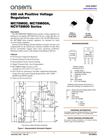
DATA SHEETwww.onsemi.com500 mA Positive VoltageRegulators4MC78M00, MC78M00A,NCV78M00 Series1 2DescriptionThe MC78M00/MC78M00A Series positive voltage regulators areidentical to the popular MC7800 Series devices, except that they arespecified for only half the output current. Like the MC7800 devices,the MC78M00 three terminal regulators are intended for local,on card voltage regulation.Internal current limiting, thermal shutdown circuitry and safe areacompensation for the internal pass transistor combine to make thesedevices remarkably rugged under most operating conditions.Maximum output current, with adequate heatsinking is 500 mA. Input1.0 k2106.7V 16 k3001.0 k3.6k2003.0 k30010 pF6.4k5.6 k0.24132.6 k520502.0 k6.0 k200MC78MxxXXTAWLYWWGHeatsink surfaceconnected to Pin 2.xxXXAWLYWWG Voltage Option Appropriate Suffix Options Assembly Location Wafer Lot Year Work Week Pb Free PackageHeatsink surface (shown as terminal 4 incase outline drawing) is connected to Pin 2. Device Type and Voltage Option Code Assembly Location Wafer Lot Year Work Week Pb Free PackagePin 1. Input2. Ground3. OutputOutput40pFORDERING INFORMATIONSee detailed ordering and shipping information in the packagedimensions section on page 10 14 of this data sheet.3.9 k6.0k3TO 220T SUFFIXCASE 221ABxxxxxGALYWWxxxxxALYWWG1002MARKINGDIAGRAMSNo External Components RequiredInternal Thermal Overload ProtectionInternal Short Circuit Current LimitingOutput Transistor Safe Area CompensationMC78M00A High Accuracy ( 2%)Available for 5.0 V, 8.0 V, 12 V and 15 VNCV Prefix for Automotive and Other Applications RequiringUnique Site and Control Change Requirements; AEC Q100Qualified and PPAP CapableThese are Pb Free Devices1.0 k1DPAK 3DT SUFFIXCASE 369CFeatures 3DEVICE MARKING INFORMATION2.8 kGNDSee general marking information in the device markingsection on page 10 of this data sheet.This device contains 28 active transistors.Figure 1. Representative Schematic Diagram Semiconductor Components Industries, LLC, 2016November, 2021 Rev. 291Publication Order Number:MC78M00/D
MC78M00, MC78M00A, NCV78M00 SeriesMAXIMUM RATINGS (TA 25 C, unless otherwise noted) (Note 1)SymbolRatingInput Voltage(5.0 V 18 V)(20 V 24V)ValueVIPower Dissipation (Package Limitation)Plastic Package, T SuffixTA 25 CThermal Resistance, Junction-to-AirThermal Resistance, Junction-to-CasePlastic Package, DT SuffixTA 25 CThermal Resistance, Junction-to-AirThermal Resistance, Junction-to-CaseUnitVdc3540 C/WPDqJAqJCInternally Limited705.0PDqJAqJCInternally Limited925.0Operating Junction Temperature RangeTJ 150 CStorage Temperature RangeTstg 65 to 150 CStresses exceeding those listed in the Maximum Ratings table may damage the device. If any of these limits are exceeded, device functionalityshould not be assumed, damage may occur and reliability may be affected.1. This device series contains ESD protection and exceeds the following tests:Human Body Model 2000 V per MIL STD 883, Method 3015.Machine Model Method 200 V.MC78M05C/AC/B/AB, NCV78M05AB/B ELECTRICAL CHARACTERISTICS(VI 10 V, IO 350 mA, TJ Tlow to Thigh, PD 5 W, unless otherwise noted) (Note 2)SymbolCharacteristicsOutput Voltage (TJ 25 CV78M05ABVOOutput Voltage Variation (7.0 Vdc VI 20 Vdc, 5.0 mA IO 350 NCV78M05ABVOLine Regulation (TJ 25 C, 7.0 Vdc VI 25 Vdc, IO 200 mA)ReglineLoad Regulation(TJ 25 C, 5.0 mA IO 500 mA)(TJ 25 C, 5.0 mA IO 200 mA)RegloadInput Bias Current (TJ 25 C)IIBQuiescent Current Change(8.0 Vdc VI 25 Vdc, IO 200 mA)(5.0 mA IO 350 mA)DIIBOutput Noise Voltage (TA 25 C, 10 Hz f 100 kHz)VnRipple Rejection(IO 100 mA, f 120 Hz, 8.0 V VI 18 V)(IO 300 mA, f 120 Hz, 8.0 VI 18 V, TJ 25 C)RRDropout Voltage (TJ 25 C)Short Circuit Current Limit (TJ 25 C, VI 35 V)Average Temperature Coefficient of Output Voltage (IO 5.0 mA)Peak Output Current(TJ 25 C)2. Tlow 0 C for MC78MxxAC, C 40 C for MC78MxxAB, B, NCV78MxxAB, BThigh 125 C for MC78MxxAB, AC, B, C, NCV78MxxAB, 0 5.255.20 3.050 201010050 3.26.0 0.80.5 40 6262 80 UnitVdcVdcmVmVmAmAmVdBVI VO 2.0 VdcIOS 350 mADVO/DT 0.2 mV/ CIO 700 mA
MC78M00, MC78M00A, NCV78M00 SeriesMC78M06C/B ELECTRICAL CHARACTERISTICS(VI 11 V, IO 350 mA, TJ Tlow to Thigh, PD 5.0 W, unless otherwise noted) (Note 3)CharacteristicsSymbolMinTypMaxUnitOutput Voltage (TJ 25 C)VO5.756.06.25VdcOutput Voltage Variation (8.0 Vdc VI 21 Vdc, 5.0 mA IO 350 mA)VO5.7 6.3VdcLine Regulation (TJ 25 C, 8.0 Vdc VI 25 Vdc, IO 200 mA)Regline 5.050mVLoad Regulation(TJ 25 C, 5.0 mA IO 500 Ma)(TJ 25 C, 5.0 mA IO 200 mA)Regload 201012060 3.26.0 0.80.5 45 5959 80 VI VO 2.0 VdcIOS 350 mADVO/DT 0.2 mV/ CIO 700 mASymbolMinTypMaxUnit7.707.848.08.08.308.167.67.7 8.48.3 6.050 251016080 3.26.0 0.80.5 52 5656 80 VI VO 2.0 VdcIOS 350 mADVO/DT 0.2 mV/ CIO 700 mAInput Bias Current (TJ 25 C)IIBQuiescent Current Change(9.0 Vdc VI 25 Vdc, IO 200 mA)(5.0 mA IO 350 mA)DIIBOutput Noise Voltage (TA 25 C, 10 Hz f 100 kHz)VnRipple Rejection(IO 100 mA, f 120 Hz, 9.0 V VI 19 V)(IO 300 mA, f 120 Hz, 9.0 V VI 19 V, TJ 25 C)RRDropout Voltage (TJ 25 C)Short Circuit Current Limit (TJ 25 C, VI 35 V)Average Temperature Coefficient of Output Voltage (IO 5.0 mA)Peak Output Current (TJ 25 C)mVmAmAmVdBMC78M08C/AC/B/AB, NCV78M08B ELECTRICAL CHARACTERISTICS(VI 14 V, IO 350 mA, TJ Tlow to Thigh, PD 5 W, unless otherwise noted) (Note 3)CharacteristicsOutput Voltage (TJ 25 Output Voltage Variation (10.5 Vdc VI 23 Vdc, 5.0 mA IO 350 OLine Regulation (TJ 25 C, 10.5 Vdc VI 25 Vdc, IO 200 mA)ReglineLoad Regulation(TJ 25 C, 5.0 mA IO 500 mA)(TJ 25 C, 5.0 mA IO 200 mA)RegloadInput Bias Current (TJ 25 C)IIBQuiescent Current Change(10.5 Vdc VI 25 Vdc, IO 200 mA)(5.0 mA IO 350 mA)DIIBOutput Noise Voltage (TA 25 C, 10 Hz f 100 kHz)VnRipple Rejection(IO 100 mA, f 120 Hz, 11.5 V VI 21.5 V)(IO 300 mA, f 120 Hz, 11.5 V VI 21.5 V, TJ 25 C)RRDropout Voltage (TJ 25 C)Short Circuit Current Limit (TJ 25 C, VI 35 V)Average Temperature Coefficient of Output Voltage (IO 5.0 mA)Peak Output Current (TJ 25 C)3. Tlow 0 C for MC78MxxAC, C 40 C for MC78MxxAB, B, NCV78MxxAB, BThigh 125 C for MC78MxxAB, AC, B, C, NCV78MxxAB, Bwww.onsemi.com3VdcVdcmVmVmAmAmVdB
MC78M00, MC78M00A, NCV78M00 SeriesMC78M09C/B, NCV78M09B ELECTRICAL CHARACTERISTICS(VI 15 V, IO 350 mA, TJ Tlow to Thigh, PD 5.0 W, unless otherwise noted) (Note 4)CharacteristicsSymbolMinTypMaxUnitOutput Voltage (TJ 25 C)VO8.649.09.45VdcOutput Voltage Variation (11.5 Vdc VI 23 Vdc, 5.0 mA IO 350 mA)VO8.55 9.45VdcLine Regulation (TJ 25 C, 11.5 Vdc VI 25 Vdc, IO 200 mA)Regline 6.050mVLoad Regulation(TJ 25 C, 5.0 mA IO 500 mA)(TJ 25 C, 5.0 mA IO 200 mA)Regload 251018090 3.26.0 0.80.5 52 5656 80 VI VO 2.0 VdcIOS 350 mADVO/DT 0.2 mV/ CIO 700 1.5 12.612.5 8.050 2510240120 3.26.0 0.80.5 75 5555 80 VI VO 2.0 VdcIOS 350 mADVO/DT 0.3 mV/ CIO 700 mAInput Bias Current (TJ 25 C)IIBQuiescent Current Change(11.5 Vdc VI 25 Vdc, IO 200 mA)(5.0 mA IO 350 mA)DIIBOutput Noise Voltage (TA 25 C, 10 Hz f 100 kHz)VnRipple Rejection(IO 100 mA, f 120 Hz, 12.5 V VI 22.5 V)(IO 300 mA, f 120 Hz, 12.5 V VI 22.5 V, TJ 25 C)RRDropout Voltage (TJ 25 C)Short Circuit Current Limit (TJ 25 C, VI 35 V)Average Temperature Coefficient of Output Voltage (IO 5.0 mA)Peak Output Current (TJ 25 C)mVmAmAmVdBMC78M12C/AC/B/AB, NCV78M12B ELECTRICAL CHARACTERISTICS(VI 19 V, IO 350 mA, TJ Tlow to Thigh, PD 5 W, unless otherwise noted) (Note 4)CharacteristicsOutput Voltage (TJ 25 Output Voltage Variation (14.5 Vdc VI 27 Vdc, 5.0 mA IO 350 OLine Regulation (TJ 25 C, 14.5 Vdc VI 30 Vdc, IO 200 mA)ReglineLoad Regulation(TJ 25 C, 5.0 mA IO 500 mA)(TJ 25 C, 5.0 mA IO 200 mA)RegloadInput Bias Current (TJ 25 C)IIBQuiescent Current Change(14.5 Vdc VI 30 Vdc, IO 200 mA)(5.0 mA IO 350 mA)DIIBOutput Noise Voltage (TA 25 C, 10 Hz f 100 kHz)VnRipple Rejection(IO 100 mA, f 120 Hz, 15 V VI 25 V)(IO 300 mA, f 120 Hz, 15 V VI 25 V, TJ 25 C)RRDropout Voltage (TJ 25 C)Short Circuit Current Limit (TJ 25 C, VI 35 V)Average Temperature Coefficient of Output Voltage (IO 5.0 mA)Peak Output Current (TJ 25 C)4. Tlow 0 C for MC78MxxAC, C 40 C for MC78MxxAB, B, NCV78MxxAB, BThigh 125 C for MC78MxxAB, AC, B, C, NCV78MxxAB, Bwww.onsemi.com4VdcVdcmVmVmAmAmVdB
MC78M00, MC78M00A, NCV78M00 SeriesMC78M15C/AC/B/AB, NCV78M15B ELECTRICAL CHARACTERISTICS(VI 23 V, IO 350 mA, TJ Tlow to Thigh, PD 5 W, unless otherwise noted) (Note .314.2514.40 15.7515.60 1050 2510300150 3.26.0 0.80.5 90 5454 70 VI VO 2.0 VdcIOS 350 mADVO/DT 0.3 mV/ CIO 700 mAOutput Voltage (TJ 25 Output Voltage Variation (17.5 Vdc VI 30 Vdc, 5.0 mA IO 350 OInput Regulation (TJ 25 C, 17.5 Vdc VI 30 Vdc, IO 200 mA)ReglineLoad Regulation(TJ 25 C, 5.0 mA IO 500 mA)(TJ 25 C, 5.0 mA IO 200 mA)RegloadInput Bias Current (TJ 25 C)IIBQuiescent Current Change(17.5 Vdc VI 30 Vdc, IO 200 mA)(5.0 mA IO 350 mA)DIIBOutput Noise Voltage (TA 25 C, 10 Hz f 100 kHz)VnRipple Rejection(IO 100 mA, f 120 Hz, 18.5 V VI 28.5 V)(IO 300 mA, f 120 Hz, 18.5 V VI 28.5 V, TJ 25 C)RRDropout Voltage (TJ 25 C)Short Circuit Current Limit (TJ 25 C, VI 35 V)Average Temperature Coefficient of Output Voltage (IO 5.0 mA)Peak Output Current (TJ 25 C)UnitVdcVdcmVmVmAmAmVdBMC78M18C/B ELECTRICAL CHARACTERISTICS(VI 27 V, IO 350 mA, TJ Tlow to Thigh, PD 5 W, unless otherwise noted) (Note 5)CharacteristicsSymbolMinTypMaxUnitOutput Voltage (TJ 25 C)VO17.31818.7VdcOutput Voltage Variation (21 Vdc VI 33 Vdc, 5.0 mA IO 350 mA)VO17.1 18.9VdcLine Regulation (TJ 25 C, 21 Vdc VI 33 Vdc, IO 200 mA)Regline 1050mVLoad Regulation(TJ 25 C, 5.0 mA IO 500 mA)(TJ 25 C, 5.0 mA IO 200 mA)Regload 3010360180 3.26.5 0.80.5 100 Input Bias Current (TJ 25 C)IIBQuiescent Current Change(21 Vdc VI 33 Vdc, IO 200 mA)(5.0 mA IO 350 mA)DIIBOutput Noise Voltage (TA 25 C, 10 Hz f 100 kHz)VnRipple Rejection(IO 100 mA, f 120 Hz, 22 V VI 32 V)(IO 300 mA, f 120 Hz, 22 V VI 32 V, TJ 25 C)RRDropout Voltage (TJ 25 C)Short Circuit Current Limit (TJ 25 C, VI 35 V)Average Temperature Coefficient of Output Voltage (IO 5.0 mA)Peak Output Current (TJ 25 C)5. Tlow 0 C for MC78MxxAC, C 40 C for MC78MxxAB, B, NCV78MxxAB, BThigh 125 C for MC78MxxAB, AC, B, C, NCV78MxxAB, Bwww.onsemi.com5mVmAmAmVdB5353 70 VI VO 2.0 VdcIOS 350 mADVO/DT 0.3 mV/ CIO 700 mA
MC78M00, MC78M00A, NCV78M00 SeriesMC78M20C/B ELECTRICAL CHARACTERISTICS(VI 29 V, IO 350 mA, TJ Tlow to Thigh, PD 5.0 W, unless otherwise noted) (Note 6)CharacteristicsSymbolMinTypMaxUnitOutput Voltage (TJ 25 C)VO19.22020.8VdcOutput Voltage Variation (23 Vdc VI 35 Vdc, 5.0 mA IO 350 mA)VO19 21VdcLine Regulation (TJ 25 C, 23 Vdc VI 35 Vdc, IO 200 mA)Regline 1050mVLoad Regulation(TJ 25 C, 5.0 mA IO 500 mA)(TJ 25 C, 5.0 mA IO 200 mA)Regload 3010400200 3.26.5 0.80.5 110 5252 70 VI VO 2.0 VdcIOS 350 mADVO/DT 0.5 mV/ CIO 700 mAInput Bias Current (TJ 25 C)IIBQuiescent Current Change(23 Vdc VI 35 Vdc, IO 200 mA)(5.0 mA IO 350 mA)DIIBOutput Noise Voltage (TA 25 C, 10 Hz f 100 kHz)VnRipple Rejection(IO 100 mA, f 120 Hz, 24 V VI 34 V)(IO 300 mA, f 120 Hz, 24 V VI 34 V, TJ 25 C)RRDropout Voltage (TJ 25 C)Short Circuit Current Limit (TJ 25 C, VI 35 V)Average Temperature Coefficient of Output Voltage (IO 5.0 mA)Peak Output Current (TJ 25 C)mVmAmAmVdBMC78M24C/B ELECTRICAL CHARACTERISTICS(VI 33 V, IO 350 mA, TJ Tlow to Thigh, PD 5.0 W, unless otherwise noted) (Note 6)CharacteristicsSymbolMinTypMaxUnitOutput Voltage (TJ 25 C)VO232425VdcOutput Voltage Variation (27 Vdc VI 38 Vdc, 5.0 mA IO 350 mA)VO22.8 25.2VdcLine Regulation (TJ 25 C, 27 Vdc VI 38 Vdc, IO 200 mA)Regline 1050mVLoad Regulation(TJ 25 C, 5.0 mA IO 500 mA)(TJ 25 C, 5.0 mA IO 200 mA)Regload 3010480240 3.27.0 0.80.5 170 Input Bias Current (TJ 25 C)IIBQuiescent Current Change(27 Vdc VI 38 Vdc, IO 200 mA)(5.0 mA IO 350 mA)DIIBOutput Noise Voltage (TA 25 C, 10 Hz f 100 kHz)VnRipple Rejection(IO 100 mA, f 120 Hz, 28 V VI 38 V)(IO 300 mA, f 120 Hz, 28 V VI 38 V, TJ 25 C)RRDropout Voltage (TJ 25 C)Short Circuit Current Limit (TJ 25 C)Average Temperature Coefficient of Output Voltage (IO 5.0 mA)Peak Output Current (TJ 25 C)6. Tlow 0 C for MC78MxxAC, C 40 C for MC78MxxAB, BThigh 125 C for MC78MxxAB, AC, B, Cwww.onsemi.com65050 70 VI VO 2.0 mVmAmAmVdBVdcIOS 350 mADVO/DT 0.5 mV/ CIO 700 mA
MC78M00, MC78M00A, NCV78M00 SeriesDEFINITIONSLine Regulation The change in output voltage for achange in the input voltage. The measurement is made underconditions of low dissipation or by using pulse techniquessuch that the average chip temperature is not significantlyaffected.Input Bias Current That part of the input current thatis not delivered to the load.Output Noise Voltage The rms AC voltage at theoutput, with constant load and no input ripple, measuredover a specified frequency range.Load Regulation The change in output voltage for achange in load current at constant chip temperature.Maximum Power Dissipation The maximum totaldevice dissipation for which the regulator will operatewithin specifications.2.4100Free AirMountedVertically90JUNCTION-TO-AIR ( C/W)R θ JA, THERMAL RESISTANCEPD(max) for TA 50 C2.02.0 oz. CopperLÎÎÎÎÎÎÎÎÎÎÎÎ80MinimumSize Pad701.61.2L0.8600.450RqJA4005.010152025030L, LENGTH OF COPPER (mm)Figure 2. DPAK Thermal Resistance and MaximumPower Dissipation versus P.C.B. Copper LengthPD, POWER DISSIPATION (W)10qHS 10 C/W5.03.02.0Infinite HeatSinkqHS 20 C/WNo Heat Sink1.00.50.30.20.125qJC 5 C/WPD(max) 7.52 W5075100125TA, AMBIENT TEMPERATURE ( C)Figure 3. Worst Case Power Dissipationversus Ambient Temperature (TO 220)www.onsemi.com7150PD, MAXIMUM POWER DISSIPATION (W)Long Term Stability Output voltage stability underaccelerated life test conditions with the maximum ratedvoltage listed in the devices’ electrical characteristics andmaximum power dissipation.
MC78M00, MC78M00A, NCV78M00 Series2.51.00.8V I -V O , DROPOUT VOLTAGE (V)I O , OUTPUT CURRENT (A)0.9TJ 25 C0.70.60.50.4TJ 125 C0.30.20.1005.0101520253035IO 500 mA1.5IO 100 mA1.0IO 10 mADVO 100 mV0.50400255075100125150VI - VO, DROPOUT VOLTAGE (V)TJ, JUNCTION TEMPERATURE ( C)Figure 4. Peak Output Current versusDropout VoltageFigure 5. Dropout Voltage versusJunction Temperature100100Iout 500 mARR, RIPPLE REJECTION (dB)RR, RIPPLE REJECTION (dB)2.080Iout 500 mAVout 5.0 VVin 10 VCO 0TJ 25 C6040201.0101001.0 k10 k100 k1.0 M10 M806040300.01100 MVout 5.0 VVin 10 VCO 0f 120 HzTJ 25 C0.10.5 1.010f, FREQUENCY (Hz)IO, OUTPUT CURRENT (A)Figure 6. Ripple Rejection versus FrequencyFigure 7. Ripple Rejection versus Output Current5.04.0I B , BIAS CURRENT (mA)I B , BIAS CURRENT (mA)TJ 25 C3.0TJ 125 C2.0TJ 25 CVO 5.0 VIO 0.5 A1.0TJ 125 C005.010152025304.0TJ 25 C3.02.0TJ 125 C1.03500.0140VI, INPUT VOLTAGE (Vdc)VI-VO 5.0 V0.10.51.010IO, OUTPUT CURRENT (A)Figure 9. Bias Current versus Output CurrentFigure 8. Bias Current versus Input Voltagewww.onsemi.com8
MC78M00, MC78M00A, NCV78M00 SeriesAPPLICATIONS INFORMATIONDesign Considerationsregulator is connected to the power supply filter with longwire lengths, or if the output load capacitance is large. Aninput bypass capacitor should be selected to provide goodhigh frequency characteristics to insure stable operationunder all load conditions. A 0.33 mF or larger tantalum,mylar, or other capacitor having low internal impedance athigh frequencies should be chosen. The bypass capacitorshould be mounted with the shortest possible leads directlyacross the regulator’s input terminals. Normally goodconstruction techniques should be used to minimize groundloops and lead resistance drops since the regulator has noexternal sense lead.The MC78M00/MC78M00A Series of fixed voltageregulators are designed with Thermal Overload Protectionthat shuts down the circuit when subjected to an excessivepower overload condition, Internal Short Circuit Protectionthat limits the maximum current the circuit will pass, andOutput Transistor Safe Area Compensation that reduces theoutput short circuit current as the voltage across the passtransistor is increased.In many low current applications, compensationcapacitors are not required. However, it is recommendedthat the regulator input be bypassed with a capacitor if theVO, 7.0 V to 20 VVin-Vout 2.0 VMC78M05CInput0.33 mFRIOConstantCurrent toGroundedLoadOutputMC78M05CInput7The MC78M00 regulators can also be used as a current sourcewhen connected as above. In order to minimize dissipation theMC78M05C is chosen in this application. Resistor R determinesthe current as follows:IO 0.33 mF6* 1.0 k20.1 mF310 k4MC17415.0 V IIBRIIB 1.5 mA over line and load changes.The addition of an operational amplifier allows adjustment to higheror intermediate values while retaining regulation characteristics.The minimum voltage obtainable with this arrangement is 2.0 Vgreater than the regulator voltage.For example, a 500 mA current source would require R to be a10 W, 10 W resistor and the output voltage compliance would bethe input voltage less 7.0 V.Figure 10. Current RegulatorFigure 11. Adjustable Output RegulatorMJ2955 or Equiv.RSCInputMJ2955or Equiv.InputRMC78MXXCOutputR1.0 mF1.0 mF2N6049or Equiv.MC78MXXC1.0 mFOutputXX 2 digits of type number indicating voltage.XX 2 digits of type number indicating voltage.The MC78M00 series can be current boosted with a PNPtransistor. The MJ2955 provides current to 5.0 A. Resistor R inconjunction with the VBE of the PNP determines when the passtransistor begins conducting; this circuit is not short circuitproof. Input-output differential voltage minimum is increasedby VBE of the pass transistor.The circuit of Figure 12 can be modified to provide supply protectionagainst short circuits by adding a short circuit sense resistor, Rsc,and an additional PNP transistor. The current sensing PNP must beable to handle the short circuit current of the three-terminalregulator .Therefore, a 4.0 A plastic power transistor is specified.Figure 12. Current Boost RegulatorFigure 13. Current Boost withShort Circuit Protectionwww.onsemi.com9
MC78M00, MC78M00A, NCV78M00 SeriesORDERING INFORMATIONOutputVoltageTemperature RangePackageMarkingShipping†MC78M05CDTG5.0 VTJ 0 to 125 CDPAK 3(Pb Free)78M0575 Units / RailMC78M05CDTRKG5.0 VTJ 0 to 125 CDPAK 3(Pb Free)78M052500 / Tape & ReelMC78M05ACDTRKG5.0 VTJ 0 to 125 CDPAK 3(Pb Free)8M05D2500 / Tape & ReelMC78M05CTG5.0 VTJ 0 to 125 CTO 220(Pb Free)78M05CT50 Units / RailMC78M05ABDTG5.0 VTJ 40 to 125 CDPAK 3(Pb Free)8M05A75 Units / RailMC78M05ABDTRKG5.0 VTJ 40 to 125 CDPAK 3(Pb Free)8M05A2500 / Tape & ReelNCV78M05ABDTRKG*5.0 VTJ 40 to 125 CDPAK 3(Pb Free)8M05A2500 / Tape & ReelMC78M05BDTG5.0 VTJ 40 to 125 CDPAK 3(Pb Free)8M05B75 Units / RailMC78M05BDTRKG5.0 VTJ 40 to 125 CDPAK 3(Pb Free)8M05B2500 / Tape & ReelNCV78M05BDTRKG*5.0 VTJ 40 to 125 CDPAK 3(Pb Free)8M05B2500 / Tape & ReelMC78M05BTG5.0 VTJ 40 to 125 CTO 220(Pb Free)78M05BT50 Units / RailNCV78M05BTG*5.0 VTJ 40 to 125 CTO 220(Pb Free)78M05BT50 Units / RailMC78M06CDTRKG6.0 VTJ 0 to 125 CDPAK 3(Pb Free)78M062500 / Tape & ReelMC78M08CDTRKG8.0 VTJ 0 to 125 CDPAK 3(Pb Free)78M082500 Units / Tape & ReelMC78M08BDTRKG8.0 VTJ 40 to 125 CDPAK 3(Pb Free)8M08B2500 Units / Tape & ReelNCV78M08BDTRKG*8.0 VTJ 40 to 125 CDPAK 3(Pb Free)8M08B2500 Units / Tape & ReelMC78M09CDTRKG9.0 VTJ 0 to 125 CDPAK 3(Pb Free)78M092500 Units / Tape & ReelMC78M09BDTRKG9.0 VTJ 40 to 125 CDPAK 3(Pb Free)8M09B2500 Units / Tape & ReelNCV78M09BDTRKG*9.0 VTJ 40 to 125 CDPAK 3(Pb Free)8M09B2500 Units / Tape & ReelMC78M12CDTG12 VTJ 0 to 125 CDPAK 3(Pb Free)78M1275 Units / RailMC78M12CDTRKG12 VTJ 0 to 125 CDPAK 3(Pb Free)78M122500 Units / Tape & ReelMC78M12ACDTRKG12 VTJ 0 to 125 CDPAK 3(Pb Free)8M12D2500 Units / Tape & ReelMC78M12CTG12 VTJ 0 to 125 CTO 220(Pb Free)78M12CT50 Units / RailDevice†For information on tape and reel specifications, including part orientation and tape sizes, please refer to our Tape and Reel PackagingSpecifications Brochure, BRD8011/D.*NCV devices: Tlow 40 C, Thigh 125 C. Guaranteed by design. NCV Prefix for Automotive and Other Applications Requiring UniqueSite and Control Change Requirements; AEC Q100 Qualified and PPAP Capable.www.onsemi.com10
MC78M00, MC78M00A, NCV78M00 SeriesORDERING INFORMATION (continued)OutputVoltageTemperature RangePackageMarkingShipping†MC78M12ABDTRKG12 VTJ 40 to 125 CDPAK 3(Pb Free)8M12A2500 Units / Tape & ReelMC78M12BDTG12 VTJ 40 to 125 CDPAK 3(Pb Free)8M12B75 Units / RailMC78M12BDTRKG12 VTJ 40 to 125 CDPAK 3(Pb Free)8M12B2500 Units / Tape & ReelNCV78M12BDTRKG*12 VTJ 40 to 125 CDPAK 3(Pb Free)8M12B2500 Units / Tape & ReelMC78M12BTG12 VTJ 40 to 125 CTO 220(Pb Free)78M12BT50 Units / RailMC78M15CDTG15 VTJ 0 to 125 CDPAK 3(Pb Free)78M1575 Units / RailMC78M15CDTRKG15 VTJ 0 to 125 CDPAK 3(Pb Free)78M152500 Units / Tape & ReelMC78M15ACDTRKG15 VTJ 0 to 125 CDPAK 3(Pb Free)8M15D2500 Units / Tape & ReelMC78M15CTG15 VTJ 0 to 125 CTO 220(Pb Free)78M15CT50 Units / RailMC78M15ABDTRKG15 VTJ 40 to 125 CDPAK 3(Pb Free)8M15A2500 Units / Tape & ReelNCV78M15BDTG*15 VTJ 40 to 125 CDPAK 3(Pb Free)8M15B75 Units / RailMC78M15BDTRKG15 VTJ 40 to 125 CDPAK 3(Pb Free)8M15B2500 Units / Tape & ReelNCV78M15BDTRKG*15 VTJ 40 to 125 CDPAK 3(Pb Free)8M15B2500 Units / Tape & ReelMC78M18CDTRKG18 VTJ 0 to 125 CDPAK 3(Pb Free)78M182500 Units / Tape & ReelDevice†For information on tape and reel specifications, including part orientation and tape sizes, please refer to our Tape and Reel PackagingSpecifications Brochure, BRD8011/D.*NCV devices: Tlow 40 C, Thigh 125 C. Guaranteed by design. NCV Prefix for Automotive and Other Applications Requiring UniqueSite and Control Change Requirements; AEC Q100 Qualified and PPAP Capable.www.onsemi.com11
MECHANICAL CASE OUTLINEPACKAGE DIMENSIONSTO 220, SINGLE GAUGECASE 221AB 01ISSUE A T BFTSCALE 1:1SEATINGPLANECSDATE 16 NOV 2010NOTES:1. DIMENSIONING AND TOLERANCING PER ANSI Y14.5M, 1982.2. CONTROLLING DIMENSION: INCHES.3. DIMENSION Z DEFINES A ZONE WHERE ALL BODY ANDLEAD IRREGULARITIES ARE ALLOWED.4. PRODUCT SHIPPED PRIOR TO 2008 HAD DIMENSIONSS 0.045 - 0.055 INCHES (1.143 - 1.397 MM)4DIMABCDFGHJKLNQRSTUVZAQU1 2 15----2.04STYLE 1:PIN 1.2.3.4.BASECOLLECTOREMITTERCOLLECTORSTYLE 2:PIN 1.2.3.4.BASEEMITTERCOLLECTOREMITTERSTYLE 3:PIN 1.2.3.4.CATHODEANODEGATEANODESTYLE 4:PIN 1.2.3.4.MAIN TERMINAL 1MAIN TERMINAL 2GATEMAIN TERMINAL 2STYLE 5:PIN 1.2.3.4.GATEDRAINSOURCEDRAINSTYLE 6:PIN 1.2.3.4.ANODECATHODEANODECATHODESTYLE 7:PIN 1.2.3.4.CATHODEANODECATHODEANODESTYLE 8:PIN 1.2.3.4.CATHODEANODEEXTERNAL TRIP/DELAYANODESTYLE 9:PIN 1.2.3.4.GATECOLLECTOREMITTERCOLLECTORSTYLE 10:PIN 1.2.3.4.GATESOURCEDRAINSOURCESTYLE 11:PIN 1.2.3.4.DRAINSOURCEGATESOURCEDOCUMENT NUMBER:DESCRIPTION:98AON23085DTO 220, SINGLE GAUGEElectronic versions are uncontrolled except when accessed directly from the Document Repository.Printed versions are uncontrolled except when stamped “CONTROLLED COPY” in red.PAGE 1 OF 1ON Semiconductor andare trademarks of Semiconductor Components Industries, LLC dba ON Semiconductor or its subsidiaries in the United States and/or other countries.ON Semiconductor reserves the right to make changes without further notice to any products herein. ON Semiconductor makes no warranty, representation or guarantee regardingthe suitability of its products for any particular purpose, nor does ON Semiconductor assume any liability arising out of the application or use of any product or circuit, and specificallydisclaims any and all liability, including without limitation special, consequential or incidental damages. ON Semiconductor does not convey any license under its patent rights nor therights of others. Semiconductor Components Industries, LLC, 2019www.onsemi.com
MECHANICAL CASE OUTLINEPACKAGE DIMENSIONSDPAK (SINGLE GAUGE)CASE 369CISSUE F41 2DATE 21 JUL 20153SCALE 1:1AEb3Bc24L3ZD1L4CA23NOTE 7b2ecSIDE VIEWb0.005 (0.13)TOP VIEWHDETAIL AMBOTTOM VIEWCZHL2GAUGEPLANECLL1DETAIL AZSEATINGPLANEBOTTOM VIEWA1ALTERNATECONSTRUCTIONSROTATED 905 CWSTYLE 1:PIN 1. BASE2. COLLECTOR3. EMITTER4. COLLECTORSTYLE 6:PIN 1. MT12. MT23. GATE4. MT2STYLE 2:PIN 1. GATE2. DRAIN3. SOURCE4. DRAINSTYLE 7:PIN 1. GATE2. COLLECTOR3. EMITTER4. COLLECTORSTYLE 3:PIN 1. ANODE2. CATHODE3. ANODE4. CATHODESTYLE 8:PIN 1. N/C2. CATHODE3. ANODE4. CATHODESTYLE 4:PIN 1. CATHODE2. ANODE3. GATE4. ANODESTYLE 9:STYLE 10:PIN 1. ANODEPIN 1. CATHODE2. CATHODE2. ANODE3. RESISTOR ADJUST3. CATHODE4. CATHODE4. ANODESOLDERING .086 0.0940.000 0.0050.025 0.0350.028 0.0450.180 0.2150.018 0.0240.018 0.0240.235 0.2450.250 0.2650.090 BSC0.370 0.4100.055 0.0700.114 REF0.020 BSC0.035 0.050 0.0400.155 .575.460.460.610.460.615.976.226.356.732.29 BSC9.40 10.411.401.782.90 REF0.51 BSC0.891.27 1.013.93 GENERICMARKING DIAGRAM*XXXXXXGALYWWAYWWXXXXXXXXGICDiscrete Device Code Assembly Location Wafer Lot Year Work Week Pb Free Package*This information is generic. Please referto device data sheet for actual partmarking.6.170.243SCALE 181.600.063STYLE 5:PIN 1. GATE2. ANODE3. CATHODE4. ANODENOTES:1. DIMENSIONING AND TOLERANCING PER ASMEY14.5M, 1994.2. CONTROLLING DIMENSION: INCHES.3. THERMAL PAD CONTOUR OPTIONAL WITHIN DIMENSIONS b3, L3 and Z.4. DIMENSIONS D AND E DO NOT INCLUDE MOLDFLASH, PROTRUSIONS, OR BURRS. MOLDFLASH, PROTRUSIONS, OR GATE BURRS SHALLNOT EXCEED 0.006 INCHES PER SIDE.5. DIMENSIONS D AND E ARE DETERMINED AT THEOUTERMOST EXTREMES OF THE PLASTIC BODY.6. DATUMS A AND B ARE DETERMINED AT DATUMPLANE H.7. OPTIONAL MOLD FEATURE.mm Ǔǒinches*For additional information on our Pb Free strategy and solderingdetails, please download the ON Semiconductor Soldering andMounting Techniques Reference Manual, SOLDERRM/D.DOCUMENT NUMBER:DESCRIPTION:98AON10527DDPAK (SINGLE GAUGE)Electronic versions are uncontrolled except when accessed directly from the Document Repository.Printed versions are uncontrolled except when stamped “CONTROLLED COPY” in red.PAGE 1 OF 1ON Semiconductor andare trademarks of Semiconductor Components Industries, LLC dba ON Semiconductor or its subsidiaries in the United States and/or other countries.ON Semiconductor reserves the right to make changes without further notice to any products herein. ON Semiconductor makes no warranty, representation or guarantee regardingthe suitability of its products for any particular purpose, nor does ON Semiconductor assume any liability arising out of the application or use of any product or circuit, and specificallydisclaims any and all liability, including without limitation special, consequential or incidental damages. ON Semiconductor does not convey any license under its patent rights nor therights of others. Semiconductor Components Industries, LLC, 2018www.onsemi.com
onsemi,, and other names, marks, and brands are registered and/or common law trademarks of Semiconductor Components Industries, LLC dba “onsemi” or its affiliatesand/or subsidiaries in the United States and/or other countries. onsemi owns the rights to a number of patents, trademarks, copyrights, trade secrets, and other intellectual property.A listing of onsemi’s product/patent coverage may be accessed at www.onsemi.com/site/pdf/Patent Marking.pdf. onsemi reserves the right to make changes at any time to anyproducts or information herein, without notice. The information herein is provided “as is” and onsemi makes no warranty, representation or guarantee regarding the accuracy of theinformation, product features, availability, functionality, or suitability of its products for any particular purpose, nor does onsemi assume any liability arising out of the application or useof any product or circuit, and specifically disclaims any and all liability, including without limitation special, consequential or incidental damages. Buyer is responsible for its productsand applications using onsemi products, including compliance with all laws, regulations and safety requirements or standards, regardless of any support or applications informationprovided by onsemi. “Typical” parameters which may be provided in onsemi data sheets and/or specifications can and do vary in different applications and actual performance mayvary over time. All operating parameters, including
G Pb Free Package 2 3 See detailed ordering and shipping information in the package dimensions section on page 10 14 of this data sheet. ORDERING INFORMATION Heatsink surface connected to Pin 2. Pin 1. Input 2. Ground 3. Output Heatsink surface (shown as terminal 4 in case outline drawing) is connected to Pin 2. MC AWLYWWG 78MxxXXT 1 2 3 .