Transcription
A national laboratory of the U.S. Department of EnergyOffice of Energy Efficiency & Renewable EnergyNational Renewable Energy LaboratoryInnovation for Our Energy FutureConference PaperPhotovoltaics R&D:At the Tipping PointNREL/CP-520-37553January 2005L.L. KazmerskiPresented at the 2004 DOE Solar Energy TechnologiesProgram Review MeetingOctober 25-28, 2004Denver, ColoradoNREL is operated by Midwest Research Institute BattelleContract No. DE-AC36-99-GO10337
NOTICEThe submitted manuscript has been offered by an employee of the Midwest Research Institute (MRI), acontractor of the US Government under Contract No. DE-AC36-99GO10337. Accordingly, the USGovernment and MRI retain a nonexclusive royalty-free license to publish or reproduce the published formof this contribution, or allow others to do so, for US Government purposes.This report was prepared as an account of work sponsored by an agency of the United Statesgovernment. Neither the United States government nor any agency thereof, nor any of their employees,makes any warranty, express or implied, or assumes any legal liability or responsibility for the accuracy,completeness, or usefulness of any information, apparatus, product, or process disclosed, or representsthat its use would not infringe privately owned rights. Reference herein to any specific commercialproduct, process, or service by trade name, trademark, manufacturer, or otherwise does not necessarilyconstitute or imply its endorsement, recommendation, or favoring by the United States government or anyagency thereof. The views and opinions of authors expressed herein do not necessarily state or reflectthose of the United States government or any agency thereof.Available electronically at http://www.osti.gov/bridgeAvailable for a processing fee to U.S. Department of Energyand its contractors, in paper, from:U.S. Department of EnergyOffice of Scientific and Technical InformationP.O. Box 62Oak Ridge, TN 37831-0062phone: 865.576.8401fax: 865.576.5728email: mailto:reports@adonis.osti.govAvailable for sale to the public, in paper, from:U.S. Department of CommerceNational Technical Information Service5285 Port Royal RoadSpringfield, VA 22161phone: 800.553.6847fax: 703.605.6900email: orders@ntis.fedworld.govonline ordering: http://www.ntis.gov/ordering.htmPrinted on paper containing at least 50% wastepaper, including 20% postconsumer waste
Photovoltaics R&D: At the Tipping PointLawrence L. KazmerskiNational Center for PhotovoltaicsNational Renewable Energy Laboratory1617 Cole Blvd., Golden, CO 80401 (kaz@nrel.gov )PV Industry Roadmap [1] clearly establishes that this solartechnology is at a tipping point now in the United States.Energy security and independence, environment, electricalgrid integrity and protection . . . have brought us to thethreshold. At this critical point, there are two directions thatsuch a clean energy epidemic might spread. First, we canremain on our current path, which continues to diminishU.S. market share and erodes the research leadership thatthis country still commands. Or, second, we can make therequired research and policy investments. The latter takeshold of these markets here for our U.S. companies, with direct benefits to our country with U.S. jobs and economy,and ensuring U.S. technology ownership now and for thecoming generations of solar photovoltaics. The former,however, outsources PV to our foreign competition. Further, the roadmap highlights R&D as critical to this tippingpoint in both making PV a significant part of the U.S. energy portfolio and accelerating those current 2020, 2030,and 2050 expectations by 10 to 25 years. What course wetake now determines not only how fast we can realize thisclean, secure energy—but also, who will own it and its economic benefits.ABSTRACT“ . . . with robust investments in research and market development, the picture changes dramatically.”[1]. Thus,the realigned U.S. Photovoltaic Industry Roadmap highlights R&D as critical to the tipping point that will make solar photovoltaics (PV) significant in the U.S. energy portfolio—part of a well-designed plan that would bring “2034expectations” to reality by 2020. Technology improvementand introduction depend on key, focused, and pertinent research contributions that range from the most fundamentalthrough the applied. In this paper, we underscore the successes and relevance of our current systems-driven PV R&Dprograms, which are built on integrated capabilities. Thesecapabilities span atomic-level characterization, nanotechnology, new materials design, interface and device engineering, theoretical guidance and modeling, processing, measurements and analysis, and process integration. This presentation identifies and provides examples of critical researchtipping points needed to foster now and near technologies(primarily crystalline silicon and thin films) and to introducecoming generations of solar PV that provide options to pushus to the next performance levels (devices with ultra-highefficiencies and with ultra-low cost). The serious importance of science and creativity to U.S. PV technology ownership—and the increased focus to accelerate the time fromlaboratory discovery to industry adoption—are emphasizedat this “tipping point” for solar PV.The National Center for Photovoltaics (NCPV) and theU.S. PV Subprogram have continued to provide recognizedtechnology leadership through their R&D efforts. This proceedings contains summaries of these activities in more detail. It was requested that this paper highlight accomplishments in the materials and device areas, specifically thoseprovided through the NREL / industry / universitypartnerships. (The accomplishments for the systems portions of the PV technology led by Sandia National Laboratories were designated to another paper in this section of theproceedings.) Our purpose is to demonstrate that PV R&Dhas several technologies and pathways that stand at theirtipping points to contribute to the system-driven goals of theU.S Department of Energy’s (DOE) Solar Energy Technologies Program [3] and the accelerated targets of the U.S. PVIndustry Roadmap [1].1. The Tipping PointIn his recent best-selling book The Tipping Point, Malcolm Gladwell scrutinized “that magic moment when anidea, trend, or social behavior crosses a threshold, tips, andspreads like wildfire” [2]. Our PV technology can be characterized by such tipping points during its history. For example, the Bell Laboratories discovery of the crystalline-Sisolar cell, whose 50th anniversary we celebrated this year, isone. It set in motion the mechanisms underlying modernphotovoltaics, creating a reliable power source for our spaceprogram and heralding the potential of solar electricity asviable for terrestrial markets, as well. The Bell Labs discovery “tipped” PV into the real applications arena from itsposition for many years as merely a research curiosity. Theworld markets in PV have been growing, intensified by theenergy issues surrounding fossil fuels for the past 25 years.But, it was the impetus provided by the genuine concern forthe environment in Germany and the onset of several disasters in Asia that “tipped” the markets for widespread PVadoption in Europe and Japan. The newly published U.S.2. ApproachesThe R&D activities can be categorized into two generalareas—with research-device progress on these shown inFig. 1. The first area is to improve current and near technologies—primarily crystalline Si and thin films. Thesetwo technology paths are high priority because both are expected to be the foundation of the industry over the next fewdecades. Thin films are certainly less mature in their overallevolution, but they offer performance and cost potential1
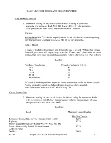
Best Thin-Film Research CellsStandard ConditionsBest Si and Concentrator Research CellsStandard ConditionsFig. 1. Evolution of research solar cell efficiencies over the lifetime of the DOE PV Technology Program. Upper figureshows thin-film technologies; lower figure shows Si and concentrators, comparing them to the thin films.2
been confirmed in this past period, and they are summarizedin Table 1. Amorphous Si:H, copper-indium-galliumdiselenide (CIGS), and cadmium telluride (CdTe) remainthe primary thin-film program technologies. The CIGStechnology continues to lead from a record-efficiency metric—and the 19.5% of this 4-µm-thick device is nearly thesame as its 250-µm-thick multicrystalline Si research counterpart. Thin-film CdTe (16.7% cell) continues to showmanufacturing progress, with large-area production-levelmodules measured above 10%.significantly beyond those anticipated for the current commercial PV approaches. However, crystalline Si researchremains a priority—because a rising host of improvementsand second-generation Si devices (e.g., thin and thin-film Si,innovative device designs, heterostructures) offer equallyimportant possibilities for the same economic targets. Newefforts in process research, process integration, and diagnostic development cultivate critical links between even themost fundamental studies and manufacturing in an entirelynew research approach aimed at cutting the time betweenlaboratory discovery or invention to industry introductionand use.The thin-film CIGS cell provides some insight into thevalue of the program and how effectively it functions tobring about technology advancement from a strong partnership among its industry / university / Laboratory components. The CIGS technology experienced a 60%–70% improvement from the 12% efficiency that it had reached inthe mid-1990s (see Fig. 1). How did this happen? Whatwas the research tipping point? It grew initially from Program or “motivational” influences that unleashed a chain ofscientific discoveries and understanding that guided improvements. First, there arose a real commercial interestand need (“context”), which was then augmented by theDOE Thin Film Partnership (“the few”). In parallel, a considerable foreign competition (“a few more”) provided bothan enhanced research base and a motivation for additionalfunding from the United States. In turn, these gave birth tocoordinated theory, modeling, deposition, and characterization projects that led to materials and device understandingand development. New areas of interface and materials engineering, defect analysis, development of special measurements—and the parallel advent of the nanotechnologyage—all provided pathways traceable to the science-basedimprovement of the technology. Every aspect of the devicewas meticulously investigated and optimized—from grainboundaries, to compositional gradients, to heterointerfaces,to window and transparent semiconductors, to contacts—nanoscale through macroscale, accounting for every photonand electron and hole within the structure. This investmentof persistent and coordinated financial and intellectual resources to the needs of the industry tipped this thin-filmtechnology to levels of performance beyond the expectations of the 1980s (“stickiness factor”). New physics, newunderstanding, and new methods provided the guidance forimprovement. This combination of the three agents ofchange defined by Gladwell—the Law of the Few, theStickiness Factor, and the Power of Context—tipped thismini-technical epidemic.The second area involves positioning the United States fortechnical leadership, decision-making, and ownership forthe host of next-technology options, including some thathave been called “third generation.” These options includethose with efficiencies (and perhaps principled on a different physics) beyond the conventional (ultra-high efficiencydevices such as “multi”-multijunctions, thermophotovoltaics/thermophotonics, intermediate bandgaps, quantumdots) and those with costs below current targets (ultra-lowcost approaches, including organics, quantum-layer and ultra-thin films, and biomimetics). Also, approaches that provide both electricity and chemical harvests (e.g., photoelectrochemical cells) can partner clean solar with clean fuelproduction.Performance (i.e., efficiency, reliability, durability) hasnot reached a limit. In fact, as we increase our understanding of these devices, we see that innovation, creativity, andtechnology advancement have continued to move the perceived “limits” to higher attainable levels. Figure 2 provides a glimpse of where the core program and enhancedR&D investments can take us for these technologies. We areat the tipping point to the next levels for many of these.Some suspend at the precipice to demonstrate technicalworth; others are at the brink of first-time commercial introduction. How effectively we make decisions and howquickly we reach our targets depend on many factors—butthe U.S. PV industry clearly defines a pathway that gives areal chance “to do things right.”3. ProgressThe 25-year advancement of the terrestrial PV technologies supported by DOE is represented in Fig. 1. Over thistimeframe, Si cells doubled and thin films more than tripledin efficiency. Multijunction devices have gone from concept to abandonment to reality—and now are approaching40% efficiency for terrestrial concentrator applications.New materials and novel approaches have been introducedwith technical promise not envisioned at the onset of theDOE Program. Excellent progress? Yes. The technologyworks well, and it is a real business. The final answer? No.Solar photovoltaics is real—now and for our future. It isboth the now and the future that we must take hold of.Crystalline Silicon. Some 94% of current world marketsales are for this PV product. Some have believed that because crystalline Si commands the market share, no furtherresearch is necessary! In fact, Si technology has continuedto advance, and several cell designs have been validatedwith efficiencies above 20%. Crystalline Si has been themain foundation of the DOE PVMaT and the PV Manufacturing R&D projects. Georgia Tech maintains the DOEUniversity Center of Excellence in silicon photovoltaics.The DOE-NREL Universities Program has focused onThin Films. The perennial bridesmaid of the PV technologies continues to show substantial progress. A sizeablenumber of headline research cells and record modules have3
Fig. 2. Representation of the performance-cost potential of the PV technologies under the current U.S. DOE funding expectations andthose proposed by the PV roadmap (shown as “Potential Roadmap”). The roadmap R&D and policy investments are expected to acceleratethe program by 10-20 years. (Evaluation by T. Surek and L.L. Kazmerski, 2004)Table 1. Recent headline performances for cell and module technologies supported under the U.S. DOE PV Subprogram. These representa set of these efficiency records confirmed during the past year.CellThin-film ZnO/CdS/CIGSThin-film CGSThin-film ZnO/CdS/CISThin-film ZnO/CIGS (no CdS)Thin-film CdTe (transparent)Thin-film CdTe-CIGS Tandem(mechanical stack)GaInP/GaAs/Ge MonolithicMultiple Junction Concentratora-Si:H/Floatzone Crystalline SiHeterojunctionModuleCdS/CdTeCdS/CIGS (on flexiblestainless steel)Efficiency(%)19.510.215.018.513.915.313.8 (CdTe)1.5 a2(cm 0.210.1Power(W)67.471.2Aperture Area(cm2)662470854Organization/Date/CommentsNREL (8/2004)NREL (4/2004)NREL (9/2004)NREL [5/2004)NREL (9/2004)NREL (11/2004) (13.8 top cell;1.5% bottom) Transparency oftop cell is 50%Boeing-Spectrolab (3/2004)Under 175.2x concentration (Isc .643 A; Pmax 1.724 W)NREL/Georgia Tech (9/2004)[“HIT”-type structure]Manufacturer/DateFirst Solar (2/2004)Global Solar/ITN (9/2004)(ITO/ZnO/CdS/CIGS/Mo/ss)
critical applied and fundamental research areas identified bythe U.S. industry. NREL has sponsored the annual Workshop on Crystalline Silicon for 14 years, which is a forumthat has brought together researchers from PV and the Sielectronics industry to exchange technical ideas and servesas the sounding board and provides guidance for researchneeds for PV technology. Growing from the most recentWorkshop, a “White Paper” is being formulated to guideDOE on crystalline Si research needs. Although these efforts have provided substantial contributions, the U.S. program lags behind the basic and applied efforts and investments currently under way in Europe and Japan. In response, the NCPV has recently established a new “Crystalline Silicon Program,” uniting the ensemble of resources inthe PV Technology Subprogram in a new partnership. TheNCPV has redirected some of its resources over the pastyear to build this area, responding to our industry’s guidance—both at the University Center of Excellence and in itsown internal R&D programs. Several significant contributions have already appeared. Collaborative work betweenNREL, Georgia Tech, and SunPower enhanced the understanding of the Si heterojunction (a-Si:H/crystalline Sicell)—reporting key aspects to achieve high efficiencies (theabrupt interface and uniform, thin a-Si:H layers), with a record cell efficiency confirmed. Initial work on realisticpaths to thin-film devices on glass substrates is under way.A revived activity aimed at supportive measurement andcharacterization techniques for Si technology has begun,including some activities aimed at meeting new and in-linediagnostics needs. However, all this must be expanded tohelp the industry close the performance gap between research cells and manufactured modules; to facilitate innovative manufacturing, processing, and in-line diagnostics development as part of the “manufacturing centers of excellence” called for in the industry roadmap; and to provide anR&D foundation for those next-generation Si technologiescited earlier. This is a priority for the NCPV and the DOEPV Subprogram.Certainly, the work on multijunction concentrators hasdrawn attention to the area of ultra-high efficiencies. TheBoeing/Spectrolab GaAsP/GaAs/Ge monolithic device currently leads with a verified efficiency of 37.3% (175.2xconcentration, 24.3 C, 0.264 cm2 area)—with similar research cells in Japan and Germany being a few efficiencypoints behind. Further optimization of this 3-junction structure is ongoing, but other approaches are under way. Adding a 1-eV GaInAsN junction to this successful 3-junctionstructure or the development of a lattice-mismatched monolithic cell hold promise to exceed 40% efficiency. The progress has been significant in this area with the added investment by the industry—and a 40%-efficienct researchconcentrating cell is likely before the current 39% 2007target [4]. Uniting the III-V semiconductors with Si has received some additional interest because of the success ofthese monolithic devices.Recently, a two-junctionGaAsNP/Si dual-junction cell was demonstrated (voltageaddition and tunnel junction). It is expected that improvednucleation of the III-V on the Si will provide another pathway toward an ultra-high efficiency concentrator based on aless expensive and higher efficiency Si bottom cell.The polycrystalline thin-film tandem-cell work covers avariety of activities and approaches. The target is a 25%cell, which could be attained, for example, by using a 1.7eV top-cell and a 1.1-eV bottom-cell partner (modeling predictions). The options include CdTe and alloys, CIS andvarious quaternaries, CuGaSe2, and Si. Monolithic and mechanical stacks are part of a critical-path research plan.Voltage addition has been demonstrated for several monolithic designs, with success of the pertinent interconnectjunction. Recently, a CdTe-CIGS 4-terminal tandem wasverified at 15.3% efficiency, using a specially developedtransparent 13.8%-CdTe top cell. Because of the accelerated work on the special top cell, an efficiency milestone forthis program was reached 9 months ahead of schedule.Such excellent progress in this and other tandems gives evidence that these technologies are approaching the criticalpoint of implementation—the position that will tip this toward prototype realization.High-Performance and Next-Generation PV. Exploring andevaluating options that could take PV to the next levels hasbeen at the foundation of U.S. PV research since the formation of the terrestrial program. From these options, many ofour current cells evolved from concept to the mainstream.These programs dealing with advanced and exploratoryR&D have been the “poster child” of the decision-makingprocess in the PV program—a reflection of the “stagegating” procedures we are now formalizing within the systems-driven process.Manufacturing R&D. Maintaining technology ownership isone of two major themes in the new U.S. PV IndustryRoadmap [1]. Support for centers of excellence, universities and national laboratories is called out as critical for this,and specifically for the “ Science and Technology Facilityat NREL to shorten by 50% the time between lab discoveries and industry use in manufacturing and products.” In thisand the previous roadmaps, attention to this manufacturingand processing R&D and to a “manufacturing center of excellence” are priorities—especially since the first major costreductions remain with the module itself [1]. The nationalprogram R&D serves part of this need—the internal research at the Labs and universities, as well as the major PVManufacturing R&D and Thin-Film Partnership Programs.These latter two programs remain as priorities and are providing a foundation for the center-of-excellence model. Thecenter-of-excellence concept is one that is key to supportingMuch of this R&D is designed to explore the ultimate performance limits of PV technologies. The “High Performance PV Project” was initiated in 2002, with the goal to“double the conversion efficiencies” of current technologies—aimed at thin-film multijunctions and pre-commercialconcentrators. Although slowed by under-support, somesignificant progress has been made based on the innovationand creativity of the partners in this effort, and thus helpingto give the United States early technical leadership.5
the industry in meeting the roadmap targets. This will encompass a consortium between industry, universities, andthe national laboratories, focusing on broad industry supportfor now and near-term manufacturing issues—as well as establishing mechanisms leading to adoption by or development of longer-term or advanced manufacturing. This center has to address Si and thin films, and needs direct industry input and oversight for its success. The focus should beon projects that provide broad industry support (solutionsthat can be pursued by a wide group of manufacturers).However, there should still be mechanisms to work on aproprietary basis for critical needs. The former, because ofthe general benefit produced, should be funded by the U.S.program as part of its support for its industry. The lattercould leverage funding from the companies themselves, ifnecessary. Because of the scope of manufacturing involved(i.e., processing, diagnostics, robotics, packaging, characterization, cells, modules, macroscale processes, nanoscaleprocesses), this may actually involve several operations atseveral pertinent organizations. Something that should notbe lost is that this program should also establish a mechanism to support graduate students to work specifically inthese areas of research. This activity is critical to “trainingour workforce,” which is especially important if the roadmap targets are even partially realized.industry leadership, realized by the best products worldwideat best costs—and the expansion of the U.S. markets.4. SummaryThe NCPV continues to lead and support the R&D priorities for the U.S. PV technology, in concert with its industry,university, and national laboratory partners. The programhas remained flexible and poised to respond to technologyneeds. The new “Crystalline Silicon Project” is such a response, along with some redirection of NREL internal research and some additional funding into the existing crystalline Si activity. So is the activity of the new Science andTechnology Facility in establishing the roadmap-identifiedpriority with a manufacturing science center of excellence.Thin-film R&D remains a priority.Progress based on world-leading science and technologyhas brought much of this R&D to its “tipping point,” at theverge of providing materials, processes, devices, and techniques to either adoption by the industry or to the realizationof new technologies. The new U.S. PV Industry Roadmaprecognizes the need for enhanced U.S. R&D investments ifwe are to tip and cross that threshold causing the flood ofsolar PV electricity to immerse our U.S. homes, businesses,grids, manufacturing, and federal facilities with this clean,secure power. Solar photovoltaics is real—now and for ourfuture.The new NREL Science and Technology Facility (S&TF)has been established specifically to meet many of these industry and R&D needs. A key component is the “processdevelopment and integration laboratory,” designed specifically to provide the direct interface with the industry fortheir needs. The facility itself is slated for initial operationsin mid-2006, but the design of the critical processintegration platforms is well under way. In addition, a real,working “industry/university advisory committee” has beenestablished to provide guidance and review of the activities—from conception to conclusion. The first scheduled“platform” will serve the crystalline silicon needs, with onefor the thin films scheduled thereafter. The platform provides a set of specifically designed and pertinent characterization tools, controlled-ambient automated sample handling,several materials and device processing systems common toindustry standards, and the facility and interface for an industry partner to “roll up” their own specialized equipmentto evaluate its capability (without having to interrupt thatmanufacturer’s own manufacturing lines). It is a “users facility” that brings the state-of-the-art diagnostics, control,analysis, and expertise to rub shoulders with the industryengineers to maximize transfer of information. Because thefacility is linked with the NREL materials, device, and characterization R&D laboratories, these capabilities and scientists/engineers will also interact with this new way of conducting the business of R&D. Additionally, the systemsdriven analysis tools will be incorporated to provide userswith real-time access and evaluation assistance. The ensemble of these facility designs and operations is part of thegoal to significantly reduce the time from laboratory discovery to industry adoption. This is a tipping point toward U.S.ACKNOWLEDGEMENTSThe author gratefully acknowledges the inputs and guidance from the researchers in the NCPV and its two University Centers of Excellence. He especially appreciates thehelp of Tom Surek, John Benner, Pete Sheldon, RommelNoufi, Sarah Kurtz, Dave Ginley, Mowafak Al-Jassim,Keith Emery, Martha Symko-Davies, Rick Mitchell, KenZweibel, Bob Birkmire, Ajeet Rohatgi, Susan Moon, IrenePassage, Al Hicks, & Don Gwinner. Finally, I want to acknowledge the support of the U.S. Department of Energyunder Contract DE-AC36-99G010337.REFERENCES[1] Our Solar Power Future: The U.S. Photovoltaics IndustryRoadmap Through 2030 and Beyond (SEIA, Washington, DC,2004).[2] Malcolm Gladwell, The Tipping Point (Back Bay [paperback edition], Boston, MA; 2002).[3] U.S. DOE Solar Energy Technologies Program Multi-YearTechnical Plan 2004–2007 (U.S. DOE, Washington, DC;2003). DOE/GO-102004-1775.[4] U.S. Department of Energy Photovoltaics Technology Plan2003–2007 (U.S. DOE, Washington, DC; 2003)SPECIAL RECOGNITIONSThe NCPV wants also to acknowledge and congratulate severalamong us who received special awards and honors during thisyear, including: Cecile Warner, ASES Solar Woman of the Year (June 2004) Timothy J. Coutts, IEEE PVSC Cherry Award (October 2004) Ajeet Rohatgi, NREL 2003 Rappaport Award (March 2004) Robert Annan, NREL 2004 Rappaport Award (November 2004) Bhushan Sopori, NCPV 2004 Rappaport Award (October 2004) Bhushan Sopori, US DOE Tech Transfer Award (March 2004) Global Solar/ITN and NREL, 2004 R&D 100 Award (November2004)6
Form ApprovedOMB No. 0704-0188REPORT DOCUMENTATION PAGEThe public reporting burden for this collection of information is estimated to average 1 hour per response, including the time for reviewing instructions, searching existing data sources,gathering and maintaining the data needed, and completing and reviewing the collection of information. Send comments regarding this burden estimate or any other aspect of thiscollection of information, including suggestions for reducing the burden, to Department of Defense, Executive Services and Communications Directorate (0704-0188). Respondentsshould be aware that notwithstanding any other provision of law, no person shall be subject to any penalty for failing to comply with a collection of information if it does not display acurrently valid OMB control number.PLEASE DO NOT RETURN YOUR FORM TO THE ABOVE ORGANIZATION.1. REPORT DATE (DD-MM-YYYY)2. REPORT TYPEJanuary 20054.3.DATES COVERED (From - To)Conference PaperTITLE AND SUBTITLE5a. CONTRACT NUMBERDE-AC36-99-GO10337Photovoltaics R&D: At the Tipping Point5b. GRANT NUMBER5c. PROGRAM ELEMENT NUMBER6.AUTHOR(S)5d. PROJECT NUMBERL.L. KazmerskiNREL/CP-520-375535e. TASK NUMBERPVC512015f. WORK UNIT NUMBER7.PERFORMING ORGANIZATION NAME(S) AND ADDRESS(ES)National Renewable Energy Laboratory1617 Cole Blvd.Golden, CO 80401-33939.8.PERFORMING ORGANIZATIONREPORT NUMBERNREL/CP-520-37553SPONSORING/MONITORING AGENCY NAME(S) AND ADDRESS(ES)10. SPONSOR/MONITOR'S ACRONYM(S)NREL11. SPONSORING/MONITORINGAGENCY REPORT NUMBER12. DISTRIBUTION AVAILABILITY STATEMENTNational Technical Information ServiceU.S. Department of Commerce5285 Port Royal RoadSpringfield, VA 2216113. SUPPLEMENTARY NOTES14. ABSTRACT (Maximum 200 Words)“ . . . with robust investments
at this "tipping point" for solar PV. 1. The Tipping Point In his recent best-selling book The Tipping Point, Mal-colm Gladwell scrutinized "that magic moment when an idea, trend, or social behavior crosses a threshold, tips, and spreads like wildfire" [2]. Our PV technology can be char-acterized by such tipping points during its .