Transcription
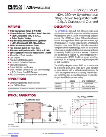
LT8606/LT8606B42V, 350mA SynchronousStep-Down Regulator with2.5µA Quiescent CurrentFEATURESnnnnnnnnnnnnnnnDESCRIPTIONWide Input Voltage Range: 3.0V to 42VUltralow Quiescent Current Burst Mode Operation:n 3µA I Regulating 12V to 3.3VQINOUTn Output Ripple 10mVP-PHigh Efficiency 2MHz Synchronous Operation:n 92% Efficiency at 0.35A, 12V to 5VINOUT350mA Maximum Continuous OutputFast Minimum Switch-On Time: 35nsAdjustable and Synchronizable: 200kHz to 2.2MHzSpread Spectrum Frequency Modulation for Low EMIAllows Use of Small InductorsLow DropoutPeak Current Mode OperationAccurate 1V Enable Pin ThresholdInternal CompensationOutput Soft-Start and TrackingSmall Thermally Enhanced 10-Lead MSOP Packageor 8-Pin 2mm 2mm DFN PackageAEC-Q100 Qualified for Automotive ApplicationsAPPLICATIONSnnGeneral Purpose Step-Down ConverterLow EMI Step DownAll registered trademarks and trademarks are the property of their respective owners.The LT 8606 is a compact, high efficiency, high speedsynchronous monolithic step-down switching regulatorthat consumes only 1.7µA of non-switching quiescentcurrent. The LT8606 can deliver 350mA of continuouscurrent. Low ripple Burst Mode operation enables highefficiency down to very low output currents while keepingthe output ripple below 10mVP-P. Internal compensationwith peak current mode topology allows the use of smallinductors and results in fast transient response and goodloop stability. The EN/UV pin has an accurate 1V thresholdand can be used to program VIN undervoltage lockout orto shut down the LT8606. The PG pin signals when VOUTis within 8.5% of the programmed output voltage as wellas fault conditions.The MSOP package includes a SYNC pin to synchronizeto an external clock, or to select Burst Mode operationor pulse-skipping with or without spread-spectrum; theTR/SS pin programs soft-start or tracking. The DFN package omits these pins and can be purchased in pulse-skipping or Burst Mode operation variety.PACKAGESYNC urst Mode OperationLT8606BDFNDFNPulse-Skipping ModeTYPICAL APPLICATION12VIN to 5VOUT Efficiency1005V, 2MHz Step-DownC21µFINTVCCC31µFC610nFfSW R GOODEFFICIENCY (%)VIN5.5V TO 42VL 10µH95 fSW 2MHz90858075706560C410µFX7R080555508606 TA01aL1 XFL3010-103ME050100150 200IOUT (mA)2503003508606 TA01bRev. DDocument FeedbackDownloaded from Arrow.com.For more information www.analog.com1
LT8606/LT8606BABSOLUTE MAXIMUM RATINGS(Note 1)VIN, EN/UV, PG.42VFB, TR/SS .4VSYNC Voltage .6VOperating Junction Temperature Range (Note 2)LT8606E. –40 C to 125 CLT8606I. –40 C to 125 CLT8606J. –40 C to 150 CLT8606H. –40 C to 150 CStorage Temperature Range. –65 C to 150 CPIN CONFIGURATIONTOP VIEWTOP VIEWBSTSWINTVCCRTSYNC1234511GND1098768 EN/UVBST 1EN/UVVINPGTR/SSFBSW 2INTVCC 39GNDRT 4MSE PACKAGE10-LEAD PLASTIC MSOP7 VIN6 PG5 FBDC PACKAGE8-LEAD (2mm 2mm) PLASTIC DFNθJA 40 C/WEXPOSED PAD (PIN 11) IS GND, MUST BE SOLDERED TO PCBθJA 102 C/WEXPOSED PAD (PIN 9) IS GND, MUST BE SOLDERED TO PCBORDER INFORMATIONLEAD FREE FINISHTAPE AND REELPART MARKING*PACKAGE DESCRIPTIONTEMPERATURE RANGELT8606EMSE#PBFLT8606EMSE#TRPBFLTGXT10-Lead Plastic MSOP–40 C to 125 CLT8606IMSE#PBFLT8606IMSE#TRPBFLTGXT10-Lead Plastic MSOP–40 C to 125 CLT8606HMSE#PBFLT8606HMSE#TRPBFLTGXT10-Lead Plastic MSOP–40 C to 150 CLT8606EDC#TRMPBFLT8606EDC#TRPBFLGXV8-Lead Plastic 2mm 2mm DFN–40 C to 125 CLT8606IDC#TRMPBFLT8606IDC#TRPBFLGXV8-Lead Plastic 2mm 2mm DFN–40 C to 125 CLT8606HDC#TRMPBFLT8606HDC#TRPBFLGXV8-Lead Plastic 2mm 2mm DFN–40 C to 150 CLT8606BEDC#TRMPBFLT8606BEDC#TRPBFLGXW8-Lead Plastic 2mm 2mm DFN–40 C to 125 CLT8606BIDC#TRMPBFLT8606BIDC#TRPBFLGXW8-Lead Plastic 2mm 2mm DFN–40 C to 125 CLT8606BHDC#TRMPBFLT8606BHDC#TRPBFLGXW8-Lead Plastic 2mm 2mm DFN–40 C to 150 CLT8606EMSE#WPBFLT8606EMSE#WTRPBFLTGXT10-Lead Plastic MSOP–40 C to 125 CLT8606IMSE#WPBFLT8606IMSE#WTRPBFLTGXT10-Lead Plastic MSOP–40 C to 125 CLT8606JMSE#WPBFLT8606JMSE#WTRPBFLTGXT10-Lead Plastic MSOP–40 C to 150 CLT8606HMSE#WPBFLT8606HMSE#WTRPBFLTGXT10-Lead Plastic MSOP–40 C to 150 CLT8606EDC#WTRMPBFLT8606EDC#WTRPBFLGXV8-Lead Plastic 2mm 2mm DFN–40 C to 125 CAUTOMOTIVE ead Plastic 2mm 2mm DFN–40 C to 125 CLT8606JDC#WTRMPBFLT8606JDC#WTRPBFLGXV8-Lead Plastic 2mm 2mm DFN–40 C to 150 CLT8606HDC#WTRMPBFLT8606HDC#WTRPBFLGXV8-Lead Plastic 2mm 2mm DFN–40 C to 150 CContact the factory for parts specified with wider operating temperature ranges. *The temperature grade is identified by a label on the shipping container.Tape and reel specifications. Some packages are available in 500 unit reels through designated sales channels with #TRMPBF suffix.**Versions of this part are available with controlled manufacturing to support the quality and reliability requirements of automotive applications. Thesemodels are designated with a #W suffix. Only the automotive grade products shown are available for use in automotive applications. Contact yourlocal Analog Devices account representative for specific product ordering information and to obtain the specific Automotive Reliability reports forthese models.2Downloaded from Arrow.com.Rev. DFor more information www.analog.com
LT8606/LT8606BELECTRICAL CHARACTERISTICSThe l denotes the specifications which apply over the full operatingtemperature range, otherwise specifications are at TA 25 C.PARAMETERCONDITIONSMINMinimum Input VoltageTYPMAX2.53.03.2VlVIN Quiescent CurrentUNITSVEN/UV 0VVEN/UV 2V, Not Switching, VSYNC 0V or LT8606 DFN, VIN 36Vl11.7512µAµAVIN Current in RegulationVIN 6V, VOUT 2.7V, Output Load 100µAVIN 6V, VOUT 2.7V, Output Load 1mAll5650090700µAµAFeedback Reference VoltageMSOP PackageVIN 6V, ILOAD 100mAVIN 6V, ILOAD 100mAl0.7740.7620.7780.7780.7820.798VVDFN PackageVIN 6V, ILOAD 100mAVIN 6V, ILOAD 100mAl0.7710.7530.7780.7780.7850.803VVFeedback Voltage Line RegulationVIN 4.0V to 40Vl 0.02 0.06%/VFeedback Pin Input CurrentVFB 1V 20nAMinimum On-TimeILOAD 300mA, SYNC 0V or LT8606 DFNILOAD 300mA, SYNC 1.9V or LT8606B DFNll35356560nsnsMinimum Off TimeILOAD 300mAl93130nsOscillator FrequencyMSOP PackageRT 221k, ILOAD 250mART 60.4k, ILOAD 250mART 18.2k, ILOAD 250mAlll1556401.902007002.002457602.10kHzkHzMHzDFN PackageRT 221k, ILOAD 250mART 60.4k, ILOAD 250mART 18.2k, ILOAD 250mAlll1406101.852007002.002607902.15kHzkHzMHzTop Power NMOS On-ResistanceILOAD 250mATop Power NMOS Current LimitMSOP Packagel0.653750.91.15ADFN Packagel0.651.11.4ABottom Power NMOS On-ResistancemΩ240SW Leakage CurrentVIN 36VEN/UV Pin ThresholdEN/UV RisingmΩ5l0.99EN/UV Pin Hysteresis1.051.1150EN/UV Pin CurrentVEN/UV 2VPG Upper Threshold Offset from VFBVFB Risingl5.0PG Lower Threshold Offset from VFBVFB Fallingl5.0PG HysteresisVPG 42VPG Pull-Down ResistanceVPG 0.1VSync Low Input VoltageMSOP OnlylSync High Input VoltageINTVCC 3.5V, MSOP Onlyl 20nA8.513.0%8.513.0%TR/SS Source CurrentMSOP OnlylTR/SS Pull-Down ResistanceFault Condition, TR/SS 0.1V, MSOP OnlySpread Spectrum Modulation FrequencyVSYNC 3.3V, MSOP Only5500.410.5VmV0.5PG LeakageµA% 200nA1200Ω0.9V2.73.2V23µA30090036ΩkHzRev. DFor more information www.analog.comDownloaded from Arrow.com.3
LT8606/LT8606BELECTRICAL CHARACTERISTICSNote 1: Stresses beyond those listed under Absolute Maximum Ratingsmay cause permanent damage to the device. Exposure to any AbsoluteMaximum Rating condition for extended periods may affect devicereliability and lifetime. Absolute Maximum Ratings are those values beyondwhich the life of a device may be impaired.Note 2: The LT8606E is guaranteed to meet performance specificationsfrom 0 C to 125 C junction temperature. Specifications over the –40 Cto 125 C operating junction temperature range are assured by design,characterization, and correlation with statistical process controls. TheLT8606I is guaranteed over the full –40 C to 125 C operating junctiontemperature range. The LT8606H is guaranteed over the full –40 C to150 C operating junction temperature range. High junction temperaturesdegrade operating lifetimes. Operating lifetime is derated at junctiontemperatures greater than 125 C.Note 3: This IC includes overtemperature protection that is intended toprotect the device during overload conditions. Junction temperature willexceed 150 C when overtemperature protection is active. Continuousoperation above the specified maximum operating junction temperaturewill reduce lifetime.TYPICAL PERFORMANCE CHARACTERISTICSEfficiency (5V Output,Burst Mode Operation)1009080EFFICIENCY (%)80757065VIN 12VVIN 24V557060504030050100150 200IOUT (mA)25030000.00135050403020VIN 12VVIN 24V104Downloaded from Arrow.com.1IOUT (mA)70650.11IOUT (mA)10VIN 12VVIN 24V50100 5000508606 G02100150 200IOUT (mA)2503003508606 G03Load Regulation0.200.15600.175FB Voltage700.018055780L 6.8µHfSW 2MHzSYNC 0V OR LT8606 DFN00.0010.018606 G01FB REGULATION VOLTAGE (mV)EFFICIENCY (%)808560VIN 12VVIN 24V10Efficiency (3.3V Output,Burst Mode Operation)90902060L 6.8µHfSW 2MHzSYNC 0V OR LT8606 DFN9510100 500779CHANGE IN VOUT (%)EFFICIENCY (%)85100L 10µHfSW 2MHzSYNC 0V OR LT8606 DFNEFFICIENCY (%)L 10µH95 fSW 2MHzSYNC 0V OR LT8606 DFN90100Efficiency (3.3V Output, BurstMode Operation)Efficiency (5V Output,Burst Mode Operation)10050TA 25 C, unless otherwise 5–50–103070110TEMPERATURE ( C)1508606 G058606 G04–0.20050100 150 200 250OUTPUT CURRENT (mA)3003508606 G06Rev. DFor more information www.analog.com
LT8606/LT8606BTYPICAL PERFORMANCE CHARACTERISTICSNo-Load Supply Currentvs Temperature (Not Switching)No-Load Supply Current(3.3V Output Switching)Line Regulation0.204.500.154.250.050.00–0.053.3L 10µHSYNC 0V OR LT8606 DFN3.14.002.93.752.7INPUT CURRENT (µA)0.10IIN (µA)CHANGE IN VOUT (%)TA 25 C, unless otherwise �0.152.251.5–0.202.002101826INPUT VOLTAGE (V)34422101826INPUT VOLTAGE (V)348606 G071.00TOP FET CURRENT LIMIT (A)TOP FET CURRENT LIMIT (A)1.100.900.800.70204060DUTY CYCLE (%)3070110TEMPERATURE ( C)1508606 G0980DUTY CYCLE 01.051.000.950.90–50100–103070110TEMPERATURE ( C)8606 G101508606 G11Switch Drop vs Temperature250–10Top FET Current Limitvs Temperature1.1001.3–508606 G08Top FET Current Limitvs Duty Cycle0.6042SYNC 0V OR LT8606 DFNSwitch Drop vs Switch Current200SWITCH CURRENT 350mA175SWITCH DROP (mV)SWITCH DROP (mV)20015010050TOP SWBOT SW0–50 –30 –10 10 30 50 70 90 110 130 150TEMPERATURE ( C)1501251007550TOP SWBOT SW2500508606 G12100 150 200 250SWITCH CURRENT (mA)3003508606 G13Rev. DFor more information www.analog.comDownloaded from Arrow.com.5
LT8606/LT8606BTYPICAL PERFORMANCE CHARACTERISTICSMinimum On-Timevs Temperature40Minimum Off-Timevs Temperature110IOUT 350mA39IOUT 300mA105MINIMUM OFF–TIME (ns)38MINIMUM ON–TIME (ns)TA 25 C, unless otherwise noted.3736353433321009590853130–50 –30 –10 10 30 50 70 90 110 130 150TEMPERATURE ( C)80–50 –30 –10 10 30 50 70 90 110 130 150TEMPERATURE ( C)8606 G148606 G15Switching Frequencyvs TemperatureDropout Voltage vs Output Current2025L XFL3010–682MERT 18.2kΩ2020200SWITCHING FREQUENCY (kHz)DROPOUT VOLTAGE .05 0.10 0.15 0.20 0.25 0.30 0.35OUTPUT CURRENT (A)1975–50–103070110TEMPERATURE ( C)8606 G168606 G17Minimum Load to Full Frequency(SYNC Float to 1.9V)(MSOP Package)Burst Frequency vs Output Current25002000OUTPUT CURRENT (mA)2250SWITCHING FREQUENCY (kHz)20L 6.8µHVIN 12VVOUT 3.3VSYNC 0V OR LT8606 DFN1750150012501000750500150L 10µHVIN 12VVOUT 5VRT 18.2kΩ1510525000255075100OUTPUT CURRENT (mA)1250058606 G186Downloaded from Arrow.com.1015 20 25 30 35INPUT VOLTAGE (V)40458606 G19Rev. DFor more information www.analog.com
LT8606/LT8606BTYPICAL PERFORMANCE CHARACTERISTICSSoft-Start Tracking(MSOP Package)Frequency Foldback25000.920000.817500.7FB VOLTAGE (V)FREQUENCY (kHz)1.0SYNC 0V OR LT8606 DFNRT 18.2kΩ2250TA 25 C, unless otherwise noted.1500125010007500.60.50.40.35000.22500.100.0 0.1 0.2 0.3 0.4 0.5 0.6 0.7 0.8 0.9 1.0FB VOLTAGE (V)000.1 0.2 0.4 0.5 0.6 0.7 0.8 1.0 1.1 1.2SS VOLTAGE (V)8606 G208606 G21Soft-Start Current vs Temperature(MSOP Package)2.53.25VIN UVLO2.33.002.2VIN UVLO (V)SOFT START CURRENT (µA)2.42.12.01.92.752.501.81.72.251.61.5–50 –30 –10 10 30 50 70 90 110 130 150TEMPERATURE ( C)2.00–50 –30 –10 10 30 50 70 90 110 130 150TEMPERATURE ( C)8606 G228606 G23Start-Up Dropout666555544443333222210VINVOUT012345INPUT VOLTAGE (V)67INPUT VOLTAGE (V)6RLOAD 50Ω11007RLOAD 15Ω1VINVOUT018606 G242345INPUT VOLTAGE (V)6OUTPUT VOLTAGE (V)7OUTPUT VOLTAGE (V)INPUT VOLTAGE (V)Start-Up Dropout77708606 G25Rev. DFor more information www.analog.comDownloaded from Arrow.com.7
LT8606/LT8606BTYPICAL PERFORMANCE CHARACTERISTICSSwitching WaveformsTA 25 C, unless otherwise noted.Switching WaveformsSwitching OAD100mA/DIVILOAD100mA/DIVILOAD100mA/DIV8606 G26200ns/DIV12VIN TO 5VOUT AT 250mA2MHz8606 G27200ns/DIV36VIN TO 5VOUT AT 250mA2MHzTransient Response2µs/DIV12VIN TO 5VOUT AT 5mA10µF COUT8606 G28Transient OAD100mA/DIV8606 G29200µs/DIVVIN 12V, VOUT 5V25mA TO 275mACOUT 22µFfSW 2MHz8606 G30200µs/DIVVIN 12V, VOUT 5V100mA TO 350mACOUT 22µFfSW 2MHzRadiated EMI Performance(CISPR25 Radiated Emission Test with Class 5 Peak Limits)50VERTICAL POLARIZATION45 PEAK DETECTOR40AMPLITUDE (dBµV)35302520151050CLASS 5 PEAK LIMITSPREAD SPECTRUM MODEFIXED FREQUENCY (MHz)DC2564A DEMO BOARDWITH EMI FILTER INSTALLED14V INPUT TO 5V OUTPUT AT 350mA, fSW 2MHz8Downloaded from Arrow.com.8606 G31Rev. DFor more information www.analog.com
LT8606/LT8606BPIN FUNCTIONSBST: This pin is used to provide a drive voltage, higherthan the input voltage, to the topside power switch. Placea 0.1µF boost capacitor as close as possible to the IC. Donot place a resistor in series with this pin.SW: The SW pin is the output of the internal powerswitches. Connect this pin to the inductor and boostcapacitor. This node should be kept small on the PCB forgood performance.INTVCC Internal 3.5V Regulator Bypass Pin. The internalpower drivers and control circuits are powered from thisvoltage. INTVCC max output current is 20mA. Voltageon INTVCC will vary between 2.8V and 3.5V. Decouplethis pin to power ground with at least a 1μF low ESRceramic capacitor. Do not load the INTVCC pin with external circuitry.RT: A resistor is tied between RT and ground to set theswitching frequency. When synchronizing, the RT resistorshould be chosen to set the LT8606 switching frequencyto equal or below the lowest synchronization input.SYNC (MSOP Only): External Clock Synchronization Input.Ground this pin for low ripple Burst Mode operation at lowoutput loads. Tie to a clock source for synchronizationto an external frequency. Leave floating for pulse-skipping mode with no spread spectrum modulation. Tie toINTVCC or tie to a voltage between 3.2V and 5.0V forpulse-skipping mode with spread spectrum modulation.When in pulse-skipping mode, the IQ regulating no loadwill increase to several mA. There is no SYNC pin on theLT8606 DFN package. The LT8606 DFN package internallyties SYNC to ground. The LT8606B package internallyfloats SYNC.FB: The LT8606 regulates the FB pin to 0.778V. Connectthe feedback resistor divider tap to this pin.TR/SS (MSOP Only): Output Tracking and Soft-Start Pin.This pin allows user control of output voltage ramp rateduring start-up. A TR/SS voltage below 0.778V forcesthe LT8606 to regulate the FB pin to equal the TR/SS pinvoltage. When TR/SS is above 0.778V, the tracking function is disabled and the internal reference resumes controlof the error amplifier. An internal 2μA pull-up current fromINTVCC on this pin allows a capacitor to program output voltage slew rate. This pin is pulled to ground with a300Ω MOSFET during shutdown and fault conditions; usea series resistor if driving from a low impedance output.There is no TR/SS pin on the LT8606 or LT8606B DFNand the node is internally floated.PG: The PG pin is the open-drain output of an internalcomparator. PG remains low until the FB pin is within 8.5% of the final regulation voltage, and there are nofault conditions. PG is valid when VIN is above 3.2V andwhen EN/UV is high. PG is pulled low when VIN is above3.2V and EN/UV is low. If VIN is near zero, PG will be highimpedance.VIN: The VIN pin supplies current to the LT8606 internalcircuitry and to the internal topside power switch. This pinmust be locally bypassed. Be sure to place the positiveterminal of the input capacitor as close as possible to theVIN pins, and the negative capacitor terminal as close aspossible to the GND pins.EN/UV: The LT8606 is shut down when this pin is lowand active when this pin is high. The hysteretic thresholdvoltage is 1.05V going up and 1.00V going down. Tieto VIN if the shutdown feature is not used. An externalresistor divider from VIN can be used to program a VINthreshold below which the LT8606 will shut down.GND: Exposed Pad Pin. The exposed pad must be connected to the negative terminal of the input capacitorand soldered to the PCB in order to lower the thermalresistance.Rev. DFor more information www.analog.comDownloaded from Arrow.com.9
LT8606/LT8606BBLOCK DIAGRAMVINVINCINR3OPT– INTERNAL 0.778V REFEN/UV1V –SHDNSLOPE COMPR4OPTPGERRORAMP 8.5%3.5VREG –INTVCCCVCCOSCILLATOR200kHz TO INTVCC UVLOVIN UVLOTR/SS (MSOP ONLY)2µASHDNTSDVIN TM2GNDRTSYNC (MSOP ONLY)8606 BD10Downloaded from Arrow.com.Rev. DFor more information www.analog.com
LT8606/LT8606BOPERATIONThe LT8606 is a monolithic constant frequency currentmode step-down DC/DC converter. An oscillator withfrequency set using a resistor on the RT pin turns onthe internal top power switch at the beginning of eachclock cycle. Current in the inductor then increases untilthe top switch current comparator trips and turns off thetop power switch. The peak inductor current at which thetop switch turns off is controlled by the voltage on theinternal VC node. The error amplifier servos the VC nodeby comparing the voltage on the VFB pin with an internal 0.778V reference. When the load current increasesit causes a reduction in the feedback voltage relative tothe reference leading the error amplifier to raise the VCvoltage until the average inductor current matches thenew load current. When the top power switch turns offthe synchronous power switch turns on until the nextclock cycle begins or inductor current falls to zero. If overload conditions result in excess current flowing throughthe bottom switch, the next clock cycle will be delayeduntil switch current returns to a safe level.If the EN/UV pin is low, the LT8606 is shut down anddraws 1µA from the input. When the EN/UV pin is above1.05V, the switching regulator becomes active.To optimize efficiency at light loads, the LT8606 entersBurst Mode operation during light load situations.Between bursts, all circuitry associated with controllingthe output switch is shut down, reducing the input supplycurrent to 1.7μA. In a typical application, 3.0μA will beconsumed from the input supply when regulating with noload. The SYNC pin is tied low to use Burst Mode operation and can be floated to use pulse-skipping mode. If aclock is applied to the SYNC pin the part will synchronizeto an external clock frequency and operate in pulse-skipping mode. While in pulse-skipping mode the oscillatoroperates continuously and positive SW transitions arealigned to the clock. During light loads, switch pulses areskipped to regulate the output and the quiescent currentwill be several mA. The SYNC pin may be tied high forspread spectrum modulation mode, and the LT8606 willoperate similar to pulse-skipping mode but vary the clockfrequency to reduce EMI. The LT8606 DFN has no SYNCpin and will always operate in Burst Mode operation. TheLT8606B has no SYNC pin and will operate in pulse-skipping mode.Comparators monitoring the FB pin voltage will pull the PGpin low if the output voltage varies more than 8.5% (typical) from the set point, or if a fault condition is present.The oscillator reduces the LT8606’s operating frequencywhen the voltage at the FB pin is low and the part is inBurst Mode operation. This frequency foldback helps tocontrol the inductor current when the output voltage islower than the programmed value which occurs duringstart-up.Rev. DFor more information www.analog.comDownloaded from Arrow.com.11
LT8606/LT8606BAPPLICATIONS INFORMATION2500Achieving Ultralow Quiescent CurrentAs the output load decreases, the frequency of single current pulses decreases (see Figure 1) and the percentageof time the LT8606 is in sleep mode increases, resulting in much higher light load efficiency than for typicalconverters. By maximizing the time between pulses, theconverter quiescent current approaches 3.0µA for a typical application when there is no output load. Therefore,to optimize the quiescent current performance at lightloads, the current in the feedback resistor divider mustbe minimized as it appears to the output as load current.While in Burst Mode operation the current limit of thetop switch is approximately 150mA resulting in outputvoltage ripple shown in Figure 3. Increasing the outputcapacitance will decrease the output ripple proportionally.As load ramps upward from zero the switching frequencywill increase but only up to the switching frequencyprogrammed by the resistor at the RT pin as shown inTable 1. The output load at which the LT8606 reaches theprogrammed frequency varies based on input voltage,output voltage, and inductor choice.For some applications it is desirable for the LT8606 to operate in pulse-skipping mode, offering two major differencesfrom Burst Mode operation. First is the clock stays awake atall times and all switching cycles are aligned to the clock. Inthis mode much of the internal circuitry is awake at all times,increasing quiescent current to several hundred µA. Secondis that full switching frequency is reached at lower outputload than in Burst Mode operation as shown in Figure 2. FullSwitching Frequency Minimum Load vs VIN in Pulse SkippingMode (MSOP ONLY). To enable pulse-skipping mode theSYNC pin is floated. To achieve spread spectrum modulation with pulse-skipping mode, the SYNC pin is tied high.Downloaded from Arrow.com.SWITCHING FREQUENCY T CURRENT (mA)1258606 F01Figure 1. SW Burst Mode Frequency vs Output Current20OUTPUT CURRENT (mA)To enhance efficiency at light loads, the LT8606 entersinto low ripple Burst Mode operation, which keeps theoutput capacitor charged to the desired output voltagewhile minimizing the input quiescent current and minimizing output voltage ripple. In Burst Mode operation theLT8606 delivers single small pulses of current to the output capacitor followed by sleep periods where the outputpower is supplied by the output capacitor. While in sleepmode the LT8606 consumes 1.7μA.12L 6.8µHVIN 12VVOUT 3.3VSYNC 0V2250L 10µHVIN 12VVOUT 5VRT 18.2kΩ151050051015 20 25 30 35INPUT VOLTAGE (V)40458606 F02Figure 2. Full Switching Frequency Minimum Load vs VIN inPulse Skipping Mode (MSOP 6 F03Figure 3. Burst Mode OperationWhile a clock is applied to the SYNC pin the LT8606 will alsooperate in pulse-skipping mode. The LT8606 DFN is alwaysprogrammed for Burst Mode operation and cannot enterpulse-skipping mode. The LT8606B DFN is programmed forpulse-skipping mode and cannot enter Burst Mode operation.Rev. DFor more information www.analog.com
LT8606/LT8606BAPPLICATIONS INFORMATIONFB Resistor NetworkOperating Frequency Selection and Trade-OffsThe output voltage is programmed with a resistor dividerbetween the output and the FB pin. Choose the resistorvalues according to:Selection of the operating frequency is a trade-off betweenefficiency, component size, and input voltage range. Theadvantage of high frequency operation is that smallerinductor and capacitor values may be used. The disadvantages are lower efficiency and a smaller input voltagerange. V R1 R2 OUT – 1 0.778V 1% resistors are recommended to maintain output voltageaccuracy.The total resistance of the FB resistor divider should beselected to be as large as possible when good low loadefficiency is desired: The resistor divider generates asmall load on the output, which should be minimized tooptimize the quiescent current at low loads.When using large FB resistors, a 10pF phase lead capacitor should be connected from VOUT to FB.Setting the Switching FrequencyThe LT8606 uses a constant frequency PWM architecture that can be programmed to switch from 200kHzto 2.2MHz by using a resistor tied from the RT pin toground. A table showing the necessary RT value for adesired switching frequency is in Table 1. When in spreadspectrum modulation mode, the frequency is modulatedupwards of the frequency set by RT.Table 1. SW Frequency vs RT ValuefSW (MHz)RT .60023.71.80020.52.00018.22.20016.2The highest switching frequency (fSW(MAX)) for a givenapplication can be calculated as follows:fSW(MAX) (VOUT VSW(BOT)t ON(MIN) VIN – VSW(TOP) VSW(BOT))where VIN is the typical input voltage, VOUT is the outputvoltage, VSW(TOP) and VSW(BOT) are the internal switchdrops ( 0.13V, 0.06V, respectively at max load) andtON(MIN) is the minimum top switch on-time (see ElectricalCharacteristics). This equation shows that slower switching frequency is necessary to accommodate a high VIN/VOUT ratio.For transient operation VIN may go as high as the Abs Maxrating regardless of the RT value, however the LT8606will reduce switching frequency as necessary to maintaincontrol of inductor current to assure safe operation.The LT8606 is capable of maximum duty cycle approaching 100%, and the VIN to VOUT dropout is limited by theRDS(ON) of the top switch. In this mode the LT8606 skipsswitch cycles, resulting in a lower switching frequencythan programmed by RT.For applications that cannot allow deviation from the programmed switching frequency at low VIN/VOUT ratios usethe following formula to set switching frequency:VIN(MIN) VOUT VSW(BOT)1– fSW t OFF(MIN)– VSW(BOT) VSW(TOP)where VIN(MIN) is the minimum input voltage withoutskipped cycles, VOUT is the output voltage, VSW(TOP) andVSW(BOT) are the internal switch drops ( 0.13V, 0.06V,respectively at max load), fSW is the switching frequency(set by RT), and tOFF(MIN) is the minimum switch offtime. Note that higher switching frequency will increasethe minimum input voltage below which cycles will bedropped to achieve higher duty cycle.Rev. DFor more information www.analog.comDownloaded from Arrow.com.13
LT8606/LT8606BAPPLICATIONS INFORMATIONInductor Selection and Maximum Output CurrentThe LT8606 is designed to minimize solution size byallowing the inductor to be chosen based on the outputload requirements of the application. During overload orshort circuit conditions the LT8606 safely tolerates operation with a saturated inductor through the use of a highspeed peak-current mode architecture.A good first choice for the inductor value is:L VOUT VSW(BOT)fSW 4where fSW is the switching frequency in MHz, VOUT isthe output voltage, VSW(BOT) is the bottom switch drop( 0.06V) and L is the inductor value in μH.To avoid overheating and poor efficiency, an inductormust be chosen with an RMS current rating that is greaterthan the maximum expected output load of the application. In addition, the saturation current (typically labeledISAT) rating of the inductor must be higher than the loadcurrent plus 1/2 of in inductor ripple current:1IL(PEAK) ILOAD(MAX) ΔL2where IL is the inductor ripple current as calculated several paragraphs below and ILOAD(MAX) is the maximumoutput load for a given application.As a quick example, an application requiring 0.25A outputshould use an inductor with an RMS rating of greaterthan 0.5A and an ISAT of greater than 0.7A. To keep theefficiency high, the series resistance (DCR) should be lessthan 0.04Ω, and the core material should be intended forhigh frequency applications.The LT8606 limits the peak switch current in order toprotect the switches and the system from overload faults.The top switch current limit (ILIM) is at least 0.65A atlow duty cycles and decreases linearly to at least 0.5Aat D 0.8. The inductor value must then be sufficient tosupply the desired maximum output current (IOUT(MAX)),which is a function of the switch current limit (ILIM) andthe ripple current:ΔIIOUT(MAX) ILIM – L214Downloaded from Arrow.com.The peak-to-peak ripple current in the inductor can becalculated as follows:ΔIL VOUT V1– OUT L fSW VIN(MAX) where fSW is the switching frequency of the LT8606, andL is the value of the inductor. Therefore, the maximumoutput current that the LT8606 will deliver depends onthe switch current limit, the inductor value, and the inputand output voltages. The inductor value may have to beincreased if the inductor ripple current does not allowsufficient maximum output current (IOUT(MAX)) given theswitching frequency, and maximum input voltage used inthe desired application.The optimum inductor for a given application may differfr
EN/UV Pin Current V EN/UV 2V 20 nA PG Upper Threshold Offset from V FB V FB Rising l 5.0 8.5 13.0 % PG Lower Threshold Offset from V FB V FB Falling l 5.0 8.5 13.0 % PG Hysteresis 0.5 % . 6A , 96% Efficiency, 3MHz Synchronous Silent Switcher 2 Step-Down DC/DC Converter with I Q 2.5µA V IN 3.4V to 42V , VOUT(MIN) 0.97V , IQ 2.5µA .


