Transcription
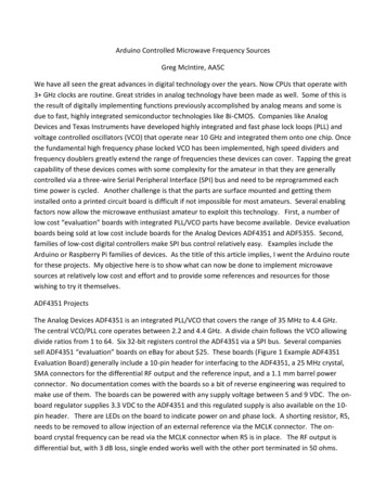
Arduino Controlled Microwave Frequency SourcesGreg McIntire, AA5CWe have all seen the great advances in digital technology over the years. Now CPUs that operate with3 GHz clocks are routine. Great strides in analog technology have been made as well. Some of this isthe result of digitally implementing functions previously accomplished by analog means and some isdue to fast, highly integrated semiconductor technologies like Bi-CMOS. Companies like AnalogDevices and Texas Instruments have developed highly integrated and fast phase lock loops (PLL) andvoltage controlled oscillators (VCO) that operate near 10 GHz and integrated them onto one chip. Oncethe fundamental high frequency phase locked VCO has been implemented, high speed dividers andfrequency doublers greatly extend the range of frequencies these devices can cover. Tapping the greatcapability of these devices comes with some complexity for the amateur in that they are generallycontrolled via a three-wire Serial Peripheral Interface (SPI) bus and need to be reprogrammed eachtime power is cycled. Another challenge is that the parts are surface mounted and getting theminstalled onto a printed circuit board is difficult if not impossible for most amateurs. Several enablingfactors now allow the microwave enthusiast amateur to exploit this technology. First, a number oflow cost “evaluation” boards with integrated PLL/VCO parts have become available. Device evaluationboards being sold at low cost include boards for the Analog Devices ADF4351 and ADF5355. Second,families of low-cost digital controllers make SPI bus control relatively easy. Examples include theArduino or Raspberry Pi families of devices. As the title of this article implies, I went the Arduino routefor these projects. My objective here is to show what can now be done to implement microwavesources at relatively low cost and effort and to provide some references and resources for thosewishing to try it themselves.ADF4351 ProjectsThe Analog Devices ADF4351 is an integrated PLL/VCO that covers the range of 35 MHz to 4.4 GHz.The central VCO/PLL core operates between 2.2 and 4.4 GHz. A divide chain follows the VCO allowingdivide ratios from 1 to 64. Six 32-bit registers control the ADF4351 via a SPI bus. Several companiessell ADF4351 “evaluation” boards on eBay for about 25. These boards (Figure 1 Example ADF4351Evaluation Board) generally include a 10-pin header for interfacing to the ADF4351, a 25 MHz crystal,SMA connectors for the differential RF output and the reference input, and a 1.1 mm barrel powerconnector. No documentation comes with the boards so a bit of reverse engineering was required tomake use of them. The boards can be powered with any supply voltage between 5 and 9 VDC. The onboard regulator supplies 3.3 VDC to the ADF4351 and this regulated supply is also available on the 10pin header. There are LEDs on the board to indicate power on and phase lock. A shorting resistor, R5,needs to be removed to allow injection of an external reference via the MCLK connector. The onboard crystal frequency can be read via the MCLK connector when R5 is in place. The RF output isdifferential but, with 3 dB loss, single ended works well with the other port terminated in 50 ohms.
For control of the boards I used an Arduino Uno. I had some experience with the Arduino Uno using itto control an Analog Devices AD9851 direct digital synthesizer (DDS) on the DDS-60 board usingsoftware Ross Keatinge, KT1F wrote. Ross wrote his code for the Arduino Really Bare Bones Board(RBBB) but it readily compiled and loaded on the Arduino Uno. Ross has made his software for theDDS-60 available at http://www.theladderline.com/node/10. Arduino is “an open source electronicsplatform based on easy-to-use hardware and software”. Arduino has a series of small, low-costcomputer boards. The Arduino Uno (Figure 2 Arduino Uno) is based on the Atmel ATMega328Pmicrocontroller.Figure 1 Example ADF4351 Evaluation Board
Figure 2 Arduino UnoThe Arduino Uno includes headers for a modest number of interface lines including six ADC inputs,digital lines programmable to be inputs or outputs, and important for these applications, SPI bus lines.The board can be powered either via the USB port or a 2.1 mm barrel connector. The USB port alsoserves for programming the ATMega328P.The Arduino Uno is popular as an educational tool and a number of “shields” have been developed forthe Arduino family of controllers. One popular shield (Figure 3 LCD Button Shield for Arduino)provides a 16 character by 2 line LCD, six push buttons, and connection points for soldering wires tointerface to the Arduino Uno. They are also available at low cost. The shields have header pins on theunderside allowing direct mounting to the header sockets on the Arduino Uno.
Figure 3 LCD Button Shield for ArduinoAn open-source integrated development environment (IDE) for the Arduino family of controllers isavailable at https://www.arduino.cc/en/Main/Software. Versions of the tool can be downloaded andused off-line on your computer or on-line. The tool allows you to write code for the Arduino boards,compile that code, and load it onto the board via a USB interface. Arduino code is like C code.Library functions are available for many common applications such as interfacing to an LCD display, akeypad, I2C devices, and again important for these applications, a SPI bus. Also of great utility is thatmany people have made their sketches, as programs for the Arduinos are known, available free online. Alain Fort, F1CJN wrote a sketch for the Arduino Uno to control the ADF4351 boards. This isavailable at http://f6kbf.free.fr/html/ADF4351%20and%20Arduino Fr Gb.htm. The web site alsocontains information on connecting the ADF4351 to the Arduino Uno via an LCD Button Shield. As hepoints out, it is important to include level shifters to interface the 5V logic of the Arduino Uno to the3.3V logic of the ADF4351.Integrating the Arduino Uno/Shield and the ADF4351 evaluation board/level shifter board results ina small two-part assembly (
Figure 5 ADF4351 Measured Spurious Performance at 3456 MHz). The example displayed on the LCD uses the on-board 25 MHz reference and is generating 2808 MHzwhich could be fed to an external frequency doubler for a 5616 MHz source. I use the 5V regulator onthe Arduino Uno to power the ADF4351 evaluation board. There is sufficient current capacity althoughI wouldn’t want to draw anymore from it as the regulator runs warm doing this. The unit can bepowered from a wall transformer and mounted on a chassis with standoffs to make a more permanentlab resource.The next question was what kind of spurious and phasenoise performance do these boards provide? Myexperience is that the data sheets are a good indicator ofthe performance you can expect but it will vary withoutput frequency, reference frequency, and referencequality among other things. Al Ward, W5LUA helpedmeasure spurious and phase noise for a range of LO andbeacon frequencies the microwave amateur might need.Spurious performance with the ADF4351 set to 3456 MHzand using the on-board 25 MHz crystal shows close-inperformance better than 50 dB (Figure 5 ADF4351Measured Spurious Performance at 3456 MHz). I did a
few spot checks later with a higher quality external 10 MHz reference and the spurs were generallyabout 10 dB lower. Phase noise performance was about -85 dBc at 10 KHz (Error! Reference source notfound.). Again, these measurements were taken with theFigure 4 Arduino Uno and ADF4351Evaluation Boardon-board 25 MHz crystal and a good reference improves performance. Depending on your application,you may want to add some downstream filtering. There are controls in the ADF4351 you can select tooptimize for best phase noise performance or best spurious performance as well as controls for manyother parameters. I have not yet tried to optimize the settings but there is likely room forimprovement.I measured output power of the ADF4351 evaluation board with this configuration of hardware andsoftware. It was easy to enter the different frequencies via the shield and collect the results (Figure 7ADF4351 Single-Ended Output Power vs. Frequency). Output power is programmable using two bits inregister 4 and can be programmed to a maximum value of 5 dBm in 3 dB steps. This value is for thedifferential power available using a balun on the output.
Figure 5 ADF4351 Measured Spurious Performance at 3456 MHzFigure 6 ADF4351 Phase Noise Performance at 3456 MHz
2Output Power (dBm)10-1010002000300040005000Output Power vsFrequency-2-3-4-5-6Frequency (MHz)Figure 7 ADF4351 Single-Ended Output Power vs. FrequencyFixed Frequency ApplicationsThe configuration described above is flexible, in terms of selecting an output frequency and one of tworeference frequencies. It is a useful lab resource. A simpler configuration is adequate for a fixedfrequency LO and I decided to trim both the hardware and software for this application. The LCDButton Shield is not necessary in this case so it was removed. On the Arduino Uno side, I soldered theinterface wires to header pins that plug into the header sockets. I continued to use socket pins withheat shrink on the end of the wire that plugs onto the header pin of ADF4351 evaluation board.The function of the Arduino Uno is to load the registers of the ADF4351 when power is applied.Software to handle the human interface (buttons and LCD display) is not needed. The register valuescan be entered into the front (definition) section of the sketch where variables and functions aredefined and then sent via the SPI bus just as in the F1CJN sketch. You can get the register values for aspecific output frequency and reference combination by either calculating them manually or by usingan Analog Devices downloadable tool available for use with their evaluation boards. The manualmethod is a good exercise to understand the math the PLL uses and the features and capability of thedevice while the tool is an expedient short cut. I calculated the register values for a number offrequency and reference combinations, entered them into the sketch, and then commented out all butthe one to be loaded. Other than a few lines of code in the setup section that call the SPI bus function
to load the registers, most of the code in the F1CJN sketch was stripped out. In fact, there are no linesof code in the loop section of the sketch I use for this application.I programmed an Arduino Uno for 3312 MHz and followed the ADF4351 with a MMIC amplifier to bringthe signal level up to the level needed by the mixer in my 3456 MHz transverter, 7 dBm. I trimmedthe MMIC amp output with a pad but this could probably be eliminated by programming a loweroutput power level in the ADF4351. The GaAs MMIC I used, a MGA82563, is powered directly from the3.3VDC available on the Arduino Uno. I used this combination to replace the 30 year old FrequencyWest “brick” in my 3456 MHz transverter. The ADF4351 is driven by the station 10 MHz reference thatdrives all my transverters. I calibrate it to a rubidium standard. On-the-air tests have been good andthere is good filtering in the transverter. It is certainly nice to eliminate or reduce the frequencyvariable in making long haul weak signal contacts.Beacon ApplicationA third ADF4351 project was the frequency source and keyer for a new 432.380 MHz beacon for theNorth Texas Microwave Society (NTMS). The hardware for this application is based on that describedabove for the fixed frequency application but includes the LCD Button shield. The LCD Button Shielddisplays the beacon ID and output frequency. Another addition is an LM34 temperature sensor. Thereal-time beacon power amplifier heat sink temperature is included in the beacon message. Thehardware (Figure 8 NTMS 432 MHz Beacon Block Diagram) includes a MAR-3 MMIC amplifier to drive asurplus Tech-Tron amplifier. RF output power of the beacon is just below 1W at the coax feed to theantenna.The software for this project started with the F1CJN ADF4351 software. I merged the code from a CWbeacon sketch developed by Mark VandeWettering, at-an-arduino-based-morse-beacon/comment-page1/). Keyer output is available on a digital line from the Arduino Uno. It quickly became apparent thatthe delays in the F1CJN human interface code were too long for the keyer code to operate properly so Istripped all the human interface code, save the LCD display, from the sketch.
Figure 8 NTMS 432 MHz Beacon Block DiagramThe original plan was to use the digital output from the Arduino Uno to key a PIN diode switch. Whenpresented at an NTMS meeting, the question as to whether the ADF4351 could be programmed to keythe output power directly was asked. Not too many more lines of code were required to toggle theoutput power enable of the ADF4351 in sync with the dots and dashes of the beacon message. Onthe-air tests have come back with T9 reports. Finally, I was asked if temperature could be included inthe beacon message as with the other NTMS beacons. I found an Arduino sketch for interfacing to anLM35 (Celsius) temperature sensor and adapted this for the Farenheight version, the LM34.The beacon is in the final construction stages. The plan is for it to go into full-time operation later thisyear following further testing and burn-in. The spectral tests already performed included the beaconfrequency and spurs which were down 60 dB using the on-board crystal. The final installation uses ahigh quality 10 MHz reference so this performance should improve and thus no filtering was deemednecessary.ADF5355Relatively inexpensive evaluation boards for the Analog Devices ADF5355 have also appeared on themarket. They are generally in the 75 range. Several versions have been available on eBay. Theversion I bought (Figure 9 Example ADF5355 Evaluation Board) has screw down terminals for inputpower, five SMA connectors, low drop-out regulators for 5VDC and 3.3VDC, a 16-pin header for I/O, a
26 MHz crystal, and five SMA connectors. Two LEDs are on the board to indicate power on and lock.Again, no documentation was provided so some reverse engineering was required.Figure 9 Example ADF5355 Evaluation BoardFirst, a 6VDC supply works well with the board. I use a 7806 regulator to feed it. Next, there are twoconnectors for the reference, A and B, or and -. The ADF5355 can take a differential reference input.A single-ended input works fine. Next, there are three output connectors. The ADF5355 covers therange of 54 MHz to 13.6 GHz. The VCO core runs from 3.4 GHz to 6.8 GHz. A 1 to 64 divider chainfollows the VCO as well as a doubler. Frequencies below 6.8 GHz are available at the differential RF Aoutputs while frequencies from 6.8 GHz to 13.6 GHz are available at the single-ended RF B output thatis fed by the frequency doubler. Finally, there are a number of solder bump jumpers on the board. TheJ8 jumper needs to be cleared to input an external reference. The on-board crystal output can besampled on the CLK A connector when the J8 jumper is in place. The J2 and J6 jumpers allow theregulated 5VDC and 3.3VDC to be available on the 16-pin header.The ADF5355 frequency range is much wider than the ADF4351. Also, the frequency resolution is veryfine. I calculated it to be 1 Hz or finer. This capability comes with some increased complexity. TheADF5355 has 13 32-bit registers that need to be programmed to control it. Part of this is due to theincreased width of the frequency control words. More on this below.The first thing I tried with an ADF5355 board was to load the registers with an Arduino Uno. I used thefixed frequency sketch from the ADF4351 projects and expanded the register set to 13. To get theregister values, I went through the frequency calculations and other parameter selections manually asan exercise to better understand the part. Analog Devices also has a tool for their ADF5355 evaluationboard that can be used to calculate the register values directly. The frequency values I calculated werethe same as the tool provided. There were a few other minor differences in parameters, e.g., charge
pump values, but the values I derived have worked well. Connecting the Arduino Uno to the ADF5355again required level shifters for the logic lines. Again, I used a small prototyping board to mount theADF5355 evaluation board and the level shifters. The first time I tried it, the ADF5355 came up andlocked to the 26 MHz on-board reference. I have built up fixed frequency stand-alone sources for5,616 MHz and 10, 224 MHz by selecting different register sets in the sketch and uploading them to therespective Arduino Uno. I removed the J8 solder jumper for these versions and feed an external 10MHz reference to the boards. Subsequently, I have replaced the old, venerable Frequency West“bricks” in my 5760 MHz and 10368 MHz transverters. Note that the ADF5355 parts run warm and Ihave experienced loss of lock when I didn’t allow the parts to access open air.The next project I tried was to apply the F1CJN software to get a dynamically programmable resourcefor the ADF5355 like for the ADF4351. Internet searches did not come up with any software like it forcontrolling the ADF5355. There are some low –cost frequency sources using the ADF5355 on eBay thatmust use something similar. I expanded the frequency calculations to address the more complicatedmath. Where an integer value with no remainder results, the answers were OK. However, when Ibegan calculating different values with a remainder, I quickly realized the limitations of an 8-bitprocessor for this demanding an application. I concluded that the Arduino Uno does not have theresolution needed to calculate the values for the ADF5355 and started working with an Arduino Due.The Arduino Due (Figure 10 Arduino Due) is a 32-bit board based on the Atmel AT91SAM3X8Eprocessor. It runs on an 84 MHz clock versus the Arduino Uno that runs on a 16 MHz clock. The I/O isexpanded significantly compared to the Arduino Uno. There are 12 ADCs that can provide higherresolution than on the Arduino Uno when programmed to do so and two DACs are included.Figure 10 Arduino Due
Two mini-USB ports are included, one for programming and another for devices like a mouse orkeyboard.Anyone who has ported code from one processor to another knows that it is not necessarily a simpletask. This case was no exception. Although I followed the concepts and structure of the F1CJNsoftware, I rewrote probably more than 75% of it. It might have been easier to start from scratch.Hardware-wise, the LCD Button Shield that fits on the Arduino Uno does fit and work on the ArduinoDue although great care needs to be taken as there are no keying features that would prevent onefrom installing it in the wrong place and damaging the Arduino Due or the LCD Button Shield or both.The first major problem I ran into when I tried compiling code Ihad run on the Arduino Uno for the Arduino Due was that theArduino Due, unlike the Arduino Uno, does not have any EEPROM.I wanted to be able to store output and reference frequencycombinations for easy retrieval. The solution was to add externalEEPROM. Small boards with the AT24C256 EEPROM are availablefor about 1 or so each (Figure 11 I2C EEPROM Boards).This EEPROM is 32K x 8 bits and has an I2C interface. I tapped 3.3Vpower and ground from the LCD button shield and connected theI2C lines to the second of two I2C interfaces (pins 21 and 22) onthe Arduino Due. Adding this hardware was the simple part.Figure 11 I2C EEPROM BoardsInterfacing the SPI bus on the ADF5355 evaluation board wassimpler in some respects and more complicated in others. The Arduino Due uses 3.3V I/O so theresistive level shifters were not required. The SPI bus, on the other hand, is on a separate 6-pin headerthat is just under one edge of the LCD Button Shield. The three lines needed on that connector can beaccessed with some creative bending of the socket pins used to connect them. The LE and MUXOUTlines are still mapped to the same I/O lines as on the Arduino Uno and accessible on the LCD ButtonShield. The resulting prototype hardware configuration (Figure 12 Arduino Due and ADF5355Evaluation Board Hardware) is a little awkward but should make a good lab asset when installed in achassis with everything secured. The prototyping board has a 7806 regulator run off 12 VDC. TheArduino Due, like the Arduino Uno, can be run from a 9 VDC wall transformer with a 2.1 mm plug.The software work included adding the code for the I2C EEPROM. There is an Arduino library functioncalled “wire” for interfacing to I2C devices. I wrote the code to pack and unpack the 32-bit words thatstore the frequency values and which of two references are to be used. Other major changes were thecode for calculating the divide ratio, selecting the correct RF output, and the calculations of the INT,
FRAC1, FRAC2, and MOD2 values needed by the ADF5355. This involved double precision arithmeticbut provided the resolution needed for the ADF5355. Other changes include the threshold values usedFigure 12 Arduino Due and ADF5355 Evaluation Board Hardwareto determine which button on the LCD Button Shield has been pressed. These values are different forthe Arduino Due versus the Arduino Uno. The fields on the LCD were expanded to cover the 10s ofGHz. Finally, the external EEPROM has more capacity than available on the Arduino Uno 8-bitprocessor so I expanded the number of frequency/reference combinations that can be stored to 100.ADF5355 PerformanceAgain Al Ward, W5LUA helped with the spectral and phase noise measurements, this time for theADF5355. The measurements presented here were made with the programmable version using theArduino Due as the controller and a good quality external 10 MHz reference.Output power and spectrum first. The spectral plot (Figure 13 ADF5355 Measured Spectrum at 10224MHz shows the carrier centered on 10224 MHz. The reference power level for the carrier is -12.3 dBm.The measured power output at the ADF5355 evaluation board was -8.5 dBm and the difference is thecable loss to the test equipment. The data sheet shows typical output power of -1 dBm at
Figure 13 ADF5355 Measured Spectrum at 10224 MHzFigure 14 ADF5355 Measured Phase Noise at 10224 MHz
13.6 GHz on RFout B. A second unit showed comparable output power. The difference between themeasured value and the data sheet may be due to evaluation board material although there is onlyone inch of trace from the chip to the output SMA on the board. A double check of the output powersetting in register 6 showed it being set to the maximum value. The spectrum is about as expected inthat the fundamental at 5112 MHz is about 10 dB down and the second harmonic at 15336 MHz isdown a bit over 40 dB. The noise floor, in this plot, is down about 60 dB.The phase noise (Figure 14 ADF5355 Measured Phase Noise at 10224 MHz shows the close-in phasenoise being about -70 dBc slowly dropping to about -75 dBc at 10 KHz. It drops rapidly from there. Al,W5LUA had phase noise plots of a 10224 MHz source based on the Apollo A32 board and a FrequencyWest “brick” oscillator and we compared them to the results for the ADF5355. The phase noiseperformance of the ADF5355 is similar to that measured for the A32-based source. The near-in phasenoise performance of the ADF5355 and the Frequency West “brick” are also similar. Further out, thephase noise of the Frequency West source rolls off much faster.Overall, this performance is pretty good, particularly for PLL-based technology. Use of a good imagefilter or other filter is recommended as with any doubler-based approach.SummaryMany details of the Analog Devices ADF4351 and ADF5355, and these projects, are not included heredue to space and time. I encourage interested readers to download the data sheets for the ADF4351and ADF5355 from the Analog Devices website. Analog Devices has many other highly integrated RFparts that are very interesting to study and work with. Likewise, Texas Instruments has some verypowerful devices like the LMX2594 which spans 10 MHz to 15 GHz. These devices also have greatperformance but I haven’t seen any low-cost evaluation boards for these devices to date. I alsoencourage interested readers to study the Arduino material available on the web and consider workingwith some of their boards. The IDE, large number of library functions, and long list of user-suppliedsketches make working with these controllers relatively simple and fun. The Raspberry PI familyshould work as well. I plan to further characterize performance and tinker with parameter settings aswell as a technology refresh for a set of transverters I built years ago for portable operation. I alsoplan to try some small heat sinks on the parts to improve thermal performance. I do not have a website but can make sketches available free for non-commercial amateur applications. Drop me an emailat AA5C@ARRL.Net and I will work each request on a case-by-case basis.
serves for programming the ATMega328P. The Arduino Uno is popular as an educational tool and a number of “shields” have been developed for the Arduino family of controllers. One popular shield (Figure 3 LCD Button Shield for Arduino) provides a 16 character by 2 line LCD, six p