Transcription
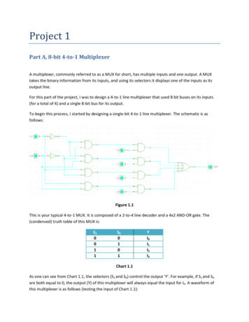
Project 1Part A, 8-bit 4-to-1 MultiplexerA multiplexer, commonly referred to as a MUX for short, has multiple inputs and one output. A MUXtakes the binary information from its inputs, and using its selectors it displays one of the inputs as itsoutput line.For this part of the project, I was to design a 4-to-1 line multiplexer that used 8 bit buses on its inputs(for a total of 4) and a single 8-bit bus for its output.To begin this process, I started by designing a single-bit 4-to-1 line multiplexer. The schematic is asfollows:Figure 1.1This is your typical 4-to-1 MUX. It is composed of a 2-to-4 line decoder and a 4x2 AND-OR gate. The(condensed) truth table of this MUX is:S10011S00101YI0I1I2I3Chart 1.1As one can see from Chart 1.1, the selectors (S1 and S0) control the output ‘Y’. For example, if S1 and S0are both equal to 0, the output (Y) of this multiplexer will always equal the input for I0. A waveform ofthis multiplexer is as follows (testing the input of Chart 1.1):
Figure 1.2
The next step was to extend this single-bit 4-to-1 line multiplexer to an 8-bit one. My final schematic isas follows:MUXMUXMUXMUXMUXMUXMUXMUXFigure 1.3I started off by producing 8 individual replicas of my single bit 4-to-1 line MUX (8 * 1 8 bits). I thencreated four 8-bit input pins. Each input pin was connected to a vertical expander. From there, eachindividual bit from a vertical expansion was connected to every individual 4-to-1 line MUX at thenecessary locations (every bit in i0 [has decimal digit ‘1’ for input in Figure 1.4] went into every firstposition [I0] of each MUX, every bit in i1 [has decimal digit ‘2’ for input in Figure 1.4] went into everysecond position [I1] of each MUX, etc ). There are 2 selectors, S1 and S0, that control the flow of datathroughout the circuit. Each selector is hooked up to every individual 4-to-1 line MUX at thecorresponding locations (S1 input goes to S1, etc ). The outputs of each multiplexer are attached to amerge bits controller which is connected to an 8-bit output pin. A waveform of this multiplexer is asfollows:
Figure 1.4I made each input a different value (I0 1, I1 2, I3 3, and I4 4). Using the selectors and testing theconditions in Chart 1.1, my waveform confirmed the results of a functional 4-to-1 line multiplexer.
Part B, 8-bit Full AdderA full adder takes 3 input bits, ‘A’, ‘B’, and ‘CIN’, performs binary addition, and outputs the results using2 bits, ‘OUT’ and ‘COUT’. ‘A’ and ‘B’ are the 2 values you wish to add. ‘CIN’ denotes a carry in bit. ‘OUT’represents the sum of ‘A’ and ‘B’, and ‘COUT’ is the carry out bit.For this project, I was to design an 8 bit-adder that had two 8-bit values as input and a single 8-bit valueproduced as a result.To begin this process, I started by designing a single-bit full adder. The schematic is as follows:Figure 1.5This is your typical full adder. It is composed of 2 XOR gates, 2 AND gates, and 1 OR gate. The truth tableof a full adder is as hart 1.2A waveform of my full adder is as follows (testing the inputs of Chart 1.2):OUT01101001
Figure 1.6The next step was to extend this single-bit full adder to an 8-bit one. My final schematic is as follows:Figure 1.7
I started off by producing 8 individual replicas of my single bit full adder (8 * 1 8 bits). I then createdtwo 8-bit input pins, one for ‘A’ and one for ‘B’. Each input pin was connected to a vertical expander.From there, each individual bit from a vertical expander was connected to every individual full adder atthe necessary locations (every bit in INPUT A went into every individual adder’s ‘A’ slot, every bit inINPUT B went into every individual adder’s ‘B’ slot). Each individual adder’s CIN was connected to theCOUT of the previous adder. A notable exception to this is the first and the last adders in the circuitdiagram. The first adder’s CIN was connected to a GND (ground) component that delivered a constantflow of ‘0’. Additionally, the last adder’s COUT was connected to a single-bit output pin called‘OVERFLOW’. The ‘OVERFLOW’ component was 0 for values A B 255. It is only when the sum of Aand B were greater than 255 that the component “turned on” denoting that a data overflow occurred.The maximum value for an 8 bit full adder to compute is 255 (28 256 [then subtract 1 from this resultto give 255 because of 0]). It, therefore, makes perfect sense that computing a sum larger than 255 willsignal the last adders ‘carry out’ value to equal ‘1’. To finalize my 8-bit full adder, I connected eachindividual single-bit adder’s output ‘OUT’ to a merge bits controller which is connected to an 8-bitoutput pin. A waveform of this circuit is as follows:Figure 1.8I knew that each individual single-bit full adder was functional due to my previous unit testing. Since an8-bit full adder is composed of eight single-bit full adders, I had only to test 3 other possibilities to provethat this circuit was working as intended. I chose a value less than 255, a value of 255, and a valuegreater than 255. These 3 choices allowed me to prove that all the single-bit adders worked correctly in
conjunction with one another and showed that my ‘OVERFLOW’ output pin was correctly identifying aproblem if one occurred.References"Adder (electronics)." Wikipedia, The Free Encyclopedia. Wikimedia, 15 Sep 2010. Web. 18 Sep 2010. http://en.wikipedia.org/wiki/Adder (electronics) .Mano, Morris, and Charles Kime. Logic and Computer Design Fundamentals. 4th. Upper Saddle River,New Jersey: Pearson Prentice Hall, 2008. 696. Print."Multiplexer." Wikipedia, The Free Encyclopedia. Wikimedia, 17 Sep 2010. Web. 19 Aug 2010. http://en.wikipedia.org/wiki/Multiplexer .
(for a total of 4) and a single 8-bit bus for its output. To begin this process, I started by designing a single-bit 4-to-1 line multiplexer. The schematic is as follows: Figure 1.1 This is your typical 4-to-1 MUX. It is composed of a 2-to-4 line decoder and a 4x2 AND-OR gate. The (condensed) truth