Transcription
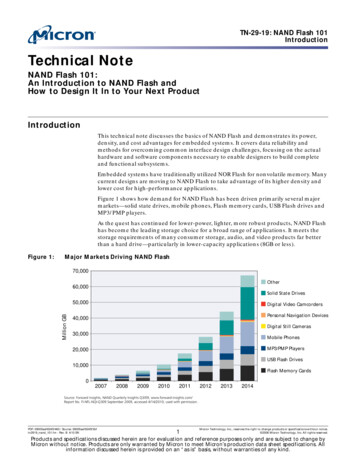
TN-29-19: NAND Flash 101IntroductionTechnical NoteNAND Flash 101:An Introduction to NAND Flash andHow to Design It In to Your Next ProductIntroductionThis technical note discusses the basics of NAND Flash and demonstrates its power,density, and cost advantages for embedded systems. It covers data reliability andmethods for overcoming common interface design challenges, focusing on the actualhardware and software components necessary to enable designers to build completeand functional subsystems.Embedded systems have traditionally utilized NOR Flash for nonvolatile memory. Manycurrent designs are moving to NAND Flash to take advantage of its higher density andlower cost for high-performance applications.Figure 1 shows how demand for NAND Flash has been driven primarily several majormarkets—solid state drives, mobile phones, Flash memory cards, USB Flash drives andMP3/PMP players.As the quest has continued for lower-power, lighter, more robust products, NAND Flashhas become the leading storage choice for a broad range of applications. It meets thestorage requirements of many consumer storage, audio, and video products far betterthan a hard drive—particularly in lower-capacity applications (8GB or less).Figure 1:Major Markets Driving NAND Flash70,000Other60,000Solid State DrivesMillion GB50,000Digital Video CamcordersPersonal Navigation Devices40,000Digital Still Cameras30,000Mobile PhonesMP3/PMP Players20,000USB Flash Drives10,000Flash Memory Cards020072008200920102011201220132014Source: Forward Insights, NAND Quarterly Insights Q3/09, www.forward-insights.com/Report No. FI-NFL-NQI-Q309 September 2009, accessed 4/14/2010; used with permission.PDF: 09005aef8245f460 / Source: 09005aef8245f3bftn2919 nand 101.fm - Rev. B 4/10 EN1Micron Technology, Inc., reserves the right to change products or specifications without notice. 2006 Micron Technology, Inc. All rights reserved.Products and specifications discussed herein are for evaluation and reference purposes only and are subject to change byMicron without notice. Products are only warranted by Micron to meet Micron’s production data sheet specifications. Allinformation discussed herein is provided on an “as is” basis, without warranties of any kind.
TN-29-19: NAND Flash 101Flash BasicsFlash BasicsThe NAND Flash device discussed in this technical note is based on a 2Gb asynchronousSLC device and its parameters (unless otherwise noted). Higher density devices andother more advanced NAND devices may have additional features and different parameters.The NAND Flash array is grouped into a series of blocks, which are the smallest erasableentities in a NAND Flash device.A NAND Flash block is 128KB. Erasing a block sets all bits to 1 (and all bytes to FFh).Programming is necessary to change erased bits from 1 to 0. The smallest entity that canbe programmed is a byte. Some NOR Flash memory can perform READ-While-WRITEoperations. Although NAND FLASH cannot perform READs and WRITEs simultaneously, it is possible to accomplish READ/WRITE operations at the system level using amethod called shadowing. Shadowing has been used on personal computers for manyyears to load the BIOS from the slower ROM into the higher-speed RAM.There is a limit to the number of times NAND Flash blocks can reliably be programmedand erased. Nominally, each NAND block will survive 100,000 PROGRAM/ERASE cycles.A technique known as wear leveling ensures that all physical blocks are exerciseduniformly. To maximize the life span of a design, it is critical to implement both wearleveling and bad-block management.Figure 2 shows a comparison of NAND Flash and NOR Flash cells. NAND efficiencies aredue in part to the small number of metal contacts in the NAND Flash string. NAND Flashcell size is much smaller than NOR Flash cell size—4F2 compared to 10F2—because NORFlash cells require a separate metal contact for each cell.PDF: 09005aef8245f460 / Source: 09005aef8245f3bftn2919 nand 101.fm - Rev. B 4/10 EN2Micron Technology, Inc., reserves the right to change products or specifications without notice. 2006 Micron Technology, Inc. All rights reserved.
TN-29-19: NAND Flash 101Flash BasicsFigure 2:Comparison of NAND and NOR Flash CellsNANDNORBit lineContactContactWord lineWord lineSource lineUnit CellSource line2F2FLayoutBit lineUnit CellBit lineCell Array5F2FCrossSectionCell Size4F210F2NAND Flash is very similar to a hard-disk drive. It is sector-based (page-based) and wellsuited for storage of sequential data such as pictures, video, audio, or PC data. Althoughrandom access can be accomplished at the system level by shadowing the data to RAM,doing so requires additional RAM storage. Also, like a hard-disk drive, a NAND Flashdevice may have bad blocks and requires error-correction code (ECC) to maintain dataintegrity.NAND Flash cells are 60% smaller than NOR Flash cells, providing the higher densitiesrequired for today’s low-cost consumer devices in a significantly reduced die area.NAND Flash is used in virtually all removable cards, including USB drives, secure digital(SD) cards, memory stick cards, CompactFlash cards, and multimedia cards (MMCs).The NAND Flash multiplexed interface provides a consistent pinout for all recentdevices and densities. This pinout allows designers to use lower densities and migrate tohigher densities without any hardware changes to the printed circuit board.PDF: 09005aef8245f460 / Source: 09005aef8245f3bftn2919 nand 101.fm - Rev. B 4/10 EN3Micron Technology, Inc., reserves the right to change products or specifications without notice. 2006 Micron Technology, Inc. All rights reserved.
TN-29-19: NAND Flash 101NAND vs. NOR ComparisonNAND vs. NOR ComparisonAdvantages of Each DeviceThere are specific advantages and disadvantages to using NAND Flash or NOR Flash inembedded systems (see Table 1). NAND Flash is best suited for file or sequential-dataapplications; NOR Flash is best suited for random access. Advantages of NAND Flashover NOR Flash include fast PROGRAM and ERASE operations. NOR Flash advantagesare its random-access and byte-write capabilities.Random access gives NOR Flash its execute-in-place (XiP) functionality, which is oftenrequired in embedded applications. An increasing number of processors include a directNAND Flash interface and can boot directly from the NAND Flash device (without NORFlash). These processors provide a very attractive solution when cost, space, and storagecapacity are important. Using these processors, XiP capability will cease to be a consideration when designing NAND Flash into embedded applications.Disadvantages of Each DeviceThe main NAND Flash disadvantage is slow random access; NOR Flash is hampered byslow WRITE and ERASE performance.Table 1:NAND Flash vs. NOR FlashNANDNORAdvantagesFast PROGRAMsFast ERASEsRandom accessByte PROGRAMs possibleDisadvantagesSlow random accessByte PROGRAMs difficultSlow PROGRAMsSlow ERASEsApplicationsFile (disk) applicationsVoice, data, video recorderReplacement of EPROMExecute directly from nonvolatilememoryAny large sequential dataRandom Access TimingRandom access time on NOR Flash is specified at 0.075µs; on NAND Flash, randomaccess time for the first byte only is significantly slower—25µs (see Table 2 on page 5).However, after initial access has been made, the remaining 2111 bytes are shifted out ofNAND at a mere 0.025µs per byte. This results in a bandwidth of more than 26 MB/s for8-bit I/Os and 41 MB/s for 16-bit I/Os.PDF: 09005aef8245f460 / Source: 09005aef8245f3bftn2919 nand 101.fm - Rev. B 4/10 EN4Micron Technology, Inc., reserves the right to change products or specifications without notice. 2006 Micron Technology, Inc. All rights reserved.
TN-29-19: NAND Flash 101NAND vs. NOR ComparisonTable 2:NAND/NOR CharacteristicsCharacteristicRandom access READSustained READ speed(sector basis)Random WRITE speedSustained WRITE speed(sector basis)Erase block sizeERASE time per block (TYP)NAND Flash: MT29F2G08ANOR Flash: TE28F128J325µs (first byte)0.025µs each for remaining 2111 bytes26 MB/s (x8) or 41 MB/s (x16)0.075µs 220µs/2112 bytes7.5 MB/s31 MB/s (x8) or62 MB/s (x16)128µs/32 bytes0.250 MB/s128KB500µs128KB1 secNAND Flash Design BenefitsThe real benefits of NAND Flash are faster PROGRAM and ERASE times, as NAND Flashdelivers sustained WRITE performance exceeding 7 MB/s. Block erase times are animpressive 500µs for NAND Flash compared with 1 second for NOR Flash. Clearly,NAND Flash offers several compelling advantages. The one challenge is that it is notwell-suited for direct random access. As noted previously, this can be handled with codeshadowing.Structural DifferencesNAND Flash offers several structural advantages over NOR Flash, starting with the pincount. The hardware pin requirements for NAND Flash and NOR Flash interfaces differmarkedly. NOR Flash requires approximately 44 I/O pins for a 16-bit device, while NANDFlash requires only 24 pins for a comparable interface (see Table 3). The multiplexedcommand, address, and data bus reduces the number of required pins by nearly 45%. Anadded benefit of the multiplexed interface is that higher-density NAND Flash devicescan be supported using the same hardware design and printed circuit board (PCB) usedfor lower densities. The common TSOP-1 package has been in use for many years, andthis feature enables customers to migrate to higher-density NAND Flash devices usingthe same PCB design.Another advantage of NAND Flash is evident in the packaging options. For example, thisNAND Flash device offers a monolithic 2Gb die or it can support up to four stacked die,accommodating an 8Gb device in the same package. This makes it possible for a singlepackage and interface to support higher densities in the future.Table 3:Required Hardware PinsNAND Flash: 23 Pins (x16)NOR Flash: 44 PinsI/O device-type interface, composed of:Random-access interface, typically composed [23:0]WP#Chip enableWrite enableRead enableCommand latch enableAddress latch enableData bus (I/O[15:0} for x16 parts)Write protectReady/busyPDF: 09005aef8245f460 / Source: 09005aef8245f3bftn2919 nand 101.fm - Rev. B 4/10 EN5Chip enableWrite enableOutput enableData busAddress busWrite protectMicron Technology, Inc., reserves the right to change products or specifications without notice. 2006 Micron Technology, Inc. All rights reserved.
TN-29-19: NAND Flash 101NAND Flash Architecture and Basic SLC OperationNAND Flash Architecture and Basic SLC OperationThe 2Gb NAND Flash device is organized as 2048 blocks, with 64 pages per block (seeFigure 3). Each page is 2112 bytes, consisting of a 2048-byte data area and a 64-bytespare area. The spare area is typically used for ECC, wear-leveling, and other softwareoverhead functions, although it is physically the same as the rest of the page. ManyNAND Flash devices are offered with either an 8- or a 16-bit interface. Host data isconnected to the NAND Flash memory via an 8-bit- or 16-bit-wide bidirectional databus. For 16-bit devices, commands and addresses use the lower 8 bits (7:0). The upper 8bits of the 16-bit data bus are used only during data-transfer cycles.Figure 3:2Gb NAND Flash Device Organized as 2048 BlocksSerial input (x8 or x16):25ns (MAX CLK)2112 bytesPROGRAM: 220µs/page64NAND Flash Memory ArrayNAND Flash Page 2112 bytes64 pagesper blockSerial output (x8 or x16):25ns (MAX CLK)Register64READ (page load): 25µsBLOCK ERASE: 500µs2048 blocks (2Gb SLC device)NAND Flash Block8-bit byteor 16-bit wordData area: 2048 bytesSpare area(ECC, etc.)64 bytesErasing a block requires approximately 500µs. After the data is loaded in the register,programming a page requires approximately 220µs. A PAGE READ operation requiresapproximately 25µs, during which the page is accessed from the array and loaded intothe 16,896-bit (2112-byte) register. The register is then available for the user to clock outthe data.In addition to the I/O bus, the NAND Flash interface consists of six major control signals(see Table 4 on page 7). (Note: The # symbol after a signal indicates that the signal isasserted LOW.)PDF: 09005aef8245f460 / Source: 09005aef8245f3bftn2919 nand 101.fm - Rev. B 4/10 EN6Micron Technology, Inc., reserves the right to change products or specifications without notice. 2006 Micron Technology, Inc. All rights reserved.
TN-29-19: NAND Flash 101NAND Flash Architecture and Basic SLC OperationTable 4:Signal tionAddress latch enableWhen ALE is HIGH, addresses are latched into the NANDFlash address register on the rising edge of the WE#signal.Chip enableIf CE is not asserted, the NAND Flash device remains instandby mode and does not respond to any controlsignals.Command latch enable When CLE is HIGH, commands are latched into theNAND Flash command register on the rising edge of theWE# signal.Ready/busy#If the NAND Flash device is busy with an ERASE,PROGRAM, or READ operation, the R/B# signal isasserted LOW. The R/B# signal is open drain andrequires a pull-up resistor.Read enableRE# enables the output data buffers.Write enableWE# is responsible for clocking data, address, orcommands into the NAND Flash device.Data is shifted into or out of the NAND Flash register 8 or 16 bits at a time. In aPROGRAM operation, the data to be programmed is clocked into the data register on therising edge of WE#. Special commands are used to randomly access data or move dataaround within the register to make random access possible; see “RANDOM DATA INPUTOperation” on page 15 and “READ FOR INTERNAL DATA MOVE Operation” on page 20.Data is output from the data register in a similar fashion by means of the read enable(RE#) signal, which is responsible for outputting the current data and incrementing tothe next location. The WE# and RE# clocks can run as fast as 25ns per transfer. When RE#or chip enable (CE#) are not asserted LOW, the output buffers are tri-stated. This combination of CE# and RE# activates the output buffers, enabling NAND Flash to share thedata bus with other types of memory, such as NOR Flash, SRAM, or DRAM. This featureis sometimes referred to as “chip enable don’t care.” The primary purpose of this reference is to differentiate very old NAND Flash devices, which require CE# to be assertedfor the entire cycle.All NAND Flash operations are initiated by issuing a command cycle. This is accomplished by placing the command on I/O[7:0], driving CE# LOW and CLE HIGH, thenissuing a WE# clock. Commands, addresses, and data are clocked into the NAND Flashdevice on the rising edge of WE# (see Figure 4 and Table 5 on page 8).Most commands require a number of address cycles followed by a second commandcycle. With the exception of the RESET and READ STATUS commands, new commandsshould not be issued when the device is busy (see Figure 4 and Table 5 on page 8).PDF: 09005aef8245f460 / Source: 09005aef8245f3bftn2919 nand 101.fm - Rev. B 4/10 EN7Micron Technology, Inc., reserves the right to change products or specifications without notice. 2006 Micron Technology, Inc. All rights reserved.
TN-29-19: NAND Flash 101NAND Flash Architecture and Basic SLC OperationFigure 4:Command Cycles for NAND Flash OperationsCLECE#RE#ALEtRR/B#WE#I/Ox00hCommandcycle 1Address (5 cycles)30hAddress cyclesCommandcycle 2tCEACE#tREARE#I/OxDOUTDon't CareTable 5:Command Cycles and Address CyclesCommandREAD PAGEREAD PAGE CACHE SEQUENTIALREAD PAGE CACHE SEQUENTIAL LASTREAD for INTERNAL DATA MOVERANDOM DATA READREAD IDREAD STATUSPROGRAM PAGEPROGRAM PAGE CACHEPROGRAM for INTERNAL DATA MOVERANDOM DATA INPUTERASE BLOCKRESETPDF: 09005aef8245f460 / Source: 09005aef8245f3bftn2919 nand 101.fm - Rev. B 4/10 ENCommandCycle 1Number ofAddressCyclesData CyclesRequired1CommandCycle NoNoNoNoNoNoYesNoNoNoNoNoYes8Micron Technology, Inc., reserves the right to change products or specifications without notice. 2006 Micron Technology, Inc. All rights reserved.
TN-29-19: NAND Flash 101NAND Flash CommandsThe addressing scheme for a 2Gb NAND Flash device is shown in Table 6. The first andsecond address cycles (or bytes) specify the column address, which specifies the startingbyte within the page. The last column location is 2112, so the address of this last locationis 08h in the second byte, and 3Fh in the first byte. PA[5:0] specify the page addresswithin the block, and BA[16:6] specify the block address. While the full 5-byte address isrequired for most PROGRAM and READ operations, only the first and second bytes (orcycles) are required for operations that access data randomly within the page. TheBLOCK ERASE operation requires only the three most significant bytes (third, fourth,and fifth) to select the block.Table 6:2Gb SLC NAND Flash Addressing otes:1. Block address concatenated with page address actual page address. CAx columnaddress; PAx page address; BAx block address. The page address and the block address,collectively, constitute the row address.2. If CA11 1, then CA[10:6] must be 0.3. The most significant address byte is the fifth cycle; the least significant address byte is thefirst cycleNAND Flash CommandsWhen any NAND Flash command is issued, CE# and ALE must be LOW, CLE must beasserted, and write clocks (WE#) must be provided. When any NAND Flash address isissued, CE# and CLE must be LOW, ALE must be asserted, and write clocks (WE#) mustbe provided. While the device is busy, only two commands can be issued: RESET andREAD STATUS.RESET OperationThe simplest NAND Flash command is the RESET (FFh) command (see Figure 5). TheRESET command does not require an address or subsequent cycle(s) (see Table 5 onpage 8). Simply assert CLE and issue a write clock with FFh on the data bus, and a RESEToperation is performed. This RESET command must be issued immediately followingpower-up, and prior to issuing any other command.RESET is one of two commands that can be issued while the NAND Flash device is busy(see Table 5 on page 8). If the device is busy processing a previous command, issuing aRESET command aborts the previous operation. If the previous operation was an ERASEor PROGRAM command, issuing a RESET command aborts the command prematurely,and the desired operation does not complete. ERASE and PROGRAM can be timeconsuming operations; issuing the RESET command makes it possible to abort eitherand reissue the command at a later time.PDF: 09005aef8245f460 / Source: 09005aef8245f3bftn2919 nand 101.fm - Rev. B 4/10 EN9Micron Technology, Inc., reserves the right to change products or specifications without notice. 2006 Micron Technology, Inc. All rights reserved.
TN-29-19: NAND Flash 101NAND Flash CommandsFigure 5:RESET CommandCLECE#tWBWE#tRSTR/B#I/OxFFhRESET commandREAD ID OperationThe READ ID (90h) command requires one dummy address cycle (00h), but it does notrequire a second command cycle (see Table 5 on page 8). After the command anddummy addresses are issued, the ID data can be read out by keeping CLE and ALE LOWand toggling the RE# signal for each byte of ID. Figure 6 shows the timing of the READ IDoperation, and Table 7 shows the format of the 5-byte response.Figure 6:READ ID CommandCLECE#WE#tARALERE#tWHRI/Ox90h00htREAByte 0Byte 1Byte 2Byte 3Byte 4Address, 1 cyclePDF: 09005aef8245f460 / Source: 09005aef8245f3bftn2919 nand 101.fm - Rev. B 4/10 EN10Micron Technology, Inc., reserves the right to change products or specifications without notice. 2006 Micron Technology, Inc. All rights reserved.
TN-29-19: NAND Flash 101NAND Flash CommandsTable 7:READ ID on001011002Ch2Gb, x8, 3V2Gb, x8, 3V2Gb, x8, 1.8V2Gb, x16, 00b00b01bOptionByte 0 – Manufacturer IDManufacturerByte 1 – Device Byte 2Number of die per CE#Cell typeNumber of simultaneouslyprogrammed pagesInterleaved operationsbetween multiple dieCache programmingByte value1SLC1000Not 11100001b80hByte 3Page sizeSpare area size (bytes)Block size (w/o spare)OrganizationSerial access (MIN)Serial access (MIN)Byte valueByte 000000111101b1b01b0b1b1xxxb0xxx0b95hD5h15h55hByte 4ReservedPlanes per CE#Plane sizeReservedByte value12GbMT29F2GxxNotes:PDF: 09005aef8245f460 / Source: 09005aef8245f3bftn2919 nand 101.fm - Rev. B 4/10 EN00101101000000b00b101b0b50h1. b binary; h hexadecimal11Micron Technology, Inc., reserves the right to change products or specifications without notice. 2006 Micron Technology, Inc. All rights reserved.
TN-29-19: NAND Flash 101NAND Flash CommandsTable 8:READ ID Parameters for Address otes:1. h hexadecimalREAD STATUS OperationREAD STATUS (70h) is the second command that can be issued while the NAND Flashdevice is busy. This command does not require an address or second command cycle.The status of the NAND Flash device can be monitored by issuing the RE# clock signalfollowing the READ STATUS command. If the READ STATUS command is used tomonitor the ready state of the device, the command should be issued only one time, andthe status can be re-read by re-issuing the RE# clock. Alternatively, the RE# signal can bekept LOW, waiting to receive the appropriate status bit before proceeding. READ STATUSalso reports the status of the write-protect signal, and the pass/fail status of previousPROGRAM or ERASE operations. It is mandatory that the pass status be attained onPROGRAM or ERASE operations to ensure proper data integrity.Table 9:READ STATUS ResponseSR BitPROGRAMPAGEPROGRAMPAGE CACHEMODE0Pass/failPass/fail (N)––1–Pass/fail (N - yReady/busy7Write protectReady/busycache2Write protectReady/busycache2Write protect[15:8]––Notes:PDF: 09005aef8245f460 / Source: 09005aef8245f3bftn2919 nand 101.fm - Rev. B 4/10 ENPAGE READPAGE READ CACHE l0 Successful PROGRAM/ERASE1 Error in PROGRAM/ERASE–0 Successful PROGRAM/ERASE1 Error in PROGRAM/ERASE–0–0–0Ready/busy 0 Busy1 ReadyReady/busy 0 Busy1 ReadyWrite0 Protectedprotect1 Not protected–01. Status register bit 5 is 0 during the actual programming operation. If cache mode is used,this bit will be 1 when all internal operations are complete.2. Status register bit 6 is 1 when the cache is ready to accept new data. R/B# follows bit 6.12Micron Technology, Inc., reserves the right to change products or specifications without notice. 2006 Micron Technology, Inc. All rights reserved.
TN-29-19: NAND Flash 101NAND Flash CommandsERASE OperationThe BLOCK ERASE (60h) operation erases an entire block of 64 pages, or 128KB total. Toissue a BLOCK ERASE operation, use the WE# signal to clock in the ERASE (60h)command with CLE asserted. Next, clock in three address cycles, keeping ALE assertedfor each byte of address. (These three address cycles are the most significant addresscycles and include the block address and the page address, as shown in Table 6 onpage 9.) The page address portion (the six low-order bits of the third address cycle) isignored, and only the block address portion of the three most significant bytes is used.After the address is input completely, issue the second command (command cycle 2) ofD0h, which is clocked in with WE# while CLE is being asserted. This confirms the ERASEoperation, and the device goes busy for approximately 500µs. When the devicecompletes this operation, it is ready for another command. The READ STATUScommand can be issued at any time, even when the device is busy during the ERASEoperation. The microprocessor or controller can monitor the device via the READSTATUS command.Figure 7:ERASE CommandCLECE#WE#ALEtBERSR/B#RE#I/Ox60hAddress input (3 cycles)70hD0hI/O5 0 BusyI/O5 1 ReadyDon‘t CarePDF: 09005aef8245f460 / Source: 09005aef8245f3bftn2919 nand 101.fm - Rev. B 4/10 EN13Micron Technology, Inc., reserves the right to change products or specifications without notice. 2006 Micron Technology, Inc. All rights reserved.
TN-29-19: NAND Flash 101NAND Flash CommandsPROGRAM OperationsPROGRAM operations can only program bits to 0 and assume that the user started with apreviously erased block.If the user does not want to program a bit (or group of bits), the bits can be kept in theerased state by setting that particular bit/group to 1.When the PROGRAM PAGE (80h) command is received, the input register is reset (internally) to all 1s. This supports inputting only bytes of data that are to be programmedwith 0 bits. The PROGRAM operation starts with the 80h command (with CLE asserted—see Figure 8). Next, de-assert CLE and assert ALE to input the full five address cycles.After the command and address are input, data is input to the register. When all the datahas been input, the 10h command is issued to confirm the previous command and startthe programming operation.A PROGRAM operation typically requires 220µs, although it may require as much as600µs. It is mandatory that the user read the status and check for successful operation. Ifthe operation is not successful, the block should be logged as a bad block and not usedin the future. All data should be moved to a good block.Figure 8:PROGRAM CommandCLECE#tWCtADLWE#tWBtPROGALERE#I/Ox80hColadd 1SERIAL DATAINPUT commandColadd 2Rowadd 1Rowadd 2Rowadd 3DINDINNM1 up to m bytesserial input10h70hPROGRAMcommandREAD STATUScommandStatusR/B#x8 device: m 2112 bytesx16 device: m 1056 wordsPDF: 09005aef8245f460 / Source: 09005aef8245f3bftn2919 nand 101.fm - Rev. B 4/10 EN14Don‘t CareMicron Technology, Inc., reserves the right to change products or specifications without notice. 2006 Micron Technology, Inc. All rights reserved.
TN-29-19: NAND Flash 101NAND Flash CommandsRANDOM DATA INPUT OperationAs the boxed area in Figure 9 shows, the RANDOM DATA INPUT (85h) commandrequires only 2 bytes of address followed by the data. This command is used foraccessing data randomly within a page—for example, to access ECC data. RANDOMDATA INPUT can be used to jump to the end of the page and write the ECC data. Theuser can input as many address and data combinations as desired. It is only after the 10hcommand is issued that the data is actually programmed to the selected page.Figure 9:PROGRAM Command with Random Data olRow Row Rowadd 1 add 2 add 1 add 2 add 3DINNDINN 1Serial inputSERIALDATA INPUTcommand85hColadd 1Coladd 2RANDOM Column addressDATA INPUTcommandDINNDINN 1Serial input10hPROGRAMcommandStatus70hREAD STATUScommandR/B#Random data input sequenceDon‘t CarePartial-Page ProgrammingDue to the large size of NAND Flash pages, partial-page programming is useful forstoring smaller amounts of data. Each NAND Flash page can accommodate four PCsized, 512-byte sectors. The spare area of each page provides additional storage for ECCand other software information.While it is advantageous to write all four sectors at once, often this is not possible. Forexample, when data is appended to a file, the file might start out as 512 bytes, then growto 1024 bytes. In this situation, a second PROGRAM PAGE operation is required to writethe second 512 bytes to the NAND Flash device. The maximum number of times a partialpage can be programmed before an ERASE is required is four. Note that for MLC devices,only one partial-page PROGRAM per page is supported between ERASE operations.PDF: 09005aef8245f460 / Source: 09005aef8245f3bftn2919 nand 101.fm - Rev. B 4/10 EN15Micron Technology, Inc., reserves the right to change products or specifications without notice. 2006 Micron Technology, Inc. All rights reserved.
TN-29-19: NAND Flash 101NAND Flash CommandsStorage MethodsThe two common methods for storing data and spare information in the same page areshown in Figure 10. The first method shows a data area of 512 bytes plus the 16-bytespare area directly adjacent to it; 528 bytes for the combined areas. A 2112-byte page cancontain four of these 528-byte elements. The second implementation involves storingthe data and spare information separately. The four 512-byte data areas are stored first,and their corresponding 16-byte spare areas follow, in order, at the end of the page.Figure 10:Typical Storage MethodsAdjacent Data and Spare Areas2112 bytesData area 1(512 bytes)Spare area 1(16 bytes)Data area 2(512 bytes)Spare area 2(16 bytes)Data area 3(512 bytes)Spare area 3(16 bytes)Data area 4(512 bytes)Spare area 4(16 bytes)Separate Data and Spare Areas2048 bytesData area 1(512 bytes)Data area 2(512 bytes)Data area 3(512 bytes)64 bytesData area 4(512 bytes)Spare areas1, 2, 3, 4READ OperationA READ operation starts with the 00h command, followed by five address cycles, thenthe 30h command to confirm the command sequence (see Figure 11). After the READtransfer time (tR) of approximately 25µs has elapsed, the data is loaded into the registerand ready for output. Asserting RE# enables the NAND Flash device to output the firstbyte of data corresponding to the column address specified in the address. SubsequentRE# transitions output data from successive column locations. When the RE# signal isHIGH (not asserted), the I/O lines are tri-stated. Reading past the end of the device (byte2112 or word 1056) results in invalid data.PDF: 09005aef8245f460 / Source: 09005aef8245f3bftn2919 nand 101.fm - Rev. B 4/10 EN16Micron Technology, Inc., reserves the right to change products or specif
connected to the NAND Flash memory via an 8-bit- or 16-bit-wide bidirectional data bus. For 16-bit devices, commands and addres ses use the lower 8 bits (7:0). The upper 8 bits of the 16-bit data bus are used only during data-transfer cycles. Figure 3: 2Gb NAND Flash Device Organized as