Transcription
Mid-IR and UV-Vis-NIR Mueller matrix ellipsometry characterization of tunablehyperbolic metamaterials based on self-assembled carbon nanotubesStefan Schöche, Po-Hsun Ho, John A. Roberts, Shangjie J. Yu, Jonathan A. Fan, and Abram L. FalkCitation: Journal of Vacuum Science & Technology B 38, 014015 (2020); doi: 10.1116/1.5130888View online: https://doi.org/10.1116/1.5130888View Table of Contents: https://avs.scitation.org/toc/jvb/38/1Published by the American Vacuum SocietyARTICLES YOU MAY BE INTERESTED INImaging ellipsometry for curved surfacesJournal of Vacuum Science & Technology B 38, 014016 (2020); https://doi.org/10.1116/1.5129654Spectral ellipsometry of monolayer transition metal dichalcogenides: Analysis of excitonic peaks in dispersionJournal of Vacuum Science & Technology B 38, 014002 (2020); https://doi.org/10.1116/1.5122683Ultrasensitive broadband infrared 4 4 Mueller-matrix ellipsometry for studies of depolarizing and anisotropic thinfilmsJournal of Vacuum Science & Technology B 38, 014003 (2020); https://doi.org/10.1116/1.5129800In situ real-time and ex situ spectroscopic analysis of Al2O3 films prepared by plasma enhanced atomic layerdepositionJournal of Vacuum Science & Technology B 38, 014014 (2020); https://doi.org/10.1116/1.5122797Plasmonic coupling and how standard ellipsometry can feel surface plasmonJournal of Vacuum Science & Technology B 38, 013603 (2020); https://doi.org/10.1116/1.5122267Brilliant mid-infrared ellipsometry and polarimetry of thin films: Toward laboratory applications with laser basedtechniquesJournal of Vacuum Science & Technology B 37, 060801 (2019); https://doi.org/10.1116/1.5122869
ARTICLEavs.scitation.org/journal/jvbMid-IR and UV-Vis-NIR Mueller matrix ellipsometrycharacterization of tunable hyperbolic metamaterialsbased on self-assembled carbon nanotubesCite as: J. Vac. Sci. Technol. B 38, 014015 (2020); doi: 10.1116/1.5130888Submitted: 7 October 2019 · Accepted: 27 December 2019 ·Published Online: 16 January 2020Stefan Schöche,1 Po-Hsun Ho,2 John A. Roberts,2 Shangjie J. Yu,2 Jonathan A. Fan,2View OnlineExport CitationCrossMarkand Abram L. Falk3AFFILIATIONS1J.A. Woollam Co., Inc., 645 M St., Suite 102, Lincoln, Nebraska 685082Stanford University, 348 Via Pueblo, Spilker Building, Room 307, Stanford, California 94305-4088IBM T.J. Watson Research Center, 1101 Kitchawan Road, Yorktown Heights, New York 105983Note: This paper is part of the Conference Collection: 8th International Conference on Spectroscopic Ellipsometry 2019, ICSE.ABSTRACTMueller matrix ellipsometry over the wide spectral range from the mid-IR to UV is applied to characterize the dielectric function tensor forfilms of densely packed single-walled carbon nanotubes aligned in the surface plane. These films optically act as metamaterials with anin-plane anisotropic, bulk effective medium response. A parameterized oscillator model is developed to describe electronic interbandtransitions, π π w plasmon resonances, and free-carrier absorption. Wide ranges of hyperbolic dispersion are observed and exceptionaltuneability of the hyperbolic ranges is demonstrated by comparing results for a film of aligned but unordered carbon nanotubes with a filmfabricated under optimized conditions to achieve hexagonally close-packed alignment of the nanotubes. The effect of doping on the opticalproperties and hyperbolic range is discussed.Published under license by AVS. https://doi.org/10.1116/1.5130888I. INTRODUCTIONHyperbolic metamaterials (HMM) were proposed as amultifunctional platform to realize waveguiding, imaging, sensing,and quantum and thermal engineering beyond conventional deviceperformance.1 HMMs display hyperbolic (or indefinite) dispersion,which originates from one of the principal components of theirelectric or magnetic effective tensor having the opposite sign to theother two principal components. Type-I HMMs have one negativecomponent of the dielectric tensor (εzz , 0; εxx , εyy . 0), whileType-II HMMs have two negative components (εxx , εyy , 0;εzz . 0). Traditionally, HMMs are formed by combining a metallicand dielectric building block, either as thin sheets (Type-II) ormetal nanorods embedded in a dielectric matrix (Type-I).2However, these materials have fixed hyperbolic spectral ranges andare not dynamically tunable.In this paper, we demonstrate a novel approach to form Type-IHMMs based on carbon nanotubes (CNTs). The one-dimensionalcharacter of electrons, phonons, and excitons in individual singlewalled CNTs leads to extremely anisotropic electronic, thermal,and optical properties. Recently, the preparation of large-scaleJ. Vac. Sci. Technol. B 38(1) Jan/Feb 2020; doi: 10.1116/1.5130888Published under license by AVS.monodomain films of aligned single-walled CNT using slowvacuum filtration was demonstrated.3 A refinement of this technique showed that nanotubes in these films can be aligned andcrystallized into two-dimensional ordered arrays with domainsizes of approximately 25 nm.4 Control of the doping level andvarious grating methods lead to highly tunable optical properties.We recently demonstrated that densely packed CNT films optically act as a metamaterial with an in-plane anisotropic, bulkeffective medium response.5 Hyperbolic modes confined in nanoribbon resonators with differing widths and orientations relativeto the nanotube were shown to support strong light localization.In order to predict and tune the optical behavior of these nanoribbon resonators, the hyperbolic spectral ranges in the dielectricfunction tensor of bulk CNT films need to be determined.Early publications reported intrinsic uniaxial behavior inCNTs aligned within the surface plane.6,7 The Maxwell-Garnetteffective medium approximation utilizing the dielectric functiontensor components of graphite proved to be insufficient to correctlydescribe the experimentally observed dielectric function tensorcomponent perpendicular to the CNT axes. A similar discrepancy38, 014015-1
ARTICLEwas found when applying effective medium approximations to thevertically aligned CNT (Ref. 8) and randomly oriented bundles ofCNTs.9 Early theoretical studies confirmed that effective mediumtheories will work to some extent in films containing isolatedCNTs but fail to correctly describe densely packed films due toneglect of the effect of the diameter-dependent curvature in theCNT and the interaction between densely packed nanotubes.10,11Detailed calculations considering the geometry of the CNT basedon k p theory,12,13 tight-binding models,14,15 or density functionaltheory16,17 successfully described the optical response of CNT filmsand confirmed that the optical response parallel and perpendicularto the CNT axes must be described independently. The diameterand helical arrangement of the CNT were predicted to stronglyinfluence the electronic character and observed optical absorption.Armchair CNTs were demonstrated to show metallic behavior,while zigzag and chiral nanotubes are semiconducting.16 In bothcases, discrete valence and conduction band levels are formedwith the distance between the highest valence band and thelowest conduction band level being higher in metallic CNTs thantheir semiconducting counterparts. Besides the interband transitions, a strong and broad π π w plasmon absorption is expectedin the ultraviolet (UV) spectral range, which slightly shifts for different polarization directions.16 Further, the conductivity inmetallic and doped semiconducting CNTs will be observed asfree-carrier absorption in the infrared spectral range. Muchhigher conductivity is observed along the CNT axes compared tothe perpendicular direction.18The polarization dependence of the interband transitions, thefree-carrier absorption, and the π π w plasmon, as well as theirchange with alignment, doping, and packing density of the nanotubes, determines the ranges of hyperbolic behavior in the dielectricfunction tensor in bulk effective mediums formed from the alignedCNT. The strongest optical anisotropy can be expected when allCNTs are aligned in one direction, resulting in effective uniaxialoptical properties with the optical axis along the CNT axes and theordinary dielectric function tensor component perpendicular to theCNT axes.19 The determination of the entire anisotropic dielectricfunction tensor requires advanced optical characterization techniques and measurement geometries. The polarization dependenceof interband transitions in the aligned CNT has been studied inlimited spectral ranges using polarized transmission,20 polarizedreflection,21 and polarized photoluminesence.22 Standard spectroscopic ellipsometry measurements were performed on horizontallybut randomly aligned CNTs with in-plane isotropic opticalproperties.18,23–27 In this geometry, the anisotropy of the bulk effective medium is reduced due to averaging over all CNTs within thesurface plane and only the tensor component perpendicular to thenanotube axes is uniquely defined. However, there is limited sensitivity to this so-called out-of-plane component of the dielectricfunction tensor (along the surface normal) in a reflection or transmission measurement even at oblique incidence and particularly inregions with absorption.28In this article, we describe the unambiguous determination ofthe uniaxial dielectric function tensor of bulk effective mediumsformed from the aligned CNT. A multisample, multi-angle-ofincidence, and multiazimuth approach using Mueller matrix spectroscopic ellipsometry over the wide spectral range from theJ. Vac. Sci. Technol. B 38(1) Jan/Feb 2020; doi: 10.1116/1.5130888Published under license by AVS.avs.scitation.org/journal/jvbmid-IR to the NIR-Vis-UV is applied to characterize the freecarrier, interband transitions, and π π w -plasmon resonancerelated features perpendicular and along the CNT axes. Regions ofhyperbolic dispersion are identified in the obtained dielectricfunction tensor and their shift with packing density and doping ofthe CNT films is discussed.II. EXPERIMENTThe CNT films in this work were fabricated by the vacuumfiltration method.3,5 A powder of arc-discharge single-walled CNTswith an average diameter of 1.41 nm was dispersed in water with thesurfactant sodium dodecylbenzenesulfonate. The CNTs were notsorted and the solution contained approximately 1/3 metallic and 2/3semiconducting CNT of an average length of 500 nm. A very weakvacuum then slowly pulled the suspension through a polycarbonatemembrane causing the nanotubes to self-organize and align in theplane of the membrane. The membrane was then dried, and theone-inch-in-diameter CNT films were transferred to a silicon substrate. The filtration membranes for the vacuum filtration process(Whatman Nuclepore tracketched polycarbonate hydrophilic membranes, 0.05 μm pore size) were first treated with a 2 Torr air plasmafor 30 s. This treatment provides a negative-charge surface on themembrane, which proved to be an important step for achieving ahigh degree of nanotube alignment and high packing density. Twodifferent kinds of films were produced for this study: one of alignedbut unordered CNTs and the other of aligned and ordered, i.e.,hexagonally close-packed (“crystallized”) CNTs. The crystallinityof the CNT films was demonstrated before by means of transmission electron microscopy and x-ray diffraction.4 To study theoptical properties in dependence of doping, we identify three distinct doping conditions. CNT films exposed to ambient conditions for an extended period of time (“ambient-doped”) areknown to be unintentionally doped by adsorbates (e.g., water)resulting in small p-type conductivity.29,30 Minimally doped conditions are achievable by vacuum annealing.4 To induce strongp-type surface-charge-transfer doping, the crystallized film wasexposed to HNO3 vapor for 10 min. The doping level wears offslowly during exposure to atmospheric conditions. The ellipsometry measurements on the doped CNT film were performed about24 h after the initial doping step when moderate doping levels stillremain in the sample. A cross section transmission electronmicroscopy image and a top-view scanning electron microscopyimage of the crystallized film are shown in Fig. 1.Mueller matrix spectroscopic ellipsometry measurementsat several angles of incidence and for a large number of sampleazimuth orientations were obtained on a NIR-Vis-UV ellipsometer(J.A. Woollam Co. RC2 with an automated rotation stage, 193–1690 nm) and combined in a multisample analysis with dataacquired on a mid-IR ellipsometer (J.A. Woollam Co. IR-VASEMark II, 1.4–35 μm) at several angles of incidence and for measurement direction along, perpendicular, and 45 rotated with respectto the CNT axes. The NIR-Vis-UV ellipsometer is equipped withtwo rotating compensators and can access the entire Muellermatrix. Access to the full Mueller matrix allows for the calculationof the depolarization index,31 which was found to be .0.98 overthe entire measured spectral range, indicating that depolarization38, 014015-2
ARTICLEFIG. 1. Cross section transmission electron microscopy image (a) and top-viewscanning electron microscopy image (b) for the crystallized film of single-walledCNTs. The hexagonal order and alignment direction are indicated by thesketches in the pictures.effects minimally influence the measurements on the CNT filmsstudied here. The mid-IR ellipsometer utilizes a single rotatingcompensator on the detector side and can access the first threecolumns of the Mueller matrix. Due to symmetry properties of theMueller matrix and considering that depolarization can be neglectedas indicated by the measurements on the NIR-Vis-UV ellipsometer,this is sufficient to fully characterize the anisotropic dielectric function tensor of the CNT films studied here. All datasets were combined and analyzed simultaneously using one optical model.III. THEORYWe are determining the dielectric function tensor of ourCNT films by spectroscopic ellipsometry in a reflection mode.For isotropic samples and uniaxial samples with the optical axisalong the surface normal, no mode conversion for p-polarized light(within the plane of incidence) to s-polarized light ( perpendicularto the plane of incidence) and vice versa occurs upon reflection,and the so-called standard ellipsometry formalism can be applied.32In our case, all nanotubes and thus the optical axis of our bulk effective mediums are aligned parallel to the surface plane. Whenever theoptical axis is not perfectly aligned parallel or perpendicular tothe plane of incidence, mode conversion of s-polarized light top-polarized light and vice versa occurs, and the so-called generalizedellipsometry formalism has to be applied.32 Here, either the entireJones matrix must be measured (if the sample is nondepolarizing) orthe Mueller matrix.33 The Mueller matrix is the most general description of light interacting with a sample or an optical element, including depolarization and scattering effects, and connects the incomingStokes vector Sin with the outgoing Stokes vector Sout ,01out 0M11S0B S1 CB M21B C ¼B@ S2 A@ M31S3M41M12M22M32M42M13M23M33M431 0 1inS0M14B S1 CM24 CC B C ,M34 A @ S2 AM44S3(1)withS 0 ¼ Ip þ Is ,S 1 ¼ Ip Is ,S2 ¼ Iþ45 I 45 ,andS3 ¼ Iσþ þ Iσ , where Ix refers to intensity measurements for p, s,þ45 , 45 , right-handed, and left-handed circular polarized light,J. Vac. Sci. Technol. B 38(1) Jan/Feb 2020; doi: 10.1116/1.5130888Published under license by AVS.avs.scitation.org/journal/jvbrespectively. The offdiagonal blocks M13 /M14 /M23 /M24 andM31 /M32 /M41 /M42 are solely related to the cross-polarization reflection coefficients rsp and rps .33 Therefore, nonzero elements in theseblocks indicate the presence of in-plane anisotropy in the sample.Measurements at multiple sample azimuths allow for characterizationof a uniaxial dielectric function tensor with high sensitivity to bothindependent tensor elements and the orientation of the optical axis32without prior assumptions.Ellipsometry is an indirect technique and an appropriateoptical model must be applied to extract the optical properties andlayer thicknesses of the constituents of a sample consisting of layerson a substrate.31 Here, we set up a layer stack model in theCompleteEASE analysis software (J.A. Woollam Co.) consisting of anSi substrate, a layer for the bulk CNT film, and a surface roughnesslayer. The light propagation within the entire sample stack is calculated using a 4 4 transfer matrix algorithm for multilayer systemswith plane-parallel interfaces similar to the formalism derived byBerreman.34 A regression analysis (Levenberg-Marquardt algorithm)is performed where model parameters are varied until calculated andexperimental data match as close as possible.31The dielectric function tensor components of each sample constituent are needed as input for the transfer matrix formalism. Theisotropic dielectric function for the Si substrate was taken withoutmodification from the CompleteEASE library. The surface roughnesslayer was modeled by using the commonly applied Bruggeman effective medium approximation under the assumption of a 50:50 mixtureof the CNT layer with air (n ¼ 1).31 We are treating our filmsformed from aligned CNTs as bulk effective mediums with uniaxialoptical properties. The corresponding dielectric function tensor inthe material coordinate system is given by a diagonal tensor,0ε?ε ¼ A@ 000ε?0100 AA 1 ,εk(2)with two distinct components ε? and εk , where “?” and “k” denotepolarization perpendicular and parallel to the axes of the alignedcarbon nanotubes, respectively. Matrix A is the Euler rotation matrix,which accounts for the orientation of the optical axis relative to theCartesian laboratory coordinate system.31 In our case, the tilt angle θrotates the optical axis into the surface plane (θ 90 ), and the azimuthal angle f accounts for the orientation of the sample relative tothe plane of incidence for each measurement. According to the theoretical predictions, we assume that the two distinct tensor elementsare entirely independent.In general, each of the two independent dielectric functiontensor elements, ε? and εk , can be described as tabulated values foreach photon energy (“point-by-point”), as interpolation functions ofcertain node spacing (B-splines35), or can be modeled themselvesusing parameterized, energy-dependent algebraic functions—themodel dielectric functions.31 These model dielectric functionsdescribe a specific physical process in the material, such as an electronic interband transition, and are combined in order to render theoverall spectral shape of a material’s dielectric function. We startedwith two independent sets of Kramers–Kronig-consistent B-splinefunctions to find the best match between the model and experimentaldata. The best-match B-spline functions were then used as a reference38, 014015-3
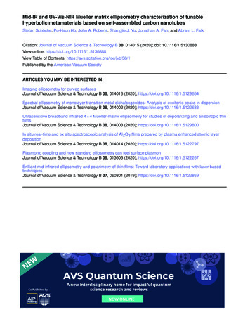
ARTICLEto parameterize each dielectric function tensor element.The regression analysis on the experimental data was then repeatedwith the new set of parameterized model dielectric functions. A setof Gaussian oscillators was found to best describe the line shape ofthe interband transitions and the π π w plasmon resonance,3622ε2 (E) ¼ An e ð(E En ) Brn Þ An e ð(EþEn ) Brn Þ :(3)The variable parameters for each oscillator are the center energy En ,the amplitude An , and the broadening Brn . The real part is calculatedusing the Kramers–Kronig integration. The well-known Drude modelis applied to match the free-carrier related absorption in the IR spectral range,31ε(E) ¼ h2:ε0 ρ(τE2 þ i hE)(4)The variable parameters for the Drude equation are the resistivity ρgiven in Ω cm and the average scattering time τ in femtoseconds.A constant offset ε1 and a pole function account for any offset anddispersion in the real part of the dielectric function tensoravs.scitation.org/journal/jvbcomponent due to absorption at higher energies outside the measured spectral range.31IV. RESULTS AND DISCUSSIONAn exemplary dataset of the Mueller matrix obtained for a203 nm film of ambient-doped crystallized CNTs is shown in Fig. 2for a photon energy of 0.73 eV. Experimental data for four anglesof incidence (solid lines) and the best-matching model-calculateddata (dotted lines) are shown for a full sample rotation. The dataare bound between 1 and þ1 due to normalization by the Muellermatrix element M11 (representative for total reflected unpolarizedintensity). Note the excellent agreement between the model and theexperiment for all rotation angles. A similar agreement was achievedover the entire measured spectral range from the mid-IR to the UV.Strong offdiagonal block elements indicate the highly anisotropicnature of these films. All Mueller matrix elements show a twofoldsymmetry indicated by the vertical markers in the second column inFig. 2, which proves the effective uniaxial optical properties of thefilm. Four rotation angles can be identified where all offdiagonalblock elements are identical to zero for all angles of incidenceFIG. 2. Normalized Mueller matrix data obtained on the UV-Vis-NIR ellipsometer for a 203 nm film of ambient-doped crystallized CNTs. Experimental data for four angles of incidence (solid lines) as well as the best-matching model data (dotted lines) are shown for the exemplary energy of 0.73 eV for a full 360 rotation of the sample. Vertical lines in thesecond column show the twofold symmetry of all Mueller matrix elements, and vertical lines in m13 and m23 mark the pseudoisotropic orientations in the off-diagonal blocks.J. Vac. Sci. Technol. B 38(1) Jan/Feb 2020; doi: 10.1116/1.5130888Published under license by AVS.38, 014015-4
ARTICLE(vertical lines in m13 and m23 in Fig. 2). These pseudoisotropicpoints prove that the optical axis is perfectly aligned in the surfaceplane as expected from the transmission electron microscopy images.From the spread of data vs the angle of incidence at f ¼ 0 , we caneasily identify that the optical axis was within the plane of incidenceat the beginning of the rotation scan even without a model analysis.A uniaxial dielectric function tensor model was applied tomatch experimental and model data. A Kramers–Kronig-consistentB-spline model with 0.1 eV node spacing was used for each tensorelement in order to obtain the best-matching model. The Eulerangle θ was assumed to be identical for all datasets, while theazimuthal angle f for the starting orientation of the full rotationscan in the NIR-Vis-UV spectral range and for each orientationof the mid-IR measurements was allowed to vary for each dataset.The thicknesses of the CNT layer and the surface roughness layerwere varied during the regression analysis but assumed to be identical for all datasets. The two independent tensor elements of thebest-matching model were then each parameterized with an appropriate number of Gaussian oscillators and a Drude absorption tailto account for free-carrier absorption in the IR spectral range.Eight Gaussian oscillators were necessary to match the parallelcomponent of the dielectric function tensor and seven Gaussianoscillators for the perpendicular component. The purpose of theparameterization is to extract values for the physical quantities ofaverage scattering time, resistivity, and the energies of the interbandtransitions and π π w plasmon.37 The line shape of the resultingdielectric function tensor components matches the B-spline extractedvalues nearly identically. Gaussian oscillators were chosen since theymatch the observed line shape well, and a Gaussian distribution oftransition energies would be expected for normally distributed radiiof CNT around the average radius.24Figure 3 shows the resulting dielectric function tensorelements for an ambient-doped sample of aligned but unorderedCNTs. The most prominent features in the dielectric functiontensor elements are due to electronic interband transitions andthe broad π π w plasmon absorption. In general, the absorptionFIG. 3. Real part (ε1 ) and imaginary part (ε2 ) of the dielectric function tensorelements parallel and perpendicular to the CNT axes for an ambient-doped40 nm film of aligned but not densely packed CNT. Known interband transitionsand the π π w plasmon absorption are marked by arrows. The hyperbolicranges are indicated by shading.J. Vac. Sci. Technol. B 38(1) Jan/Feb 2020; doi: 10.1116/1.5130888Published under license by AVS.avs.scitation.org/journal/jvbfeatures for polarization along the CNT axes are much strongerthan that for the perpendicular direction (note the logarithmicscale for ε2 ). Group theory predicts that for polarization along theCNT axis, optical transitions are only allowed between valence andconduction bands of an equal index, labeled Snn for semiconductingCNTs and Mnn for metallic CNTs, where n is the band index. Forpolarization perpendicular to the CNT axes, only transitions betweenthe valence band of index n and conduction bands of index n 1are expected. The strongest feature in the data located at 0.65 eV canbe assigned to the transition from the first valence to the first conduction band in semiconducting CNT, S11 . The energetic position isconsistent with theoretical predictions and experimental observationsfor CNTs of this diameter.14,18,24 Note that the absorption isexpected to be caused by excitons located slightly below the actualband-to-band transition energy but it is not possible to distinguishbetween exciton and band-to-band absorption using the ellipsometrytechnique. The next higher allowed transition S22 is found at 1.18 eVagain in agreement with earlier publications.14,18,24 Since the filmscontain a mix of semiconducting and metallic CNTs, we can alsoidentify the transition from the first valence to the conduction bandin metallic structures, M11 , in our data. This transition is located at1.67 eV. A broad absorption peak is observed in the range whereS33 and S44 are expected. The broad π π w plasmon absorption islocated at 4.32 eV for this polarization. A narrow distribution ofCNT diameters in our mix of CNTs can be concluded from the existence of relatively narrow and clearly defined peaks for the interbandtransitions.27 Despite the selection rules, for polarization perpendicular to the CNT axes, we can identify the same peaks as for theparallel component but with a much weaker amplitude. This is likelyrelated to a slight misalignment of the nanotubes in this unorderedfilm. In addition, we can identify two peaks that can be assigned tothe symmetry-allowed interband transitions S12 /S21 and S23 /S32 .Even these allowed transitions are much smaller in amplitude thanthe strong interband absorptions for polarization along the CNTaxes. Local field effects have to be taken into account to correctlydescribe the amplitude of absorption relative to the CNT axes.12,15A depolarization effect leads to strongly reduced electronic transitions for light polarized perpendicular to the CNT axes compared topolarization along the CNT axes resulting in very sharp and strongfeatures for absorption measurements with polarization parallel tothe nanotube axes and much smaller and very broad absorption forpolarization perpendicular to the nanotube axes.16 Intertube interactions can strongly modify the depolarization effect.15–17 The broadπ π w plasmon absorption for polarization perpendicular to theCNT axes is located at 4.79 eV, which is slightly higher than forpolarization along the CNT axes in agreement with theoreticalpredictions.16The hyperbolic ranges in the dielectric function tensor ofaligned but unordered CNTs are marked by shading in Fig. 3.A very wide range of hyperbolic dispersion between 3.81 and13.65 μm is found. This range is mainly caused by the largedifference in conductivity along the CNT axes and perpendicularto the CNT axes. The values for the resistivity obtained fromthe Drude model are ρk ¼ 3:0 10 4 Ω cm along the CNTaxes and ρ? ¼ 8:6 10 3 Ω cm perpendicular to the CNT axes.The relatively low resistivities in these ambient-doped films arecaused by the metallic CNT and ambient p-type doping in the38, 014015-5
ARTICLEsemiconducting CNT. For films of purely semiconducting CNTs,we would expect a shift of the hyperbolic range toward longerwavelengths. Average scattering times of τ k ¼ 13:8 fs andτ ? ¼ 5:2 fs are consistent with the picture of reduced conductivityperpendicular to the CNT axes. It has been demonstrated that theresistivity parameters obtained from contactless ellipsometrymeasurements agree within 6% with electrical point probe measurements in these films.26The obtained dielectric function tensor elements for a CNTsample of aligned and ordered (crystalline) CNTs are presented inFig. 4. Both ambient-doped and highly doped CNT films areshown. Compared to the unordered CNT film, the dielectric function tensor component parallel to the CNT axes is essentiallyunchanged for the ambient-doped film [Fig. 4(a)]. For the perpendicular direction, the contribution of transitions assigned to parallelpolarization is strongly reduced while the S12 /S21 and S23 /S32 transitions can still clearly be identified. This indicates the close to perfectalignment of the CNT in this sample. The width of the hyperbolicspectral range is slightly reduced due to a reduced resistivity ofρ? ¼ 4:1 10 3 Ω cm and an increased average scattering time ofτ ? ¼ 11:1 fs, indicating better conductivity perpendicular to theavs.scitation.org/journal/jvbCNT axes in the ordered film compared to the unordered case.Further, an additional small and very broad absorption featureappears in the mid-IR spectral range [indicated by the upwardspointing arrow in Fig. 4(a)]. The nature of this absorption feature isnot entirely clear and could be related to a plasmon absorptionrelated to the domain size of perfectly ordered CNTs (approximately25 nm in this sample), infrared absorption of covalently bound functional groups,27 or some other effects. Note that the amplitude ofthis absorption feature is relatively small a
limited spectral ranges using polarized transmission,20 polarized reflection,21 and polarized photoluminesence.22 Standard spectro-scopic ellipsometry measurements were performed on horizontally but randomly aligned CNTs with in-plane isotropic optical properties.18,