Transcription
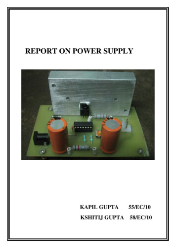
REPORT ON POWER SUPPLYKAPIL GUPTA55/EC/10KSHITIJ GUPTA58/EC/10
CONTENTS1. ABSTRACT2. INTRODUCTION2.1.Linear Power Supplies2.2. Switch Mode Power Supplies3.
ABSTRACTA power supply is a device that supplies electrical energy to one or more electric loads. Theterm is most commonly applied to devices that convert one form of electrical energy toanother, though it may also refer to devices that convert another form of energy (e.g.,mechanical, chemical, solar) to electrical energy.All electronic circuits from simple transistorand op amp circuits to elaborate digital and microprocessor systems require one or moresources of DC voltage . Simplest supply is a dc battery.It is not an ideal one as its terminalvoltage changes in accordance with load due to its internal resistance . Electroniccomponents require a DC supply that is well regulated, has low noise characteristics andprovides a fast response to load changes.A regulated power supply is one that controls the output voltage or current to a specificvalue; the controlled value is held nearly constant despite variations in either load currentor the voltage supplied by the power supply's energy source.Fortunately it is easy to construct a stable power supply using negative feedback .Suchoutput supplies are in universal use and can be constructed using voltage regulator IC s.Inthis report we will see how to use such special purpose voltage regulator IC s to constructstable power supplies .
INTRODUCTIONVirtually every piece of electronic equipment is powered from a low voltage DC supply. This sourcewill be either a battery, a combination of battery and DC/DC converter or a power supply convertingAC mains into one or more low voltage DC supplies, suitable for electronic components. AC powersupplies, and most DC/DC converters, also provide isolation from the input to the output for safety,noise reduction and transient protection.As electronic equipment has become smaller, the market has demanded that power converters dothe same. Since the introduction of switch mode techniques, this has been an evolutionary ratherthan a revolutionary process. Conversion efficiency has increased, materials and componentsallowing higher switching frequencies have become available and packaging techniques haveadvanced. At the same time, unit cost has fallen as volumes have increased. With the global marketfor electronics becoming a reality, power supply systems operate from wide input ranges to coverworldwide AC mains supply variations.There are a number of basic topologies used in power supplies , which are suited to various powerlevels, cost criteria and performance levels as discussed below:- Linear Power SuppliesLinear power supplies are typically only used in specific applications requiring extremely low noise,or in very low power applications where a simple transformer rectifier solution is adequate andprovides the lowest cost. Examples are audio applications (low noise) and low power consumerapplications such as alarm panels (low cost).
The 50/60Hz mains transformer reduces the voltage to a usable low level, the secondary AC voltageis rectified using a rectifier circuit and some form of circuit is employed to provide the necessaryregulation usually containing a voltage regulator IC’s.The benefits of this solution are low noise, reliability and low cost. On the downside, these units arelarge, heavy and inefficient with a limited input voltage range.In order to significantly reduce the size and increase efficiency, most applications utilize a SwitchMode Power Supply (SMPS). Switch Mode Power SuppliesThe use of switch mode topologies has reduced the size and improved the efficiency of powersupplies by increasing the frequency of operation, reducing the physical size of transformers,inductors and capacitors, and utilizing an ‘on or off’ switching element to increase efficiency.The compromises in adopting this technique are increased ripple and noise on the output DC supplyAs switching frequency increases, so do switching losses.The introduction of low voltage semiconductors and the consequent high output current demandshave driven the development of synchronous output rectifier schemes, where the output diodes arereplaced by power MOSFETs to reduce power dissipation in the secondary and achieve highefficiency solutions for these applications.
A general power supply unit has the following basic units. SOURCEEvery power supply must obtain the energy it supplies to its load, as well as any energy it consumeswhile performing that task, from an energy source. Depending on its design, a power supply mayobtain energy from:1.Electrical energy transmission systems. Common examples of this include power supplies thatconvert AC line voltage to DC voltage.2.Energy storage devices such as batteries and fuel cells.3.Electromechanical systems such as generators and alternators.Solar power. PROTECTIONInput protection is implemented in power supplies in order to ensure safety.The input fuse fittedwithin a power supply is not intended to be field-replaceable. It is rated such that only a catastrophicfailure of the power supply will cause it to fail. It cannot be damaged by overloading as the powersupply will have some other form of overload protection, usually electronic.The fuse will often besoldered into the PCB rather than being a replaceable cartridge type fuse.
RECTIFIERA rectifier is an electrical device that converts alternating current (AC), which periodically reversesdirection, to direct current (DC), which flows in only one direction.A bridge rectifier provides full-wave rectification from a two-wire AC input, resulting in lower costand weight as compared to a rectifier with a 3-wire input from a transformer with a center-tappedsecondary winding. FILTERINGThe R-C filter circuit as given in figure is used to reject input noise . By deliberate design R is keptmuch larger than XC1 at the ripple frequency. So the ripples are dropped across series resistor Rinstead of across the load resistor RL. Typically R is kept at least 10 times greater than XC2; thismeans that each section reduces the ripples by a factor of at least 10. REGULATIONIC 723 is a voltage regulator designed primarily for series regulator applications. it is a flexible, easyto use regulator with excellent performance. The circuit features a temperature-compensatedvoltage reference, differential amplifier, series pass transistor, and current-limiting protective circuit.By itself, it will supply output currents up to 150 mA; but external transistors can be added toprovide any desired load current as shown in the figure below
An external pass transistor Q1 is used. Q1 is added as a Darlington pair with the internal transistor .CIRCUIT OF POWER SUPPLY USING IC 723The external pass transistor must be mounted on a heat sink .723 does not incorporate internalshut-down circuitry to protect against excessive load current so provision is made for either linear orfoldback current limiting as discussed in output protection.
POSITIVE REGULATORFigure below shows how to make a positive voltage regulator with the 723.Voltage divider R1,R2compares a fraction of the output with the voltage reference , this circuit is identical with the opamp non inverting amplifier with Vref as the input to the non inverting terminal and a fraction ofoutput voltage to the inverting terminal . What it does is look at its input terminals and swing itsoutput terminal around so that the external feedback network brings the input differential to zeroThus we get a required regulated output .The input voltage must stay a few volts more positive than the output at all times, including theeffects of ripple on the unregulated supply .The "dropout voltage'' is 3 volts (minimum) for the 723NEGATIVE REGULATORFigure below shows how to make a negative voltage regulator with the 723.It’s working is similar tothe positive regulator. Voltage divider R1,R2 compares a fraction of the Vref with the output voltageThe input to the non inverting terminal is the output voltage and a fraction of Vref voltage goes tothe inverting terminal . What it does is look at its input terminals and swing its output terminalaround so that the external feedback network brings the input differential to zeroThus we get a required regulated output .
OUTPUT PROTECTIONOutput protection is implemented on power supplies and DC/DC converters in order to preventdamage to the power supply and the end equipment. Power supplies are protected against overloadand the end equipment against over-voltage and excessive fault current.OVERLOAD PROTECTIONIn the case of an overload or short circuit being applied to the output, circuits are employed to limitthe current or power that the unit will supply, protecting both the power supply and the load fromexcessive current. Cutting off drive to the pass transistors is used to limit output currents to nondestructive levels. OUTPUTUsing the above components a regulated supply with output voltage ranging from to the maximumallowable output voltage can be made. Obviously the choice of output is left for the requirement ofuser. The input voltage must stay a few volts more positive than the output at all times, including theeffects of ripple on the unregulated supply .Output current can be controlled by suitably choosingthe values of components
TESTING A POWER SUPPLYLINE REGULATIONLine regulation is a static performance measure of how well a power supply holds the output voltageConstant in the face of a changing input.Line regulation defines the change in output voltage or current resulting from a change in the inputVoltage over a specified range.% Line Regulation VOUT(Max)-VOUT(Min) / VOUT(Normal) x 100Where ,VOUT (Normal) is the output voltage at nominal line input voltageVOUT (Max) is the output voltage at maximum line input voltageVOUT (Min) is the output voltage at minimum line input voltageExample: A power supply’s output is nominally 5.02V but when the AC input is varied from itsminimum to maximum value the output varies from 5.015V to 5.03V.% Line Regulation ( 5.03 – 5.015 ) / 5.02 x 100 0.29 %LOAD REGULATION AND CROSS REGULATIONLoad regulation is a static performance measure, which defines the ability of a power supply toremain within specified output limits for a predetermined load change. Expressed as a percentage,the range is dependent upon the product design and is specified in the product data sheet.% Load Regulation VOUT(Load Max)-VOUT(Load Min) / VOUT(Normal) x 100Where,VOUT (Normal) is the nominal output voltageVOUT (Load Max) is the output voltage at maximum output currentVOUT (Load Min) is the output voltage at minimum output currentExample: A power supply manufacturer specifies that for a load change of 5% to 100% its powersupply output changes from 5.02V to 5.05V around a nominal voltage of 5.02V.% Load Regulation ( 5.05 – 5.02 ) / 5.02 x 100 0.6 %
For multiple output power supplies, another factor affecting the output voltage is cross regulation.This is an extension of the load regulation test and determines the ability of all the power supplyoutputs to remain within their specified voltage rating for a load current change on another output.It is calculated in the same manner as load regulation and is often specified as a percentage changein output voltage for a percentage change in another output load, e.g. V1 cross regulation 1% per10% change in V2.
CIRCUIT FOR A POWER SUPPLYUSING IC 723NOTE: Only one type of regulation can be used at a time.
SOURCESBOOKThe Art of Electronics, by Paul Horowitz and Winfield a.org/wiki/Power supplyhttp://en.wikipedia.org/wiki/Diode bridgehttp://en.wikipedia.org/wiki/Active load
In order to significantly reduce the size and increase efficiency, most applications utilize a Switch Mode Power Supply (SMPS). Switch Mode Power Supplies The use of switch mode topologies has reduced the size and improved the efficiency of power supplies by increasing the frequency