Transcription
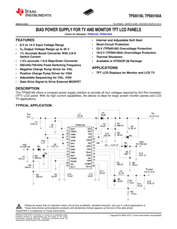
TPS65160, TPS65160Awww.ti.comSLVS566C – MARCH 2005 – REVISED MARCH 2013BIAS POWER SUPPLY FOR TV AND MONITOR TFT LCD PANELSCheck for Samples: TPS65160, TPS65160AFEATURES1 2 8-V to 14-V Input Voltage RangeVS Output Voltage Range up to 20 V1% Accurate Boost Converter With 2.8-ASwitch Current1.5% accurate 1.8-A Step-Down Converter500-kHz/750-kHz Fixed Switching FrequencyNegative Charge Pump Driver for VGLPositive Charge Pump Driver for VGHAdjustable Sequencing for VGL, VGHGate Drive Signal to Drive External MOSFET Internal and Adjustable Soft StartShort-Circuit Protection23-V (TPS65160) Overvoltage Protection19.5-V (TPS65160A) Overvoltage ProtectionThermal ShutdownAvailable in HTSSOP-28 PackageAPPLICATIONS TFT LCD Displays for Monitor and LCD TVDESCRIPTIONThe TPS65160 offers a compact power supply solution to provide all four voltages required by thin-film transistor(TFT) LCD panel. With its high current capabilities, the device is ideal for large screen monitor panels and LCDTV applications.TYPICAL APPLICATIONC12*22 FVGL 5 V/50 mAC31 FC161 FD2TPS65160812202122C60.47 F1691113246D3C7470 FD1SL22L110 HVIN12 VR3620 k 72825R4150 k C8220 nFC922 C1010 nF4SW5SW1FBOS 2 26C1110 nFVS15 V/1.5 AR1680 k C422 pFC15470 nFC23* 22 FR256 k D4VGH23 V/50 mAD5C50.47 FR51 M Cb100 nFC1722 nFC130.47 FR656 k VLOGICL215 HD6SL223.3 V/1.5 AR72 k C1410 nFC122*22 FR81.2 k 12Please be aware that an important notice concerning availability, standard warranty, and use in critical applications ofTexas Instruments semiconductor products and disclaimers thereto appears at the end of this data sheet.PowerPAD is a trademark of Texas Instruments.PRODUCTION DATA information is current as of publication date.Products conform to specifications per the terms of the TexasInstruments standard warranty. Production processing does notnecessarily include testing of all parameters.Copyright 2005–2013, Texas Instruments Incorporated
TPS65160, TPS65160ASLVS566C – MARCH 2005 – REVISED MARCH 2013www.ti.comThis integrated circuit can be damaged by ESD. Texas Instruments recommends that all integrated circuits be handled withappropriate precautions. Failure to observe proper handling and installation procedures can cause damage.ESD damage can range from subtle performance degradation to complete device failure. Precision integrated circuits may be moresusceptible to damage because very small parametric changes could cause the device not to meet its published specifications.DESCRIPTION (CONTINUED)The device can be powered directly from a 12-V input voltage generating the bias voltages VGH and VGL, aswell as the source voltage VS and logic voltage for the LCD panels. The device consists of a boost converter toprovide the source voltage VS and a step-down converter to provide the logic voltage for the system. A positiveand a negative charge-pump driver provide adjustable regulated output voltages VGL and VGH to bias the TFT.Both boost and step-down converters, as well as the charge-pump driver, operate with a fixed switchingfrequency of 500 kHz or 750 kHz, selectable by the FREQ pin. The TPS65160 includes adjustable power-onsequencing. The device includes safety features like overvoltage protection of the boost converter and shortcircuit protection of the buck converter, as well as thermal shutdown. Additionally, the device incorporates a gatedrive signal to control an isolation MOSFET switch in series with VS or VGH. See the application circuits at theend of this data sheet.ORDERING INFORMATIONTA–40 C to 85 C(1)(1)UVLO(typ)Overvoltage protectionVs (typ)ORDERINGPACKAGE (2)PACKAGEMARKING6V23 VTPS65160PWPHTSSOP28 (PWP)TPS651608V19.5 VTPS65160APWPHTSSOP28 (PWP)TPS65160AFor the most current package and ordering information, see the Package Option Addendum at the end of this document, or see the TIwebsite at www.ti.com.The PWP package is available taped and reeled. Add R-suffix to the device type (TPS65160PWPR) to order the device taped andreeled. The TPS65160PWPR package has quantities of 2000 devices per reel. Without suffix, the TPS65160PWP is shipped in tubeswith 50 devices per tube.(2)ABSOLUTE MAXIMUM RATINGSover operating free-air temperature range (unless otherwise noted) (1)UNITVoltages on pin VIN, SUP (2)–0.3 V to 16.5 VVoltages on pin EN1, EN2, FREQ (2)Voltage on pin SW–0.3 V to 15 V(2)25 VVoltage on pin SWB (2)20 VVoltages on pin OS, GD (2)25 VContinuous power dissipationSee Dissipation Rating TableTAOperating junction temperature–40 C to 150 CTstgStorage temperature range–65 C to 150 CTemperature (soldering, 10 s)(1)(2)260 CStresses beyond those listed under absolute maximum ratings may cause permanent damage to the device. These are stress ratingsonly, and functional operation of the device at these or any other conditions beyond those indicated under recommended operatingconditions is not implied. Exposure to absolute-maximum-rated conditions for extended periods may affect device reliability.All voltage values are with respect to network ground terminal.DISSIPATION RATINGS(1)2PACKAGERTHJATA 25 CPOWER RATINGTA 70 CPOWER RATINGTA 85 CPOWER RATING28-Pin HTSSOP28 C/W (PowerPAD (1) soldered)3.57 W1.96 W1.42 WSee Texas Instruments application report SLMA002 regarding thermal characteristics of the PowerPAD package.Submit Documentation FeedbackCopyright 2005–2013, Texas Instruments IncorporatedProduct Folder Links: TPS65160 TPS65160A
TPS65160, TPS65160Awww.ti.comSLVS566C – MARCH 2005 – REVISED MARCH 2013RECOMMENDED OPERATING CONDITIONSover operating free-air temperature range (unless otherwise noted)MINVSOutput voltage range of the main boost converterNOMMAXTPS65160TPS65160AVSUPMaximum operating voltage at the charge-pump driver supply pin SUPInput capacitor AVINLVLOGICCOVVV2x22µF1µFInductor boost converter (1)10Inductor buck converter (1)15Output voltage range of the step-down converter VLOGIC2017.515Input capacitor at VINBCINUNITµH1.85.0Output capacitor boost converter3x22Output capacitor buck converter2x22VµFTAOperating ambient temperature–4085 CTJOperating junction temperature–40125 C(1)See application section for further information.ELECTRICAL CHARACTERISTICSVIN 12 V, SUP VIN, EN1 EN2 VIN, VS 15 V, VLOGIC 3.3 V, TA –40 C to 85 C, typical values are at TA 25 C(unless otherwise noted)PARAMETERTEST CONDITIONSMINTYPMAXUNITSUPPLY CURRENTVINInput voltage rangeTPS65160TPS65160AISUP14V14VQuiescent current into AVINVGH 2 VS,Boost converter notswitching0.2Quiescent current into VINBVGH 2 VS,Buck converter notswitching0.20.5Shutdown current into AVINEN1 EN2 GND0.12Shutdown current into VINBEN1 EN2 GND0.12Shutdown current into SUPEN1 EN2 GND0.14µAQuiescent current into SUPVGH 2 oltage lockout thresholdVREFReference voltageTPS65160VIN fallingTPS65160AVIN fallingmA1.203Thermal shutdown2Temperature risingThermal shutdown hysteresisµAV155 C5 CLOGIC SIGNALS EN1, EN2, FREQVIHHigh-level input voltage EN1, EN2VILLow-level input voltage EN1, EN2VIHHigh-level input voltage FREQVILLow-level input voltage .2µA6912µAEN1 EN2 FREQ GND or VINInput leakage currentVCONTROL AND SOFT START DLY1, DLY2, SSIDLY1Delay1 charge currentIDLY2Delay2 charge currentISSSS charge currentVTHRESHOLD 1.213 VCopyright 2005–2013, Texas Instruments IncorporatedProduct Folder Links: TPS65160 TPS65160ASubmit Documentation Feedback3
TPS65160, TPS65160ASLVS566C – MARCH 2005 – REVISED MARCH 2013www.ti.comELECTRICAL CHARACTERISTICS (continued)VIN 12 V, SUP VIN, EN1 EN2 VIN, VS 15 V, VLOGIC 3.3 V, TA –40 C to 85 C, typical values are at TA 25 C(unless otherwise noted)PARAMETERTEST CONDITIONSMINTYPMAXFREQ high600750900FREQ low400500600UNITINTERNAL OSCILLATORfOSCOscillator frequencykHzBOOST CONVERTER (VS)VSOutput voltage rangeVFBFeedback regulation voltageIFBFeedback input bias .156V10100nAN-MOSFET on-resistance (Q1)ISW 500 mA100185mΩP-MOSFET on-resistance (Q2)ISW 200 mA1016Ω1AIMAXMaximum P-MOSFET peak switch currentILIMN-MOSFET switch current limit (Q1)IleakSwitch leakage currentVovpOvervoltage protection2.8VSW 15 V3.54.2A110µATPS65160VOUT rising222324.5VTPS65160AVOUT rising1819.520.5VLine regulation10.6 V Vin 11.6 Vat 1 mALoad regulation0.0008%/V0.03%/AGATE DRIVE (GD)VGDGate drive threshold (1)VFB risingVOLGD output low voltageI(sink) 500 µAGD output leakage currentVGD 20 WN CONVERTER (VLOGIC)VLOGICOutput voltage rangeVFBBFeedback regulation voltage1.8IFBBFeedback input bias currentrDS(ON)N-MOSFET on-resistance (Q1)ILIMN-MOSFET switch current limit (Q1)IleakSwitch leakage currentVSW 0 VLine regulation10.6 V VIN 11.6 Vat 1 mA1.195ISW 500 mA2Load %/V0.037%/AThe GD signal is latched low when the main boost converter output VS is within regulation. The GD signal is reset when the inputvoltage or enable of the boost converter is cycled low.Submit Documentation FeedbackCopyright 2005–2013, Texas Instruments IncorporatedProduct Folder Links: TPS65160 TPS65160A
TPS65160, TPS65160Awww.ti.comSLVS566C – MARCH 2005 – REVISED MARCH 2013ELECTRICAL CHARACTERISTICS (continued)VIN 12 V, SUP VIN, EN1 EN2 VIN, VS 15 V, VLOGIC 3.3 V, TA –40 C to 85 C, typical values are at TA 25 C(unless otherwise noted)PARAMETERTEST IVE CHARGE-PUMP VGLVGLOutput voltage rangeVFBNFeedback regulation voltageIFBNFeedback input bias currentrDS(ON)Q4 P-Channel switch rDS(ON)VDropN(2)Current sink voltage dropΩIOUT 20 mA4.4IDRN 50 mA,VFBN VFBNnominal –5%130190IDRN 100 mA,VFBN VFBNnominal –5%2704201.2131.238V10100nAmVPOSITIVE CHARGE-PUMP OUTPUT VGHVFBPFeedback regulation voltageIFBPFeedback input bias currentrDS(ON)Q3 N-Channel switch rDS(ON)VDropPCurrent source voltage drop(Vsup – VDRP) (3)ΩIOUT 20 mA1.1IDRP 50 mA,VFBP VFBPnominal –5%400680IDRP 100 mA,VFBP VFBPnominal –5%8501600mVThe maximum charge-pump output current is typically half the drive current of the internal current source or current sink.The maximum charge-pump output current is typically half the drive current of the internal current source or current 1118SWBFREQ1217BOOTFBN1316EN1FBP1415FBBThermal PAD (see Note)(2)(3)1.187NOTE: The thermally enhanced PowerPAD is connected to PGND.Copyright 2005–2013, Texas Instruments IncorporatedProduct Folder Links: TPS65160 TPS65160ASubmit Documentation Feedback5
TPS65160, TPS65160ASLVS566C – MARCH 2005 – REVISED MARCH 2013www.ti.comTERMINAL FUNCTIONSTERMINALNAMENO.I/ODESCRIPTIONSUP8IThis is the supply pin of the positive and negative charge-pump driver and can be connected to the input or outputof the TPS65160 main boost converter. Because the SUP pin is rated to a maximum voltage of 15 V, it needs tobe connected to the input of the TPS65160 for an output voltage greater than 15 V.FREQ12IFrequency adjust pin. This pin allows setting the switching frequency with a logic level to 500 kHz low and750 kHz high.AVIN22IAnalog input voltage of the device. This is the input for the analog circuits of the device and should be bypassedwith a 1-μF ceramic capacitor for good filtering.VINB20, 21IPower input voltage pin for the buck converter.EN116IThis is the enable pin of the buck converter and negative charge pump. When this pin is pulled high, the buckconverter starts up, and after a delay time set by DLY1, the negative charge pump comes up. This pin must beterminated and not be left floating. A logic high enables the device and a logic low shuts down the device.EN29IThe boost converter starts only with EN1 high, after the step-down converter is enabled. EN2 is the enable pinof the boost converter and positive charge pump. When this pin is pulled high, the boost converter and positivecharge pump starts up after the buck converter is within regulation and a delay time set by DLY2 has passed by.This pin must be terminated and not be left floating. A logic high enables the device and a logic low shuts downthe device.DRN11ODrive pin of the negative charge pump.FBN13IFeedback pin of negative charge pump.REF24OInternal reference output typically 1.213 VPGND6, 7SS28OThis pin allows setting the soft-start time for the main boost converter VS. Typically a 22-nF capacitor needs to beconnected to this pin to set the soft-start time.DLY125OConnecting a capacitor from this pin to GND allows the setting of the delay time between VLOGIC (step-downconverter output high) to VGL during start-up.DLY226OConnecting a capacitor from this pin to GND allows the setting of the delay time between VLOGIC (step-downconverter output high) to VS Boost converter and positive charge-pump VGH during start-up.COMP2FBB15IFeedback pin of the buck converterSWB18OSwitch pin of the buck converterNC19BOOT17FBPDRPGD27This is the gate drive pin which can be used to control an external MOSFET switch to provide input to outputisolation of VS or VGH. See the circuit diagrams at the end of this data sheet. GD is an open-drain output and islatched low as soon as the boost converter is within 8% of its nominal regulated output voltage. GD goes highimpedance when the EN2 input voltage is cycled low.GND23Analog groundOS3IOutput sense pin. The OS pin is connected to the internal rectifier switch and overvoltage protection comparator.This pin needs to be connected to the output of the boost converter and cannot be connected to any other voltagerail. Connect a 470-nF capacitor from OS pin to GND to avoid noise coupling into this pin. The PCB trace of theOS pin needs to be wide because it conducts high current.FB1IFeedback of the main boost converter generating Vsource (VS).SW4, 5ISwitch pin of the boost converter generating Vsource (VS).PowerPAD6Power groundThis is the compensation pin for the main boost converter. A small capacitor and, if required, a resistor isconnected to this pin.Not connectedIN-channel MOSFET gate drive voltage for the buck converter. Connect a capacitor from the switch node SWB tothis pin.14IFeedback pin of positive charge pump.10ODrive pin of the positive charge pump.The PowerPAD needs to be connected and soldered to power ground (PGND).Submit Documentation FeedbackCopyright 2005–2013, Texas Instruments IncorporatedProduct Folder Links: TPS65160 TPS65160A
TPS65160, TPS65160Awww.ti.comSLVS566C – MARCH 2005 – REVISED MARCH 2013TYPICAL CHARACTERISTICSTable 1. TABLE OF GRAPHSFIGUREMAIN BOOST CONVERTER (Vs)ηEfficiency main boost converter Vsvs Load current VS 15 V,VIN 12 V1rDS(ON)N-channel main switch Q1vs Input voltage and temperature2Soft-start boost converterCSS 22 nF3PWM operation at full-load current4PWM operation at light-load current5Load transient response6STEP-DOWN CONVERTER (Vlogic)ηEfficiency main boost converter VSINrDS(ON)N-channel main switch Q1vs Load current VLOGIC 3.3 V,V 12 V78PWM operation - continuous mode9PWM operation - discontinuous mode10Soft start11Load transient response12SYSTEM PERFORMANCEfoscOscillation frequencyvs Input voltage and temperature13Power-up sequencingEN2 connected to VIN14Power-up sequencingEN2 enabled seperately15BOOST CONVERTERrDS(ON) - N-CHANNEL SWITCHvsTEMPERATUREBOOST CONVERTER EFFICIENCYvsOUTPUT CURRENT1000.16900.14rDS(on) N-Channel Switch Ω80Efficiency %7060504030VI 12 V,VO 15 V,L 10 H200.511.50.120.10.080.060.040.021000VI 8 V,VI 12 V,VI 14 V20 40 20IO Output Current AFigure 1.020406080100 120 140TA Temperature 5CFigure 2.Copyright 2005–2013, Texas Instruments IncorporatedProduct Folder Links: TPS65160 TPS65160ASubmit Documentation Feedback7
TPS65160, TPS65160ASLVS566C – MARCH 2005 – REVISED MARCH 2013www.ti.comSOFT-STARTBOOST CONVERTERPWM OPERATION BOOST CONVERTERCONTINUOUS MODEVI 12 V,VO 15 V/1.5 AVI 12 V,VO 15 V/ 1.2 A,C(SS) 22 nFVSW10 V/divVO50 mV/divVS5 V/divI(Inductor)1 A/divII1 A/div1 ms/div2 ms/divFigure 3.Figure 4.PWM OPERATION BOOST CONVERTERCONTINUOUS MODE: LIGHT LOADLOAD TRANSIENT RESPONSE BOOST CONVERTERVI 12 V, VS 15 V,CO 3*22 mF,C(comp) 22 nF,L 6.8 mH,FREQ HighVI 3.3 V,VO 10 V/10 mAVSW10 V/divVS200 mV/divVO50 mV/divI(Inductor)1 A/divIL500 mA/div100 ms/div1 ms/divFigure 5.8Submit Documentation FeedbackFigure 6.Copyright 2005–2013, Texas Instruments IncorporatedProduct Folder Links: TPS65160 TPS65160A
TPS65160, TPS65160Awww.ti.comSLVS566C – MARCH 2005 – REVISED MARCH 2013STEP-DOWN CONVERTERrDS(ON) - N-CHANNEL SWITCHvsTEMPERATUREEFFICIENCY STEP-DOWN CONVERTERvsLOAD CURRENT900.25VI 8 V,VI 12 V,VI 14 VrDS(on) N-Channel Switch Ω8070Efficiency %6050403020VI 12 V,VO 3.3 V,L 15 mH10000.511.5IO Output Current A20.20.150.10.050 40 20020406080100 120 140TA Temperature 5CFigure 7.Figure 8.STEP-DOWN CONVERTERPWM OPERATIONCONTINUOUS MODESTEP-DOWN CONVERTERPWM OPERATIONDISCONTINUOUS MODEVI 12 V,VO 3.3 V/45 mAVSW5 V/divVSW5 V/divVO20 mV/divVO20 mV/divVI 12 V,VO 3.3 V/1.5 AI(Inductor)1 A/divI(Inductor)100 mA/div500 ns/div500 ns/divFigure 9.Figure 10.Copyright 2005–2013, Texas Instruments IncorporatedProduct Folder Links: TPS65160 TPS65160ASubmit Documentation Feedback9
TPS65160, TPS65160ASLVS566C – MARCH 2005 – REVISED MARCH 2013www.ti.comSOFT-STARTSTEP-DOWN CONVERTERLOAD TRANSIENT RESPONSESTEP-DOWN CONVERTERVI 12 V,VO 3.3 V/1.2 AVO1100 mV/divVI 12 V, V(logic) 3.3 V,CO 2*22 mF, FREQ HighVO1 V/divIO270 mA to 1.3 AI(Inductor)1 A/div50 ms/div200 ms/divFigure 11.Figure 12.SWITCHING FREQUENCYvsTEMPERATUREPOWER-UP SEQUENCINGEN2 CONNECTED TO VIN740Switching Frequency kHz735VI 8 V,VI 12 V,VI 14 V730V Logic2 V/div725VGL5 V/div720715710VS5 V/div705VGH10 V/div700695 50050100TA Temperature 5C1502 ms/divFigure 13.10Submit Documentation FeedbackFigure 14.Copyright 2005–2013, Texas Instruments IncorporatedProduct Folder Links: TPS65160 TPS65160A
TPS65160, TPS65160Awww.ti.comSLVS566C – MARCH 2005 – REVISED MARCH 2013POWER-UP SEQUENCINGEN2 ENABLED SEPARATELYV Logic2 V/divVS5 V/divVGH5 V/divEN22 V/div1 ms/divFigure 15.Copyright 2005–2013, Texas Instruments IncorporatedProduct Folder Links: TPS65160 TPS65160ASubmit Documentation Feedback11
TPS65160, TPS65160ASLVS566C – MARCH 2005 – REVISED MARCH 2013www.ti.comBLOCK DIAGRAMAVINSWSWQ2ClockDLY1DSSBiasVref 1.213 VThermalShutdownSequencingGNDFREQ500 kHz/750 kHzOscillatorCurrent LimitandSoft ontrol LogicSSAVINVrefDSCOMPPGNDQ1PGNDGM AmplifierComparatorSawtoothGeneratorFBVFB1.154 VPositiveCharge PumpOSSUPSUPI DRVPGM AmplifierLow GainVFB1.154CurrentControlSoft StartVref1.2 13 VDRVPQ3VINBVINBNegativeCharge PumpFBPStep-DownConverterCurrentControlSoft StartDRVNNRegulator8VBOOTI DRVNDQ3SSUPSWBControl LogicFBNNCCurrent LimitVref1.2 13 VRefIDLYDLY1DLY1VrefCompensationandSoft StartClock/2IDLY0.9 VVrefLogicSawtoothGeneratorClock0.6 VVref1.2 13 VClock Select During Short Circuitand Soft StartEN1Submit Documentation BBError AmplifierVrefVREFEN2Copyright 2005–2013, Texas Instruments IncorporatedProduct Folder Links: TPS65160 TPS65160A
TPS65160, TPS65160Awww.ti.comSLVS566C – MARCH 2005 – REVISED MARCH 2013DETAILED DESCRIPTIONBoost ConverterThe main boost converter operates in pulse-width modulation (PWM) and at a fixed switching frequency of500 kHz or 750 kHz set by the FREQ pin. The converter uses an unique fast response, voltage-mode controllerscheme with input voltage feedforward. This achieves excellent line and load regulation (0.03%-A load regulationtypical) and allows the use of small external components. To add higher flexibility to the selection of externalcomponent values, the device uses external loop compensation. Although the boost converter looks like anonsynchronous boost converter topology operating in discontinuous conduction mode at light load, theTPS65160 maintains continuous conduction even at light-load currents. This is achieved with a novel architectureusing an external Schottky diode with an integrated MOSFET in parallel connected between SW and OS. Seethe Functional Block Diagram. The intention of this MOSFET is to allow the current to go negative that occurs atlight-load conditions. For this purpose, a small integrated P-Channel MOSFET with typically 10-Ω rDS(on) issufficient. When the inductor current is positive, the external Schottky diode with the lower forward voltageconducts the current. This causes the converter to operate with a fixed frequency in continuous conduction modeover the entire load current range. This avoids the ringing on the switch pin as seen with standardnonsynchronous boost converter and allows a simpler compensation for the boost converter.Soft Start (Boost Converter)The main boost converter has an adjustable soft start to prevent high inrush current during start-up. The soft-starttime is set by the external capacitor connected to the SS pin. The capacitor connected to the SS pin is chargedwith a constant current that increases the voltage on the SS pin. The internal current limit is proportional to thevoltage on the soft-start pin. When the threshold voltage of the internal soft-start comparator is reached, the fullcurrent limit is released. The larger the soft-start capacitor value, the longer the soft-start time.Overvoltage Protection of the Boost ConverterThe main boost converter has an overvoltage protection to protect the main switch Q2 at pin (SW) in case thefeedback (FB) pin is floating or shorted to GND. In such an event, the output voltage rises and is monitored withthe overvoltage protection comparator over the OS pin. See the functional block diagram. As soon as thecomparator trips at typically 23 V, TPS65160, (19 V, TPS65160A), the boost converter turns the N-ChannelMOSFET switch off. The output voltage falls below the overvoltage threshold and the converter continues tooperate.Frequency Select Pin (FREQ)The frequency select pin (FREQ) allows setting the switching frequency of the entire device to 500 kHz (FREQ low) or 750 kHz (FREQ high). A lower switching frequency gives a higher efficiency with a slightly reduced loadtransient regulation.Thermal ShutdownA thermal shutdown is implemented to prevent damage caused by excessive heat and power dissipation.Typically, the thermal shutdown threshold is 155 C.Step-Down ConverterThe nonsynchronous step-down converter operates at a fixed switching frequency using a fast response voltagemode topology with input voltage feedforward. This topology allows simple internal compensation, and it isdesigned to operate with ceramic output capacitors. The converter drives an internal 2.6-A N-channel MOSFETswitch. The MOSFET driver is referenced to the switch pin SWB. The N-channel MOSFET requires a gate drivevoltage higher than the switch pin to turn the N-Channel MOSFET on. This is accomplished by a bootstrap gatedrive circuit running of the step-down converter switch pin. When the switch pin SWB is at ground, the bootstrapcapacitor is charged to 8 V. This way, the N-channel gate drive voltage is typically around 8 V.Copyright 2005–2013, Texas Instruments IncorporatedProduct Folder Links: TPS65160 TPS65160ASubmit Documentation Feedback13
TPS65160, TPS65160ASLVS566C – MARCH 2005 – REVISED MARCH 2013www.ti.comSoft Start (Step-Down Converter)To avoid high inrush current during start-up, an internal soft start is implemented in the TPS65160. When thestep-down converter is enabled over EN1, its reference voltage slowly rises from zero to its power-goodthreshold of typically 90% of Vref. When the reference voltage reaches this power-good threshold, the erroramplifier is released to its normal operation at its normal duty cycle. To further limit the inrush current during softstart, the converter frequency is set to 1/4th of the switching frequency fs and then 1/2 of fs determined by thecomparator that monitors the feedback voltage. See the internal block diagram. Soft start is typically completedwithin 1 ms.Short-Circuit Protection (Step-Down Converter)To limit the short-circuit current, the device has a cycle-by-cycle current limit. To avoid the short-circuit currentrising above the internal current limit when the output is shorted to GND, the switching frequency is reduced aswell. This is implemented by two comparators monitoring the feedback voltage. The step-down converterswitching frequency is reduced to 1/2 of fs when the feedback is below 0.9 V and to 1/4th of the switchingfrequency when the feedback voltage is below 0.6 V.Positive Charge PumpThe positive charge pump provides a regulated output voltage set by the external resistor divider. Figure 16shows an extract of the positive charge-pump driver circuit. The maximum voltage which can be applied to thecharge-pump driver supply pin, SUP, is 15 V. For applications where the boost converter voltage Vs is higherthan 15 V, the SUP pin needs to be connected to the input. The operation of the charge-pump driver can beunderstood best with Figure 16. During the first cycle, Q3 is turned on and the flying capacitor Cfly charges to thesource voltage, Vs. During the next clock cycle, Q3 is turned off and the current source charges the drive pin,DRP, up to the supply voltage, VSUP. Because the flying capacitor voltage sits on top of the drive pin voltage,the maximum output voltage is Vsup Vs.SUP Vin for Vs 15 VSUP Vs for Vs 15 VVsI DRVPDRPCurrentControlSoft StartCflyVGVGH23 V/50 mAQ3R5C130.47 mFFBPR6Figure 16. Extract of the Positive Charge-Pump DriverIf higher output voltages are required, another charge-pump stage can be added to the output.Setting the output voltage:Ǔǒ1 ) R5R6V out 1.213R5 R614ǒVoutVFBǓ*1 R6Submit Documentation FeedbackǒV out1.213Ǔ*1Copyright 2005–2013, Texas Instruments IncorporatedProduct Folder Links: TPS65160 TPS65160A
TPS65160, TPS65160Awww.ti.comSLVS566C – MARCH 2005 – REVISED MARCH 2013Negative Charge PumpThe negative charge pump provides a regulated output voltage set by the external resistor divider. The negativecharge pump operates similar to the positive charge pump with the difference that the voltage on the supply pin,SUP, is inverted. The maximum negative output voltage is VGL (–VSUP) Vdrop. Vdrop is the voltage dropacross the external diodes and internal charge-pump MOSFETs. In case VGL needs to be lower than –VS, anadditional charge-pump stage needs to be added.Setting the output voltage:R3 * 1.213 VV out *VREF R4 Vout Vout R3 R4 R41.213VREFR3R4The lower feedback resistor value, R4, should be in a range between 40 kΩ to 120 kΩ or the overall feedbackresistance should be within 500 kΩ to 1 MΩ. Smaller values load the reference too heavily, and larger valuesmay cause stability problems. The negative charge pump requires two external Schottky diodes. The peakcurrent rating of the Schottky diode has to be twice the load current of the output. For a 20-mA output current,the dual-Schottky diode BAT54 is a good choice.Power-On Sequencing (EN1, EN2, DLY1, DLY2)The TPS65160 has an adjustable power-on sequencing set by the capacitors connected to DLY1 and DLY2 andcontrolled by EN1 and EN2. Pulling EN1 high enables the step-down converter and then the negative chargepump driver. DLY1 sets the delay time between the step-down converter and negative charge-pump driver. EN2enables the boost converter and positive charge-pump driver at the same time. DLY2 sets the delay timebetween the step-down converter Vlogic and the boost converter Vs. This is especially useful to adjust the delaywhen EN2 is always connected to Vin. If EN2 goes high after the step-down converter is already enabled, thenthe delay DLY2 starts when EN2 goes high. See Figure 17 and Figure 18.EN2EN1DLY2VGHV s, VGHVsVinVinVo4Fall Time Depends on LoadCurrent and Feedback ResistorVGLDLY1GDFigure 17. Power-On Sequencing With EN2 Always High (EN2 Vin)Copyright 2005–2013, Texas Instruments IncorporatedProduct Folder Links: TPS65160 TPS65160ASubmit Documentation Feedback15
TPS65160, TPS65160ASLVS566C – MARCH 2005 – REVISED MARCH 2013www.ti.comEN2EN1DLY2VGHVsVGH ,VsVinVinFall Time Depends on LoadCurrent and Feedback ResistorVo4DLY1VGLGDFigure 18. Power-On Sequencing Using EN1 and EN2Setting the Delay Times DLY1, DLY2Connecting an external capacitor to the DLY1 and DLY2 pins sets the delay time. If no delay time is required,these pins can be left open. To set the delay time, the external capacitor connected to DLY1 and DLY2 ischarged with a constant current source of typically 4.8 µA. The delay time is terminated when the capacitorvoltage has reached the internal reference voltage of Vref 1.213 V. The external delay capacitor is calculated:4.8 mA td4.8 mA tdC with td Desired delay timedlyVref1.213 VExample for setting a delay time of 2.3 mS:4.8 mA 2.3 msC 9.4 nF å Cdly 10 nFdly1.213 VGate Drive Pin (GD)This is an open-drain output that goes low when the boost converter, Vs, is within regulation. The gate drive pinGD remains low until the input voltage or enable EN2 is cycled to ground.Undervoltage LockoutTo avoid misoperation of the device at low input voltages, an undervoltage lockout is included which shuts downthe device at voltages lower than 6 V.Input Capacitor SelectionFor good input voltage filtering, low ESR ceramic capacitors are recommended. The TPS65160 has an analoginput, AVIN, and two input pins for the buck converter VINB. A 1-µF input capacitor should be connected directlyfrom the AVIN to GND. Two 22-µF ceramic capacitors are connected in parallel from the buck converter inputVINB to GND. For better input voltage filtering, the input capacitor values can be increased. See Table 2 and theApplication Information section for input capa
The TPS65160 offers a compact power supply solution to provide all four voltages required by thin-filmtransistor (TFT) LCD panel. With its high current capabilities, the device is ideal for large screen monitor panels and LC