Transcription
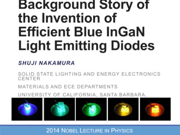
Background Story ofthe Invention ofEfficient Blue InGaNLight Emitting DiodesSHUJI NAKAMURAS O L I D S TAT E L I G H T I N G A N D E N E R G Y E L E C T R O N I C SCENTERM AT E R I A L S A N D E C E D E PA RT M E N T SU N I V E R S I T Y O F C A L I F O R N I A , S A N TA B A R B A R A ,U.S.A.2014 NOBEL LECTURE IN PHYSICS
Outline1) Introduction: What is an LED?2) Material of Choice: ZnSe vs. GaN3) The Beginning: GaN on Sapphire4) Enabling the LED: InGaN5) Historical Perspective
The LEDENERGY EFFICIENT WHITE LIGHT
What is an LED?A Light Emitting Diode (LED) produces light of a single color bycombining holes and electrons in a semiconductor.Source of Holes(p-type Layer)ExternalSource ofElectrons(Battery)Light OutCombining ofHoles and Electrons(Active / Emitting Layer)Substrate(Foundation)Source of Electrons(n-type Layer)
What is an LED?A Light Emitting Diode (LED) produces light of a single color bycombining holes and electrons in a semiconductor.Actual Blue LEDSize: 0.4 mm x 0.4 mmPackaged Blue LED
White LED: Combining ColorsWhite Light: Blue Other colors (red, yellow, green)Other Colors: Convert Blue LED Light to Yellow using Phosphor.Blue LEDPhosphorConvert:Blue YellowWhite Light Blue YellowWhite LEDS. Pimputkar et al., Nature Photonics 3 (2009) 180—182
Applications for InGaN-Based LEDsSolid State LightingDecorative LightingAutomobile LightingDisplaysAgricultureIndoor Lighting
Energy Savings Impact 40 % Electricity Savings (261 TWh) in USA in 2030 due to LEDsEliminates the need for 30 1000 MW Power Plants by 2030Avoids Generating 185 million tons of CO2Sources: www.nobelprize.org, US Department of Energy
1980s:ZnSe vs. GaNII-VIVS .III-N IN THE LATE ‘80S
Candidates for Blue LEDs: ZnSe vs.GaNSemiconductors that possess the required propertiesto efficiently generate blue light: ZnSe and GaNBUT How does one create ZnSe / GaN?Single crystal growth of material on top of different, available single crystal:Dislocation /DefectZnSeGaNGaAsAl2O3(Sapphire)0 % Lattice MismatchFew Dislocations (Defects)16 % Lattice MismatchSignificant Dislocations (Defects)
GaN on Sapphire: Heavily DefectedToo manyDislocations/DefectsGaN1 µmCross section Transmission Electron Microscope (TEM) of GaN on Sapphire, F. Wu et al., UCSBSapphire(Al2O3)
1989: ZnSe vs. GaN for Blue LEDZnSe on GaAs Substrate High Crystal Quality: Dislocation density 1x103 cm-2 Very Active Research: 99 % of researchersGaN on Sapphire Substrate Poor Crystal Quality: Dislocation density 1x109 cm-2 Little Research: 1 % of researchersInterest at 1992 JSAP Conference: ZnSe – Great Interest: 500 Audience GaN – Little Interest: 10 Audience GaN Actively Discouraged: “GaN has no future” “GaN people have to move to ZnSe material”
1989: Starting Point of ResearchSeeking to get Ph.D. by writing papers Very few papers written for GaN Great topic to publish lots of papers!Working at a small company: Small Budget One ResearcherCommonly accepted in 1970s—1980s: LEDs need dislocation density 1x103 cm-2Never thought I could invent blue LED using GaN
Development ofGaNG A N MATURES
MOCVD GaN before 1990sMOCVD ReactorMOCVD System: High carrier gas velocity: 4.25 m/s Poor uniformityPoor scalabilityPoor reproducibilityPoor controlAlN Buffer Layers: Crack free GaN growth High Structural Quality GaNBut H. Amano, N. Sawaki, I. Akasaki, Y. Toyoda,Appl. Phys. Lett., 48 (1986) 353—355 Al causes significant problemsin MOCVD reactor, undesired
Invention: Two-Flow MOCVD1991: S. Nakamura et al., Appl. Phys. Lett., 58 (1991) 2021—2023Invention of Two-Flow MOCVD System(MOCVD: Metal-Organic Chemical Vapor Deposition)Reproducible, uniform, high quality GaN growth possibleLow carrier gas velocity: 1 m/sSchematic of Two-Flow MOCVDMain Breakthrough:Subflow to gently “push” gases downand improve thermal boundary layer
First MOCVD GaN Buffer Layer1991: S. Nakamura, Jpn. J. Appl. Phys., 30 (1991) L1705—L1707GaN Buffer Layer onSapphire substrate:High Quality GaN GrowthSmooth and Flat Surfaceover 2” SubstrateHighest Hall mobilitiesreported to date:TwoFlowNo Buffer: 50 cm2/V sAlN Buffer: 450 cm2/V sNo Buffer: 200 cm2/V sGaN Buffer: 600 cm2/V sHall Mobility vs. GaN Thickness
Passivation of p-type GaN1992: S. Nakamura et al., Jpn. J. Appl. Phys., 31 (1992) L139—L1421992: S. Nakamura et al., Jpn. J. Appl. Phys., 31 (1992) 1258—1266Discovery: Hydrogen (H ) is source of passivation of p-type GaNAs grown MOCVD GaN contains significant hydrogen concentrations:NH3MOCVD Growth Gasescontains NH3H MgHGaN:Mgwith Mg-H Complex(not p-type, highly resistive)
Thermal Annealing of p-type GaNPrior: Everyone annealed in H containing environment: no p-type GaNThermal Annealing in H free environment: p-type GaN, Industrial Process CompatibleThermal Annealing in N2Resistivity of MOCVD GaN:Mg vs. TN2Not p-type GaNH2MgHHp-type GaN
GaN Based Diodesp-n GaN Homojunctionp-GaNn-GaNBufferLayerSapphireNeeded Tunable Colors Efficient Device Structure Output Power mWp-n GaN Homojunction(as developed by Akasaki & Amano) Good Crystal QualityVery Dim Light ProductionVery InefficientOutput power mWCannot tune colorNot Suitable for LEDsDouble Heterostructure(Z.I. Alferov & H. Kroemer,2000 Nobel Prize in Physics)Confines carriers, yieldinghigher Quantum Efficiencies
Homojunction vs. DoubleHeterostructureEnergy Band DiagramsHomojunction LEDp-typen-typeDouble Heterostructure LEDp-typeActiveLayern-typeInternal Quantum EfficiencyAugerShockley-Read-Hall (SRH)Spontaneous EmissionDouble heterostructures increase carrier concentrations (n) in the active layerand enhance radiative recombination rates (more light generated).
Development ofInGaNENABLING THE HIGH-EFFICIENCY LED
InGaN: At the Heart of the LEDGaN Double Heterojunction (DH)NeededActiveLayerSapphirep-GaNInGaNSmaller, Tunable Band Gap / Color bychanging Indium in InxGa1-xN AlloySignificant Challenges though GaN DH-LED: Band Diagramn-GaNInGaN meets DH requirementsLight Hard to incorporate Indium as highvapor pressure (Indium boils off) Growth at substantially lower T: Poor Crystal Quality More Defects, Impurities Grow thin Layer (“Quantum Well”) Need fine Control over Growth Conditions High quality interfaces / surface morphology Introduces Strain in Crystal Indium 20 % bigger than Gallium
InGaN growth in 1991Despite numerous attempts by researchers in the 1970s—1980s, high quality InGaNfilms with room temperature band-to-band emission had not been achieved.Indium IncorporationPhotoluminescenceInGaN Growth: Poor quality at low TLow incorporation at high THard to control In concentrationHigh impurity incorporationHeavily defectedInGaN Luminescence: No band-to-band light emissionat room temperature(fundamental for any LED device) Significant defect emissionN. Yoshimoto, T. Matsuoka, T. Sasaki, A. Katsui,Appl. Phys. Lett., 59 (1991) 2251—2253
High Quality InGaN Layers1992: S. Nakamura et al., Jpn. J. Appl. Phys., 31 (1992) L1457—L1459Enabling Technology: Two-Flow MOCVDHigh Quality InGaN Growth with Band-to-Band EmissionControllably vary Indium Concentration and hence colorPhotoluminescence Spectra of InGaNWavelength vs. Indium FractionIndigoLower InHigher InViolet
First High Brightness InGaN LED1994: S. Nakamura et al., Appl. Phys. Lett., 64 (1994) 1687—1689Breakthrough Device with Exceptional Brightness(2.5 mW Output Power @ 450 nm (Blue))Optimization of thin InGaN Active LayerInGaN/AlGaN DoubleHeterostructure LEDOutput Power vs. Current2.5 mW
The Blue LED is bornSource: www.nobelprize.org
1st InGaN QW Blue/Green/Yellow LEDs1995: S. Nakamura et al., Jpn. J. Appl. Phys., 34 (1995) L797—L799High Brightness LEDs of varying colors by increasing Indium content.Demonstration of Quantum Wells %ElectroluminescenceblueGreen SQW LED
1st Violet InGaN MQW Laser Diode1996: S. Nakamura et al., Jpn. J. Appl. Phys., 35 (1996) L74—L76First Demonstration of a Violet Laser using multiple QWs.Laser Structure using InGaNLight Output vs. CurrentStarts to lase
Comparison InGaN vs. other LEDsInhomogeneous: (InGaN)Bright (!) despite high defectsHigher currents maskinhomogeneity effects(valleys fill up)Homogeneous: (GaN,AlGaN)Dim as defects “swallow”electrons without producing lightAfter: Lester et al., Appl. Phys. Lett., 66, (1995) 1249
Possible Origins of High EfficiencyIndium Fluctuations form localized states:Separate electrons from defectsIndium in Active LayerRandom Binomial DistributionSide View in Energy Landscape% InValleysNo InDefectsLightAtom Probe Tomography, D. Browne et al., UCSBChichibu, Nakamura et al., Appl. Phys. Lett., 69 (1996) 4188; Nakamura, Science, 281 (1998) 956.
HistoricalPerspectivePAST, PRESENT, FUTURE
Historical: LED EfficiencyInGaN DH-LED byNakamura et al., 1993After: G. Craford, Philips Lumileds Lighting Company
Contributions towards efficient blueLEDp-type GaN activated by thermalannealing by Nakamura, 1991Hydrogen passivation was clarifiedas an origin of hole compensationInGaN Emitting(Active) Layerby Nakamura, 1992p-type GaN activated byElectron Beam Irradiationby Akasaki & Amano, 1989n-type GaNSapphire substrateGaN Buffer by Nakamura, 1991AlN Buffer by Akasaki & Amano, 1985
InGaNGaNGaN/InGaN on Sapphire ResearchYearResearcher(s)Achievement1969Maruska & Tietjen1973Maruska et al.1st blue Mg-doped GaN MIS LED1983Yoshida et al.High quality GaN using AlN buffer by MBE1985Akasaki & Amano et al.High quality GaN using AlN buffer by MOCVD1989Akasaki & Amano et al.p-type GaN using LEEBI (p is too low to fabricate devices)1991Nakamura1991Moustakas et al.1991Nakamura1992Nakamura et al.p-type GaN using thermal annealing,Discovery hydrogen passivation (p is high enough for devices)1992Nakamura et al.InGaN layers with RT Band to Band emission1994Nakamura et al.InGaN Double Heterostructure (DH) Bright Blue LED (1Candela)1995Nakamura et al.InGaN DH Bright Green LED1996Nakamura et al.1st Pulsed Violet InGaN DH MQW LDs1996Nakamura et al.1st CW Violet InGaN DH MQW LDs1996Nichia Corp.GaN epitaxial layer by HVPEInvention of Two-Flow MOCVDHigh quality GaN using GaN buffer by MBEHigh quality GaN using GaN buffer by MOCVDCommercialization White LED using InGaN DH blue LED
UCSB’s VisionLED based White Light is great, Laser based is even better!Device60 W IncandescentEquivalentExternal Quantum EfficiencyLED/Laser vs. Current DensityCommercial LED & LaserLEDLaserLEDSapphireLaser28 mm20.3 mm2Bulk GaNPhosphorStripM. Cantore et al., UCSB
AcknowledgementsNichia:Nobuo Ogawa, Founder of Nichia Chemical Corp.Eiji Ogawa, PresidentColleagues of R&D Departments in 1989—1999All employees of Nichia Chemical CorporationUCSB:Chancellor Henry YangDean Rod Alferness, Matthew TirrellProfs. Steve DenBaars, Jim Speck, Umesh Mishra
A Light Emitting Diode (LED) produces light of a single color by . Violet InGaN MQW Laser Diode First Demonstration of a Violet Laser using multiple QWs. 1996: S. Nakamura . Nichia Corp. Commercialization . White LED using InGaN