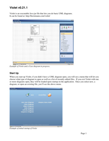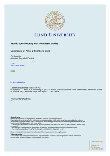
Transcription
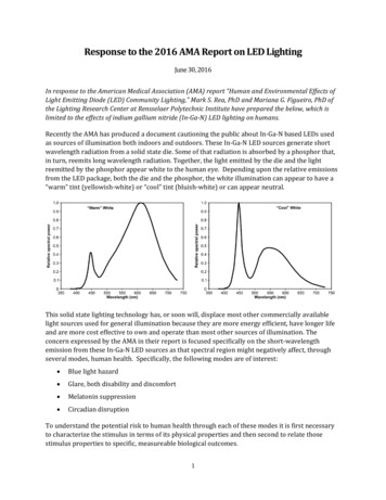
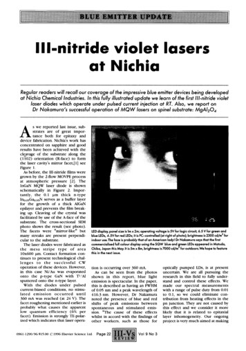
': ; ; r : . : . ; : : . t . : . . s. : :: : -:: :: . : : : . :: ,'. :: :: : : .: . :.: '.'-.:: : o .::::::::::::::::::::::::::::::::: :::. * :::.: : ,,::: ',.': : : * : ,,.' , o ! : ii : i:.! .: ! !. :. ii i . . . !. .b[, : : : : t . : : : . ;; ? . . :.-., : i i , , " : i , ' . ' # ; # : ' ' ;: * : ' t' : *;.:' % 1" : . . .:,' ; . , ' *, -*: ' : : ,.,:., . . ,:: . : .:., :. , . . : . .:::: : ii ,. :: : : *. :.: , . :o ' . . , %::o .: ' i#. :: : : !.':;.' : 4 '.:,:' %,, , , , ,,, ',' ,, tI I I - n i t r i d e v i o l e t lasersat NichiaRegular readers will recall our coverage of the impressive blue emitter devices being developedat Nichia Chemical Industries. In this fully illustrated update we learn of the first III-nitride violetlaser diodes which operate under pulsed current injection at RT. Also, we report onDr Nakamura's successful operation of M Q W lasers on spinel substrate: MgAI204s w e reported last issue, substrates are of great importance b o t h for epitaxy anddevice fabrication. Nichia's w o r k hasconcentrated on sapphire and goodresults have b e e n achieved with thecleavage of the substrate along the(1102) orientation (R-face) to formthe laser cavity's mirror facet,[1] seeFigure 1.As before, the III-nitride films w e r eg r o w n by the 2-flow MOVPE processat a t m o s p h e r i c p r e s s u r e [2]. TheInGaN MQW laser diode is s h o w nschematically in Figure 2. Importantly, t h e 0.1 tm t h i c k n - t y p eIno.osGao95N serves as a buffer layerfor the growth of a thick AIGaNepilayer and prevents the film breaking up. Cleaving of the crystal wasfacilitated by use of the A-face of thesubstrate. The cross-sectional SEMp h o t o shows the result (see photo).The facets w e r e "mirror-like" butmany streaks are present perpendicular to the substrate.The laser diodes w e r e fabricated asthe mesa stripe type of area10x600 tm. Contact formation continues to present technological challenges to the succ'essful CWoperation of these devices. However,in this case Ni/Au was evaporatedo n t o the p - t y p e GaN w i t h T ,/AIsputtered onto the n-type layer.With the d i o d e s u n d e r p u l s e dcurrent-biased conditions, no stimulated emission occurreduntil360 mA was reached (at 24 V). Thefacet roughening mentioned earlier isprobably what causes the apparentlow q u a n t u m efficiency (6% p e rfacet). Emission is strongly TE-polarized which indicates that laser opera-ALED displa) panel size is lm x 2m; operating voltage is 5V for logic circuit, 6.5 V for green andblue LEDs, 4.5V for red LEDs;it is PC-controlled (at right of photo); brightness is 2300 cd/m 2 forindoor use.The Face is probably that of an American lady! Dr Nakamura says that the firstcommercialised full colour display using the SQW blue and green LEDsappeared in Matudo,Chiba, Japan this May. It is 5m x 8m, brightness is 7000 cd/m For outdoors.We hope to featurethis in the next issue.tion is occurring over 360 mA.As can be seen from the photoss h o w n in this r e p o r t , blue lightemission is spectacular. In the paper,this is described as having an FXVHMof 0.05 nm and a peak wavelength of416.3 nm. However, Dr Nakamuranoted the p r e s e n c e of blue and redshifts of p e a k emissions b e t w e e ns p o n t a n e o u s and stimulated emission. "The cause of these effectswhilst in accord with the findings ofo t h e r workers, such as those for0961-1290/96/ 15.00 (t 1996 Elsevier Science Ltd. P a g e 22 I ] * , Vol g No 3optically p u m p e d LDs, is at presentuncertain. We are all pursuing theresearch in this field to fully understand and control these effects. Wemade our spectral measurementswith a range of pulse duty from 0.01to 0.1, so w e could eliminate contribution from heating effects in thepn junction, They are not caused bythis effect and w e consider it m o r elikely that it is related to epitaxiallayer inhomogeneity. Our ongoingproject is very m u c h aimed at making
;(i;)iii. ii 1.7i'i /' ! ?,,( iI;i,) )( 1 '-;t ;.I ';O )tll3fi! ii" !/ ! df! O" j IW jdl :ida xol!d:!,' !;( ;)Gid II !!XUJ.!CI I 'SVUl. qso9qSUl, dUl. svo9InlS () lOd ? al6u!s8V D 7V1 82 511117VI70 8170 111V783d17501 5 1V8158175 WOSJ
It0!i!i!i 0iiiiii 0iiii i!i! i!i i!ii0i i0i0iii0 0i!i0iii 0iii0 iiil i! !i!i i!0i010i010i iiii i 0 i iiii0iii it01 i 0 i0 0i0 ii 0iii0 ii i0 i i0 i iiii i 0i 0 i ! ii 0 i i0 ii0 i0i i ! ii i i 0: i : i i ii0i i: i ii ii! 0 i i ii0i i !ii! i iii0i0 i 0 ii ii iiii i 0 i iiii ii 0 iii0i0i 0 i0i ii iii0ithe epitaxy as well controlled aspossible of course. This has greatimportance but w e are making goodprogress".In the short history of blue emitterd e v e l o p m e n t it is sometimes convenient to not mention the temperature at which blue lasing action istaking place. What is very impressiveis Dr Nakamura's personal demonstration that his devices do actuallyw o r k at r o o m temperature. In thelatest w o r k lasing has b e e n measuredover the range 283 to 323K, i.e. wellabove RT. He notes that these laserdiodes have "characteristic temperatures (CT) of b e t w e e n 180 and 313K,typically 220K. ZnSe LDS had 150KCTs at RT. We are pleased with thisresult as w e n o w k n o w that our GaNbased devices are very stable even att e m p e r a t u r e s s o m e w h a t higher thanRT!"Last time, Dr Nakamura told TFRthat "We have b e e n using m a n ydifferent substrate types with no firmc o n c l u s i o n as to w h i c h has theoptimal characteristics. Sapphire hasb e e n successful but it has the majordrawback of being non-conductiveYThis n e c e s s i t a t e s s o m e ingeniousdevice fabrication p r o c e d u r e s especially for the formation of electricalcontacts.A n e w p a p e r describes some of thew o r k on alternative substrates currently underway at Nichia. In AppliedPhysics Letters [3] published in earlySEM photo of cleaved facet.Packaged LD:operating voltage20V; operatingcurrent 300mA; pulsewidth 1 ps; pulse priod1 ms; peak wavelength405 nm.April, reports MQW LDs grown on(1 t 1) MgAI204, a spinel, substrates isreported. As before, laser operationwas achieved, at 410 nm, u n d e rpulsed current conditions at RT.According to Dr Nakamura,apart from some subtle processadjustments basically the sameLT MOVPE epilayer g r o w t hconditions w e r e used. "Thecrystal quality of the GaN filmswas almost the same as that onsapphire. Our objective was totry to improve the roughness ofthe mirror facet and w e haveachieved this with a polishingt e c h n i q u e . This is in g o o da g r e e m e n t with the w o r k ofK u r a m a t a [4] w h o o b t a i n e dsmooth cleavage. But w e usedp o l i s h e d f a c e t s for t h e LDcavities. This gave a roughnessof around 50 angstroms afterthe polishing."]Basically similar device fabrication and contact informationw e r e used. However, high reflection facet coatings w e r ee m p l o y e d to h e l p r e d u c ethreshold current.Page 24. i! ii: : il::i i i::i::'Vol 9 No 3!iThis device did not lase until 1.2 Athreshold current was reached, at1.7A at 28 V. At 1.7 A the differentialq u a n t u m efficiency was 3.3% andpulsed output p o w e r was 44 m Wp e r facet, at 28 V. P h o t o g r a p h sclearly show strong blue emissionwith the spontaneous emissionspreading outwards when belowthreshold. Above threshold, stimulated emission occurs with a characteristic elliptical far-field pattern.Once again, Dr Nakamura and histeam at Nichia Chemical Industrieshave claimed a first for achieving bluelight laser emission for III-nitridebased devices on the MgAl20 4 substrate, hOur w o r k continues on theseand other substrates w h i c h w e h o p eto report in due course. I will bepleased to present our w o r k at theICMOVPE c o n f e r e n c e in Cardiff andalso the EMRS meeting in Strasbourg."Meanwhile, w e w i s h to d r a wattention to our LED w o r k w h i c hhas b e e n t h e basis of o u r lasersuccess. T h e full c o l o u r displays h o w n here, [see first page] incorporates III-nitride LED devices forthe blue and green emitters. These
You have to hand itto the designersof X ' Pert-M RDiii i
n-Ahn-ln0.cCaN btStructure of the InGaN MQW LD.2.4 A-face s a p p h i r e / /l "'. substrate/ / ' - ' : ' // //\ R-face576 ""' - L"" fGaNcleaved face (1100)[,/ C-faceGaN crystal60 Schematic of relationship between crystallographic orientation between (0001) c-face GaNfilm and (1120) A-face sapphire substrate.4303K293K 31 3K 3l !--K200References1. S. Nakamura, M. Senoh, S. Nagahama,N. Iwasa, T. Yamada, T. Matsushita, H.Kiyoku, Y. Sugimoto, InGaN MultiQuantum-Well-Structure Laser Diodeswith Cleaved Mirror Cavity Facets,Jpn. J. Appl. Phys. 35 (1996), pp. L217L220.2. S. Nakamura, Y. Harada and M. Senoh,Novel Metallorganic Chemical VapourDeposition System for GaN Growth,Appl. Phy. Lett. 58 (1991) 2101.J. Appl. Phys. Vol. 35 (1996), pp.L217-220.3. S. Nakamura, M. Senoh, S. Nagahama,N. Iwasa, T. Yamada, T. Matsushita, H.Kiyoku, Y. Sugimoto, InGaN multiquantum-well structure laser diodesgrown on MgAI204 substrates, Appl.Phys. Lett. 68 (15), 8 April 1996, pp2105-2107.4. Kuramata et al. Appl. Phys. Lett. 67(1995), 2521.Contact:810are InGaN and the r e d e l e m e n t s o n l yare GaAIAs. W e p r e p a r e d this as ad e m o n s t r a t i o n believing it is the firstfull c o l o u r display of this type to usethe SQW blue and g r e e n LEDs."I250I300IL350400]500450Current (mA)Temperature dependence of the L-I curve.Page 26I 1" Vol 9 No 3Dr S. N a k a m u r a ,Nichia Chemical Industries Ltd.,491 Oka K a m i n a k a ,Anan, Tokushima 774,Japan.Tel: [81] 884 22 2311.Fax: [81] 884 23 1802.E m a i h shuji@ nichia.co.jp
the laser cavity's mirror facet,[1] see Figure 1. As before, the III-nitride films were grown by the 2-flow MOVPE process at atmospheric pressure [2]. The InGaN MQW laser diode is shown schema