Transcription
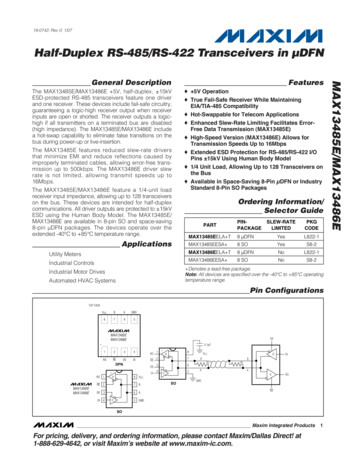
19-0742; Rev 0; 1/07Half-Duplex RS-485/RS-422 Transceivers in µDFNThe MAX13485E/MAX13486E 5V, half-duplex, 15kVESD-protected RS-485 transceivers feature one driverand one receiver. These devices include fail-safe circuitry,guaranteeing a logic-high receiver output when receiverinputs are open or shorted. The receiver outputs a logichigh if all transmitters on a terminated bus are disabled(high impedance). The MAX13485E/MAX13486E includea hot-swap capability to eliminate false transitions on thebus during power-up or live-insertion.The MAX13485E features reduced slew-rate driversthat minimize EMI and reduce reflections caused byimproperly terminated cables, allowing error-free transmission up to 500kbps. The MAX13486E driver slewrate is not limited, allowing transmit speeds up to16Mbps.The MAX13485E/MAX13486E feature a 1/4-unit loadreceiver input impedance, allowing up to 128 transceiverson the bus. These devices are intended for half-duplexcommunications. All driver outputs are protected to 15kVESD using the Human Body Model. The MAX13485E/MAX13486E are available in 8-pin SO and space-saving8-pin µDFN packages. The devices operate over theextended -40 C to 85 C temperature range.ApplicationsUtility MetersIndustrial ControlsFeatures 5V Operation True Fail-Safe Receiver While MaintainingEIA/TIA-485 Compatibility Hot-Swappable for Telecom Applications Enhanced Slew-Rate Limiting Facilitates ErrorFree Data Transmission (MAX13485E) High-Speed Version (MAX13486E) Allows forTransmission Speeds Up to 16Mbps Extended ESD Protection for RS-485/RS-422 I/OPins 15kV Using Human Body Model 1/4 Unit Load, Allowing Up to 128 Transceivers onthe Bus Available in Space-Saving 8-Pin μDFN or IndustryStandard 8-Pin SO PackagesOrdering Information/Selector EELA T8 µDFNYesL822-1MAX13485EESA 8 SOYesS8-2MAX13486EELA T8 µDFNNoL822-1MAX13486EESA 8 SONoS8-2 Denotes a lead-free package.Note: All devices are specified over the -40 C to 85 C operatingtemperature range.Industrial Motor DrivesAutomated HVAC SystemsPin ConfigurationsTOP VIEWVCCBAGND8765MAX13485EMAX13486EDE 0.1μF1234ROREDEDIRO ROMAX13485EMAX13486E18R27BDE36A5GNDD8R7DE 34DI65DVCCDBRtARSODIBRtAVCCREDI 4 2REDFN1ROGNDRESOMaxim Integrated ProductsFor pricing, delivery, and ordering information, please contact Maxim/Dallas Direct! at1-888-629-4642, or visit Maxim’s website at www.maxim-ic.com.1MAX13485E/MAX13486EGeneral Description
MAX13485E/MAX13486EHalf-Duplex RS-485/RS-422 Transceivers in µDFNABSOLUTE MAXIMUM RATINGS(All voltages referenced to GND.)VCC . 6VDE, RE, DI.-0.3V to 6VA, B .-8V to 13VShort-Circuit Duration (RO, A, B) to GND .ContinuousContinuous Power Dissipation (TA 70 C)8-Pin SO (derate 5.9mW/ C above 70 C).471mW8-Pin µDFN (derate 4.8mW/ C above 70 C) .380.6mWOperating Temperature Range .-40 C to 85 CJunction Temperature . 150 CStorage Temperature Range .-65 C to 150 CLead Temperature (soldering, 10s) . 300 CStresses beyond those listed under “Absolute Maximum Ratings” may cause permanent damage to the device. These are stress ratings only, and functionaloperation of the device at these or any other conditions beyond those indicated in the operational sections of the specifications is not implied. Exposure toabsolute maximum rating conditions for extended periods may affect device reliability.ELECTRICAL CHARACTERISTICS(VCC 5V 5%, TA TMIN to TMAX, unless otherwise noted. Typical values are at VCC 5V and TA 25 C.) (Notes 1, ferential Driver OutputVODRDIFF 100Ω, Figure 12.0RDIFF 54Ω, Figure 11.5VCCVNo loadVCC0.2V3V0.2VChange in Magnitude ofDifferential Output VoltageΔVODRDIFF 100Ω or 54Ω, Figure 1 (Note 3)Driver Common-Mode OutputVoltageVOCRDIFF 100Ω or 54Ω, Figure 1Change in Magnitude ofCommon-Mode VoltageΔVOCRDIFF 100Ω or 54Ω, Figure 1 (Note 3)VCC/2Input-High VoltageVIHDI, DE, REInput-Low VoltageVILDI, DE, RE0.8VInput CurrentIINDI, DE, RE 1µADriver Short-Circuit OutputCurrent (Note 4)IOSDDriver Short-Circuit FoldbackOutput Current Note 3)IOSDF2.0V0V VOUT 12V 50 250-7V VOUT 0V-250-50(VCC - 1V) VOUT 12V20-7V VOUT 0V-20mAmARECEIVERInput Current (A and B)IA, BDE GND, VCC GNDor 5VReceiver-Differential-ThresholdVoltageVTH-7V VCM 12VReceiver Input HysteresisΔVTHVA VB 0VOutput-High Voltage2VOHIO -1.6mA, VA - VB VTHVIN 12VVIN -7V250-200-200-5025VCC 1.5µAmVmVV
Half-Duplex RS-485/RS-422 Transceivers in µDFNELECTRICAL CHARACTERISTICS (continued)MAXUNITSOutput-Low VoltagePARAMETERSYMBOLVOLIO 1mA, VA - VB -VTHCONDITIONSMINTYP0.4VTri-State Output Current atReceiverIOZR0V VO VCC 1µAReceiver Input ResistanceRIN-7V VCM 12V48Receiver-Output Short-CircuitCurrentIOSR0V VRO VCC 7 95mA4.755.25VDE 1, RE 0, no load4.5mADE 0, RE 110µAkΩPOWER SUPPLYSupply VoltageVCCSupply CurrentICCShutdown Supply CurrentISHDNESD PROTECTIONESD Protection (A, B)Air Gap Discharge IEC61000-4-2(MAX13485E) 15Human Body Model 15ESD Protection (All Other Pins)Human Body Model 2kVkVSWITCHING CHARACTERISTICS—MAX13485E(VCC 5V 5%, TA TMIN to TMAX, unless otherwise noted. Typical values are at VCC 5V and TA 25 C.) (Note ver Propagation DelayDriver-Differential Output Rise orFall TimeDriver-Differential Output Skew tDPLH - tDPHL tDPLHtDPHLtHLtLHtDSKEWRDIFF 54Ω, CL 50pF, Figures 2 and 3RDIFF 54Ω, CL 50pF, Figures 2 and 320010002001000250900250900RDIFF 54Ω, CL 50pF, Figures 2 and 3Maximum Data Rate140500nsnsnskbpsDriver Enable to Output HightDZHFigures 4 and 52500nsDriver Enable to Output LowtDZLFigures 4 and 52500nsDriver Disable Time from HightDHZFigures 4 and 5100nsDriver Disable Time from LowtDLZFigures 4 and 5100nsDriver Enable from Shutdown toOutput HightDZH(SHDN) Figures 4 and 55500nsDriver Enable from Shutdown toOutput LowtDZL(SHDN) Figures 4 and 55500ns700nsTime to ShutdowntSHDN50340RECEIVERReceiver Propagation DelayReceiver Output SkewMaximum Data RatetRPLHtRPHLtRSKEW80CL 15pF, Figures 6 and 780CL 15pF, Figure 713500nsnskbps3MAX13485E/MAX13486E(VCC 5V 5%, TA TMIN to TMAX, unless otherwise noted. Typical values are at VCC 5V and TA 25 C.) (Notes 1, 2)
MAX13485E/MAX13486EHalf-Duplex RS-485/RS-422 Transceivers in µDFNSWITCHING CHARACTERISTICS—MAX13485E (continued)(VCC 5V 5%, TA TMIN to TMAX, unless otherwise noted. Typical values are at VCC 5V and TA 25 C.) (Note 1)PARAMETERMAXUNITStRZHFigure 850nsReceiver Enable to Output LowtRZLFigure 850nsReceiver Disable Time from HightRHZFigure 850nsReceiver Disable Time from LowtRLZFigure 850nsReceiver Enable to Output HighSYMBOLCONDITIONSMINTYPReceiver Enable from Shutdownto Output HightRZH(SHDN) Figure 82200nsReceiver Enable from Shutdownto Output LowtRZL(SHDN) Figure 82200ns700nsTime to ShutdowntSHDN50340SWITCHING CHARACTERISTICS—MAX13486E(VCC 5V 5%, TA TMIN to TMAX, unless otherwise noted. Typical values are at VCC 5V and TA 25 C.) (Note ver Propagation DelayDriver Differential Output Rise orFall TimeDifferential Driver Output Skew tDPLH - tDPHL tDPLHtDPHLtHLtLHtDSKEW50RDIFF 54Ω, CL 50pF, Figures 2 and 35015RDIFF 54Ω, CL 50pF, Figures 2 and 315RDIFF 54Ω, CL 50pF, Figures 2 and 3Maximum Data Rate816nsnsnsMbpsDriver Enable to Output HightDZHFigures 4 and 550nsDriver Enable to Output LowtDZLFigures 4 and 550nsDriver Disable Time from HightDHZFigures 4 and 550nsDriver Disable Time from LowtDLZFigures 4 and 550nsDriver Enable from Shutdown toOutput HightDZH(SHDN) Figures 4 and 52200nsDriver Enable from Shutdown toOutput LowtDZL(SHDN) Figures 4 and 52200ns700nsTime to ShutdowntSHDN50340RECEIVERReceiver Propagation DelayReceiver Output SkewMaximum Data Rate4tRPLHtRPHLtRSKEW80CL 15pF, Figures 6 and 780CL 15pF, Figure 71316nsnsMbps
Half-Duplex RS-485/RS-422 Transceivers in µDFN(VCC 5V 5%, TA TMIN to TMAX, unless otherwise noted. Typical values are at VCC 5V and TA 25 C.) (Note 1)PARAMETERSYMBOLCONDITIONSMINTYPMAXUNITSReceiver Enable to Output HightRZHFigure 850nsReceiver Enable to Output LowtRZLFigure 850nsReceiver Disable Time from HightRHZFigure 850nsReceiver Disable Time from LowtRLZFigure 850nsReceiver Enable from Shutdownto Output HightRZH(SHDN) Figure 82200nsReceiver Enable from Shutdownto Output LowtRZL(SHDN) Figure 82200ns700nsTime to ShutdowntSHDN50340Note 1: µDFN devices production tested at 25 C. Overtemperature limits are generated by design.Note 2: All currents into the device are positive. All currents out of the device are negative. All voltages referred to device ground,unless otherwise noted.Note 3: ΔVOD and ΔVOC are the changes in VOD and VOC when the DI input changes states.Note 4: The short-circuit output current applied to peak current just prior to foldback current limiting. The short-circuit foldbackoutput current applies during current limiting to allow a recovery from bus contention.Typical Operating Characteristics(VCC 5V, TA 25 C, unless otherwise noted.)OUTPUT CURRENT vs. RECEIVEROUTPUT HIGH VOLTAGE3.63.428211473.2-40-151035TEMPERATURE ( C)60855040302010003.060MAX13485-86E toc0335OUTPUT CURRENT (mA)SUPPLY CURRENT (mA)3.8OUTPUT CURRENT vs. RECEIVEROUTPUT LOW VOLTAGEMAX13485-86E toc02NO LOADOUTPUT CURRENT (mA)4.0MAX13485-86E toc01SUPPLY CURRENT vs. TEMPERATURE0123OUTPUT HIGH VOLTAGE (V)45012345OUTPUT LOW VOLTAGE (V)5MAX13485E/MAX13486ESWITCHING CHARACTERISTICS—MAX13486E (continued)
Typical Operating Characteristics (continued)(VCC 5V, TA 25 C, unless otherwise noted.)RECEIVER OUTPUT HIGHVOLTAGE vs. TEMPERATURE4.84.64.40.40.30.280MAX13485-86E toc06IO 1mAOUTPUT CURRENT (mA)5.0MAX13485-86E toc05OUTPUT HIGH VOLTAGE (V)5.2DIFFERENTIAL OUPUT CURRENTvs. DIFFERENTIAL OUTPUT VOLTAGE0.5OUTPUT LOW VOLTAGE (V)IO 1mARECEIVER OUTPUT LOWVOLTAGE vs. TEMPERATUREMAX13485-86E 3DRIVER-DIFFERENTIAL OUTPUTVOLTAGE vs. TEMPERATUREOUTPUT CURRENT vs. TRANSMITTEROUTPUT HIGH VOLTAGEOUTPUT CURRENT vs. TRANSMITTEROUTPUT LOW VOLTAGE1.51.00.58060401003560-7 -6 -5 -4 -3 -2 -1 08560400010802020-15MAX13485-86E toc09MAX13485-86E toc08100120OUTPUT CURRENT (mA)2.0120OUTPUT CURRENT (mA)2.5MAX13485-86E toc07OUTPUT VOLTAGE (V)0123450246810TEMPERATURE ( C)OUTPUT HIGH VOLTAGE (V)OUTPUT LOW VOLTAGE (V)SHUTDOWN CURRENTvs. TEMPERATUREDRIVER PROPAGATIONvs. TEMPERATURE (MAX13485E)DRIVER PROPAGATION DELAYvs. TEMPERATURE (MAX13486E)65432500tDPHL45040035012MAX13485-86E toc127tDPLH55030DRIVER PROPAGATION DELAY (ns)8600MAX13485-86E toc119DRIVER PROPAGATION DELAY (ns)MAX13485-86E URE ( C)654TEMPERATURE ( C)RDIFF 54Ω-401TEMPERATURE ( C)3.0DIFFERENTIAL OUTPUT VOLTAGE (V)00-40SHUTDOWN CURRENT (μA)MAX13485E/MAX13486EHalf-Duplex RS-485/RS-422 Transceivers in µDFN6085-40-151035TEMPERATURE ( C)6085-40-151035TEMPERATURE ( C)6085
Half-Duplex RS-485/RS-422 Transceivers in µDFNRECEIVER PROPAGATIONvs. TEMPERATURE (MAX13485E)tRPHL4020MAX13485-86E toc1460DRIVER PROPAGATION (500kbps)(MAX13485E)MAX13485/86E toc1540RECEIVER PROPAGATION (ns)MAX13485-86E toc13PROPAGATION DELAY (ns)80RECEIVER PROPAGATIONvs. TEMPERATURE 0-40-1510356085-40TEMPERATURE ( C)-1510356085400ns/divTEMPERATURE ( C)DRIVER PROPAGATION (16Mbps)(MAX13486E)RECEIVER PROPAGATION (16Mbps)(MAX13486E)MAX13485/86E toc16MAX13485/86E iv10ns/div7MAX13485E/MAX13486ETypical Operating Characteristics (continued)(VCC 5V, TA 25 C, unless otherwise noted.)
MAX13485E/MAX13486EHalf-Duplex RS-485/RS-422 Transceivers in µDFNTest Circuits and ure 2. Driver Timing Test CircuitFigure 1. Driver DC Test Loadf 1MHz, tLH 3ns, tHL 3nsVCCDI1.5V1.5V01/2 VOtDPHLtDPLHBA1/2 VOVOVDIFF V(A) - V(B)VOVDIFF90%90%010%10%-VOtHLtLHtDSKEW tDPLH - tDPHL Figure 3. Driver Propagation Delays8CL
Half-Duplex RS-485/RS-422 Transceivers in µDFNVCCDE1.5V1.5V0tDLZtDZL(SHDN),tDZLA, B2.3VVOL 0.5VOUTPUT NORMALLY LOWVOLOUTPUT NORMALLY HIGHA, B2.3VVOH 0.5V0tDZH(SHDN),tDZHtDHZFigure 4. Driver Enable and Disable Times500ΩS1VCCBOUTPUTUNDER TESTRVIDATECLRECEIVEROUTPUTAS2Figure 5. Driver-Enable and -Disable-Timing Test LoadFigure 6. Receiver Propagation Delay Test Circuitf 1MHz, tLH 3ns, tHL 3nsA1VB-1VtRPHLtRPLHVOHRO1.5VVOL1.5VtRSKEW tRPHL - tRPLH Figure 7. Receiver Propagation Delays9MAX13485E/MAX13486ETest Circuits and Waveforms (continued)
MAX13485E/MAX13486EHalf-Duplex RS-485/RS-422 Transceivers in µDFNPin DescriptionPINNAME1ROReceiver OutputFUNCTION2REReceiver Output Enable. Drive RE low to enable RO. RO is high impedance when RE is high. DriveRE high and DE low to enter low-power shutdown mode. RE is a hot-swap input (see the Hot-SwapCapability section for more details).3DEDriver Output Enable. Drive DE high to enable the driver outputs. These outputs are high-impedancewhen DE is low. Drive RE high and DE low to enter low-power shutdown mode. DE is a hot-swap input(see the Hot-Swap Capability section for more details).4DIDriver Input. Drive DI low to force noninverting output low and inverting output high. Drive DI high toforce noninverting output high and inverting output low (see the Function Tables).5GND6ANoninverting Receiver Input and Noninverting Driver Output7BInverting Receiver Input and Inverting Driver Output8VCCGroundPositive Supply, VCC 5V 5%. Bypass VCC to GND with a 0.1µF capacitor.Function HIGH IMPEDANCEHIGH X -50mV10X -200mV00XOPEN/SHORT111XHIGH IMPEDANCE10XSHUTDOWNX Don’t care, shutdown mode, driver, and receiver outputsare in high impedance.10
Half-Duplex RS-485/RS-422 Transceivers in µDFNS1 1VS3VCC1kΩ-1VVIDCL15pFGENERATORS250ΩS1 OPENS2 CLOSEDS3 1VS1 CLOSEDS2 OPENS3 -1VVCCVCCVCC/2VCC/2RERE00tRZH, tRZH(SHDN)tRZL, tRZL(SHDN)VOHROVCCVOH/2(VOL VCC)/2RO0S1 OPENS2 CLOSEDS3 1VVOLS1 CLOSEDS2 OPENS3 .25VFigure 8. Receiver Enable and Disable TimesVOLMAX13485E/MAX13486ETest Circuits and Waveforms (continued)
MAX13485E/MAX13486EHalf-Duplex RS-485/RS-422 Transceivers in µDFNDetailed DescriptionThe MAX13485E/MAX13486E half-duplex, high-speedtransceivers for RS-485/RS-422 communication containone driver and one receiver. These devices feature failsafe circuitry that guarantees a logic-high receiver output when receiver inputs are open or shorted, or whenthey are connected to a terminated transmission linewith all drivers disabled (see the Fail-Safe section). TheMAX13485E/MAX13486E also feature a hot-swap capability allowing line insertion without erroneous datatransfer (see the Hot-Swap Capability section). TheMAX13485E features reduced slew-rate drivers thatminimize EMI and reduce reflections caused byimproperly terminated cables, allowing error-free transmission up to 500kbps. The MAX13486E driver slewrate is not limited, making transmit speeds up to16Mbps possible.VCC10μsTIMERSR LATCHTIMER5kΩDE(HOT SWAP)DEFail-SafeThe MAX13485E/MAX13486E guarantee a logic-highreceiver output when the receiver inputs are shorted oropen, or when they are connected to a terminatedtransmission line with all drivers disabled. This is done bysetting the receiver input threshold between -50mV and-200mV. If the differential receiver input voltage (A - B) isgreater than or equal to -50mV, RO is logic-high. If (A - B)is less than or equal to -200mV, RO is logic-low. In thecase of a terminated bus with all transmitters disabled,the receiver’s differential input voltage is pulled to 0V bythe termination. With the receiver thresholds of theMAX13485E/MAX13486E, this results is a logic-high witha 50mV minimum noise margin. Unlike previous fail-safedevices, the -50mV to -200mV threshold complies withthe 200mV EIA/TIA-485 standard.Hot-Swap CapabilityHot-Swap InputsWhen circuit boards are inserted into a hot or poweredbackplane, differential disturbances to the data buscan lead to data errors. Upon initial circuit-board insertion, the data communication processor undergoes itsown power-up sequence. During this period, theprocessor’s logic-output drivers are high impedanceand are unable to drive the DE and RE inputs of thesedevices to a defined logic level. Leakage currents up to 10µA from the high impedance state of the processor’s logic drivers could cause standard CMOS enableinputs of a transceiver to drift to an incorrect logic level.Additionally, parasitic circuit-board capacitance couldcause coupling of VCC or GND to the enable inputs.Without the hot-swap capability, these factors couldimproperly enable the transceiver’s driver or receiver.12100μA500μAM1M2Figure 9. Simplified Structure of the Driver Enable Pin (DE)When VCC rises, an internal pulldown circuit holds DElow and RE high. After the initial power-up sequence,the pulldown circuit becomes transparent, resetting thehot-swap tolerable input.Hot-Swap Input CircuitryThe enable inputs feature hot-swap capability. At theinput there are two nMOS devices, M1 and M2 (Figure9). When VCC ramps from zero, an internal 7µs timerturns on M2 and sets the SR latch, which also turns onM1. Transistors M2, a 1.5mA current sink, and M1, a500µA current sink, pull DE to GND through a 5kΩresistor. M2 is designed to pull DE to the disabled stateagainst an external parasitic capacitance up to 100pFthat can drive DE high. After 7µs, the timer deactivatesM2 while M1 remains on, holding DE low against tristate leakages that can drive DE high. M1 remains onuntil an external source overcomes the required inputcurrent. At this time, the SR latch resets and M1 turnsoff. When M1 turns off, DE reverts to a standard highimpedance CMOS input. Whenever VCC drops below1V, the hot-swap input is reset.For RE there is a complementary circuit employing twopMOS devices pulling RE to VCC.
Half-Duplex RS-485/RS-422 Transceivers in µDFNCHARGE-CURRENTLIMIT RESISTORHIGHVOLTAGEDCSOURCECs100pFRC50MΩ TO 100MΩRD1500ΩCHARGE-CURRENTLIMIT APACITORFigure 10a. Human Body ESD Test ModelIP ACITORDEVICEUNDERTESTFigure 10c. IEC 61000-4-2 ESD Test ModelI100%90%PEAK-TO-PEAK RINGING(NOT DRAWN TO ERC1MΩAMPS36.8%10%010%0tRLTIMEtr 0.7ns TO 1nstDLCURRENT WAVEFORMFigure 10b. Human Body Current Waveform 15V ESD ProtectionAs with all Maxim devices, ESD-protection structuresare incorporated on all pins to protect against electrostatic discharges encountered during handling andassembly. The driver outputs and receiver inputs of theMAX13485E/MAX13486E have extra protection againststatic electricity. Maxim’s engineers have developedstate-of-the-art structures to protect these pins againstESD of 15kV without damage. The ESD structureswithstand high ESD in all states: normal operation, shutdown, and powered down. After an ESD event, theMAX13485E/MAX13486E keep working without latchupor damage.ESD protection can be tested in various ways. The transmitter outputs and receiver inputs of the MAX13485E/MAX13486E are characterized for protection to the following limits: 15kV using the Human Body Model 15kV using the Air Gap Discharge Method specifiedin IEC 61000-4-2 (MAX13485E only)t30ns60nsFigure 10d. IEC 61000-4-2 ESD Generator Current WaveformESD Test ConditionsESD performance depends on a variety of conditions.Contact Maxim for a reliability report that documentstest setup, test methodology, and test results.Human Body ModelFigure 10a shows the Human Body Model, and Figure10b shows the current waveform it generates when discharged into a low impedance. This model consists ofa 100pF capacitor charged to the ESD voltage of interest, which is then discharged into the test devicethrough a 1.5kΩ resistor.IEC 61000-4-2The IEC 61000-4-2 standard covers ESD testing andperformance of finished equipment. However, it doesnot specifically refer to integrated circuits. TheMAX13485E/MAX13486E help equipment designs tomeet IEC 61000-4-2, without the need for additionalESD-protection components.The major difference between tests done using theHuman Body Model and IEC 61000-4-2 is higher peakcurrent in IEC 61000-4-2 because series resistance islower in the IEC 61000-4-2 model. Hence, the ESD13
MAX13485E/MAX13486EHalf-Duplex RS-485/RS-422 Transceivers in OREDEROREDIDEROREFigure 11. Typical Half-Duplex RS-485 Networkwithstand voltage measured to IEC 61000-4-2 is generally lower than that measured using the Human BodyModel. Figure 10c shows the IEC 61000-4-2 model,and Figure 10d shows the current waveform for the IEC61000-4-2 ESD Contact Discharge test.Machine ModelThe machine model for ESD tests all pins using a 200pFstorage capacitor and zero discharge resistance.The objective is to emulate the stress caused when I/Opins are contacted by handling equipment during testand assembly. Of course, all pins require this protection, not just RS-485 inputs and outputs.The air-gap test involves approaching the device with acharged probe. The contact-discharge method connectsthe probe to the device before the probe is energized.Enable times tZH and tZL (see the Switching Characteristics) assume the devices were not in a low-power shutdown state. Enable times t ZH(SHDN) and t ZL(SHDN)assume the devices were in shutdown state. It takes drivers and receivers longer to become enabled from lowpower shutdown mode (tZH(SHDN), tZL(SHDN)) than fromdriver-/receiver-disable mode (tZH, tZL).Applications InformationLine Length128 Transceivers on the BusThe RS-485/RS-422 standard covers line lengths up to4000ft.The standard RS-485 receiver input impedance is 12kΩ(1-unit load), and the standard driver can drive up to32-unit loads. The MAX13485E/MAX13486E have a 1/4unit load receiver input impedance (48kΩ), allowing upto 128 transceivers to be connected in parallel on onecommunication line. Any combination of these devices,as well as other RS-485 transceivers with a total of 32unit loads or fewer, can be connected to the line.Reduced EMI and ReflectionsThe MAX13485E features reduced slew-rate driversthat minimize EMI and reduce reflections caused byimproperly terminated cables, allowing error-free datatransmission up to 500kbps.14Low-Power Shutdown ModeLow-power shutdown mode is initiated by bringing bothRE high and DE low. In shutdown, the devices draw amaximum of 10µA of supply current.RE and DE can be driven simultaneously. The devicesare guaranteed not to enter shutdown if RE is high andDE is low for less than 50ns. If the inputs are in thisstate for at least 700ns, the devices are guaranteed toenter shutdown.Typical ApplicationsThe MAX13485E/MAX13486E transceivers aredesigned for half-duplex, bidirectional data communications on multipoint bus transmission lines. Figure 11shows typical network applications circuits. To minimize reflections, terminate the line at both ends in itscharacteristic impedance, and keep stub lengths offthe main line as short as possible. The slew-rate-limitedMAX13485E is more tolerant of imperfect termination.Chip InformationPROCESS: BiCMOS
Half-Duplex RS-485/RS-422 Transceivers in 40.0140.0190.0070.0100.050 00.250.350.490.190.251.27 BSC3.804.005.806.200.40SOICN .EPSDIMAA1BCeEHL1.27VARIATIONS:1INCHESTOP IMETERSMIN4.808.559.80MAX5.008.7510.00N MS0128AA14AB16ACDABeC0 -8 A1LFRONT VIEWSIDE VIEWPROPRIETARY INFORMATIONTITLE:PACKAGE OUTLINE, .150" SOICAPPROVALDOCUMENT CONTROL NO.21-0041REV.B1115MAX13485E/MAX13486EPackage Information(The package drawing(s) in this data sheet may not reflect the most current specifications. For the latest package outline information,go to www.maxim-ic.com/packages.)
Package Information (continued)(The package drawing(s) in this data sheet may not reflect the most current specifications. For the latest package outline information,go to www.maxim-ic.com/packages.)ADXXXXXXXXXXXXbe6, 8, 10L UDFN.EPSMAX13485E/MAX13486EHalf-Duplex RS-485/RS-422 Transceivers in µDFNNSOLDERMASKCOVERAGEEPIN 10.10x45 LL11SAMPLEMARKINGPIN 1INDEX AREAAA(N/2 -1) x e)7CLCLbLAA2LeEVEN TERMINALA1eODD TERMINALPACKAGE OUTLINE,6, 8, 10L uDFN, 2x2x0.80 mm21-0164-DRAWING NOT TO SCALE-A12COMMON 5-2.052.050.500.10 REF.PACKAGE VARIATIONSPKG. CODENeb(N/2 -1) x eL622-160.65 BSC0.30 0.051.30 REF.L822-180.50 BSC0.25 0.051.50 REF.L1022-1100.40 BSC0.20 0.031.60 REF.PACKAGE OUTLINE,6, 8, 10L uDFN, 2x2x0.80 mm-DRAWING NOT TO SCALE-21-0164A22Maxim cannot assume responsibility for use of any circuitry other than circuitry entirely embodied in a Maxim product. No circuit patent licenses areimplied. Maxim reserves the right to change the circuitry and specifications without notice at any time.16 Maxim Integrated Products, 120 San Gabriel Drive, Sunnyvale, CA 94086 408-737-7600 2007 Maxim Integrated ProductsBobletis a registered trademark of Maxim Integrated Products, Inc.
General Description The MAX13485E/MAX13486E 5V, half-duplex, 15kV ESD-protected RS-485 transceivers feature one driver and