Transcription
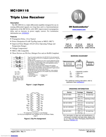
MC10H116Triple Line ReceiverDescriptionThe MC10H116 is a triple differential amplifier designed for use insensing differential signals over long lines and is a functional/pinoutduplication of the MC10116, with 100% improvement in propagationdelay and no increase in power supply current. For terminationinformation see AND8020.www.onsemi.comFeatures Propagation Delay, 1.0 ns Typical Power Dissipation 85 mW Typ/Pkg (same as MECL 10K ) Improved Noise Margin 150 mV (Over Operating Voltage and1 4253961071214131511VBB*VCC1 Pin 1VCC2 Pin 16VEE Pin 8When input pin withbubble goes positiveit’s respective outputpin with bubble goespositive.*VBB to be used to supply bias to the MC10H116 only and bypassed(when used) with 0.01ĂmF to 0.1 mF capacitor to ground (0 V). VBB cansource 1.0 mA.The MC10H116 is designed to be used in sensing differential signalsover long lines. The bias supply (VBB) is made available to make thedevice useful as a Schmitt trigger, or in other applications where astable reference voltage is necessary.Active current sources provide these receivers with excellentcommon mode noise rejection. If any amplifier in a package is notused, one input of that amplifier must be connected to VBB to preventunbalancing the current source bias network.The MC10H116 does not have internal input pull down resistors.This provides high impedance to the amplifier input and facilitatesdifferential connections.Applications: Low Level Receiver Voltage Level Schmitt TriggerInterface11PDIP 16P SUFFIXCASE 648 08Temperature Range)Voltage CompensatedMECL 10K CompatibleThese Devices are Pb-Free, Halogen Free and are RoHS Compliant162016PLCC 20FN SUFFIXCASE 775 02SOIC 16D SUFFIXCASE 751B 05MARKING YWW1610H116GAWLYWW1 Assembly Location Wafer Lot Year Work Week*For additional marking information, refer toApplication Note AND8002/D.Figure 1. Logic DiagramORDERING CINAIN512CINBOUT611VBBBOUT710BINVEE89BINPin assignment is for Dual in Line Package.For PLCC pin assignment, see TND309, the Pin Conversion Tables,page 9.Figure 2. Dip Pin Assignment Semiconductor Components Industries, LLC, 2016August, 2016 Rev. 11Downloaded from Arrow.com.1DevicePackageShipping†MC10H116DGSOIC 16(Pb-Free)48 Units/TubeMC10H116DR2GSOIC 16(Pb-Free)2500/Tape & ReelMC10H116FNGPLCC 20(Pb-Free)46 Units/TubeMC10H116FNR2GPLCC 20(Pb-Free)500/Tape & ReelMC10H116PGPDIP 16(Pb-Free)25 Units/Tube†For information on tape and reel specifications, including part orientation and tape sizes, please referto our Tape and Reel Packaging SpecificationsBrochure, BRD8011/D.Publication Order Number:MC10H116/D
MC10H116Table 1. MAXIMUM RATINGSSymbolRatingUnitVEEPower Supply (VCC 0)Characteristic 8.0 to 0VdcVIInput Voltage (VCC 0)0 to VEEVdcIoutOutput CurrentContinuousSurgeTAOperating Temperature RangeTstgStorage Temperature RangePlasticCeramicmA501000 to 75 C C 55 to 150 55 to 165Stresses exceeding those listed in the Maximum Ratings table may damage the device. If any of these limits are exceeded, device functionalityshould not be assumed, damage may occur and reliability may be affected.Table 2. ELECTRICAL CHARACTERISTICS (VEE 5.2 V 5%) (Note 2)0 Symbol75 MinMaxMinMaxMinMaxUnitPower Supply Current 23 21 23mAIinHInput Current High 150 95 95mAICBOInput Leakage Current 1.5 1.0 1.0mAVBBReference Voltage 1.38 1.27 1.35 1.25 1.31 1.19VdcVOHHigh Output Voltage 1.02 0.84 0.98 0.81 0.92 0.735VdcVOLLow Output Voltage 1.95 1.63 1.95 1.63 1.95 1.60VdcVIHHigh Input Voltage (Note 1) 1.17 0.84 1.13 0.81 1.07 0.735VdcVILLow Input Voltage (Note 1) 1.95 1.48 1.95 1.48 1.95 1.45Vdc 2.85 to 0.8 Vdc 150 typ mVPPIEVCMRVPPCharacteristic25 Common ModeRange (Note 4)Input Sensitivity (Note 3)1. When VBB is used as the reference voltage.2. Each MECL 10H series circuit has been designed to meet the specifications shown in the test table, after thermal equilibrium has beenestablished. The circuit is in a test socket or mounted on a printed circuit board and transverse air flow greater than 500 lfpm is maintained.Outputs are terminated through a 50 ohm resistor to 2.0 V.3. Differential input not to exceed 1.0 Vdc.4. 150 mVp p differential input required to obtain full logic swing on output.Table 3. AC CHARACTERISTICS0 Symbol75 MinMaxMinMaxMinMaxUnitPropagation Delay0.41.30.41.30.451.45nstrRise Time0.51.50.51.60.51.7nstfFall Time0.51.50.51.60.51.7nstpdCharacteristic25 NOTE: Device will meet the specifications after thermal equilibrium has been established when mounted in a test socket or printed circuitboard with maintained transverse airflow greater than 500 lfpm. Electrical parameters are guaranteed only over the declaredoperating temperature range. Functional operation of the device exceeding these conditions is not implied. Device specification limitvalues are applied individually under normal operating conditions and not valid simultaneously.MECL is a trademark of Semiconductor Components Industries, LLC (SCILLC) or its subsidiaries in the United States and/or other countries.www.onsemi.com2Downloaded from Arrow.com.
MECHANICAL CASE OUTLINEPACKAGE DIMENSIONSSOIC 16CASE 751B 05ISSUE KDATE 29 DEC 2006SCALE 1:1 A 16NOTES:1. DIMENSIONING AND TOLERANCING PER ANSIY14.5M, 1982.2. CONTROLLING DIMENSION: MILLIMETER.3. DIMENSIONS A AND B DO NOT INCLUDE MOLDPROTRUSION.4. MAXIMUM MOLD PROTRUSION 0.15 (0.006) PER SIDE.5. DIMENSION D DOES NOT INCLUDE DAMBARPROTRUSION. ALLOWABLE DAMBAR PROTRUSIONSHALL BE 0.127 (0.005) TOTAL IN EXCESS OF THE DDIMENSION AT MAXIMUM MATERIAL CONDITION.9 B 1P8 PL0.25 (0.010)8MBSGRKFX 45C T 10.003.804.001.351.750.350.490.401.251.27 .050 BSC0.0080.0090.0040.009070.2290.2440.0100.01916 PL0.25 (0.010)MT BSASSTYLE 1:PIN SEEMITTERNO NO E 2:PIN ENO CONNECTIONCATHODECATHODENO CONNECTIONANODECATHODECATHODEANODENO CONNECTIONCATHODECATHODENO CONNECTIONANODECATHODESTYLE 3:PIN 1.2.3.4.5.6.7.8.9.10.11.12.13.14.15.16.COLLECTOR, DYE #1BASE, #1EMITTER, #1COLLECTOR, #1COLLECTOR, #2BASE, #2EMITTER, #2COLLECTOR, #2COLLECTOR, #3BASE, #3EMITTER, #3COLLECTOR, #3COLLECTOR, #4BASE, #4EMITTER, #4COLLECTOR, #4STYLE 4:PIN 1.2.3.4.5.6.7.8.9.10.11.12.13.14.15.16.STYLE 5:PIN 1.2.3.4.5.6.7.8.9.10.11.12.13.14.15.16.DRAIN, DYE #1DRAIN, #1DRAIN, #2DRAIN, #2DRAIN, #3DRAIN, #3DRAIN, #4DRAIN, #4GATE, #4SOURCE, #4GATE, #3SOURCE, #3GATE, #2SOURCE, #2GATE, #1SOURCE, #1STYLE 6:PIN ANODEANODEANODEANODEANODEANODEANODESTYLE 7:PIN 1.2.3.4.5.6.7.8.9.10.11.12.13.14.15.16.SOURCE N‐CHCOMMON DRAIN (OUTPUT)COMMON DRAIN (OUTPUT)GATE P‐CHCOMMON DRAIN (OUTPUT)COMMON DRAIN (OUTPUT)COMMON DRAIN (OUTPUT)SOURCE P‐CHSOURCE P‐CHCOMMON DRAIN (OUTPUT)COMMON DRAIN (OUTPUT)COMMON DRAIN (OUTPUT)GATE N‐CHCOMMON DRAIN (OUTPUT)COMMON DRAIN (OUTPUT)SOURCE N‐CHCOLLECTOR, DYE #1COLLECTOR, #1COLLECTOR, #2COLLECTOR, #2COLLECTOR, #3COLLECTOR, #3COLLECTOR, #4COLLECTOR, #4BASE, #4EMITTER, #4BASE, #3EMITTER, #3BASE, #2EMITTER, #2BASE, #1EMITTER, #1SOLDERING ONS: MILLIMETERSDOCUMENT NUMBER:DESCRIPTION:98ASB42566BSOIC 16Electronic versions are uncontrolled except when accessed directly from the Document Repository.Printed versions are uncontrolled except when stamped “CONTROLLED COPY” in red.PAGE 1 OF 1ON Semiconductor andare trademarks of Semiconductor Components Industries, LLC dba ON Semiconductor or its subsidiaries in the United States and/or other countries.ON Semiconductor reserves the right to make changes without further notice to any products herein. ON Semiconductor makes no warranty, representation or guarantee regardingthe suitability of its products for any particular purpose, nor does ON Semiconductor assume any liability arising out of the application or use of any product or circuit, and specificallydisclaims any and all liability, including without limitation special, consequential or incidental damages. ON Semiconductor does not convey any license under its patent rights nor therights of others. Semiconductor Components Industries, LLC, 2019Downloaded from Arrow.com.www.onsemi.com
MECHANICAL CASE OUTLINEPACKAGE DIMENSIONS20 LEAD PLCCCASE 775 02ISSUE G20 1DATE 06 APR 2021SCALE 1:1B0.007 (0.180)Y BRK N MT L-M0.007 (0.180)UMNST L-MSG10.010 (0.250)SNSD L M ZW20D1XVST L-MSNSVIEW D DA0.007 (0.180)MT L-MSNSR0.007 (0.180)MT L-MSNSZCH T VIEW SG10.010 (0.250) S T L-MSEATINGPLANEDESCRIPTION:NSF0.007 (0.180)MT L-MSNSVIEW SSNSNOTES:1. DIMENSIONS AND TOLERANCING PER ANSI Y14.5M,1982.2. DIMENSIONS IN INCHES.3. DATUMS L , M , AND N DETERMINED WHERE TOPOF LEAD SHOULDER EXITS PLASTIC BODY AT MOLDPARTING LINE.4. DIMENSION G1, TRUE POSITION TO BE MEASURED ATDATUM T , SEATING PLANE.5. DIMENSIONS R AND U DO NOT INCLUDE MOLD FLASH.ALLOWABLE MOLD FLASH IS 0.010 (0.250) PER SIDE.6. DIMENSIONS IN THE PACKAGE TOP MAY BE SMALLERTHAN THE PACKAGE BOTTOM BY UP TO 0.012 (0.300).DIMENSIONS R AND U ARE DETERMINED AT THEOUTERMOST EXTREMES OF THE PLASTIC BODYEXCLUSIVE OF MOLD FLASH, TIE BAR BURRS, GATEBURRS AND INTERLEAD FLASH, BUT INCLUDING ANYMISMATCH BETWEEN THE TOP AND BOTTOM OF THEPLASTIC BODY.7. DIMENSION H DOES NOT INCLUDE DAMBARPROTRUSION OR INTRUSION. THE DAMBARPROTRUSION(S) SHALL NOT CAUSE THE H DIMENSIONTO BE GREATER THAN 0.037 (0.940). THE DAMBARINTRUSION(S) SHALL NOT CAUSE THE H DIMENSION TOBE SMALLER THAN 0.025 (0.635).DOCUMENT NUMBER:SK0.004 (0.100)JT L-MMK1EG0.007 (0.180)98ASB42594B20 LEAD PLCCGENERICMARKING 3950.3850.3950.1650.1800.0900.1100.0130.0210.050 BSC0.0260.0320.020 0.025 0.3500.3560.3500.3560.0420.0480.0420.0480.0420.056 0.0202100.3100.3300.040 90.330.531.27 BSC0.660.810.51 0.64 8.899.048.899.041.071.211.071.211.071.42 0.502107.888.381.02 1 20XXXXXXXXXXXXXXXXXGAWLYYWWXXXXXAWLYYWWG Specific Device Code Assembly Location Wafer Lot Year Work Week Pb Free Package*This information is generic. Please refer todevice data sheet for actual part marking.Pb Free indicator, “G” or microdot “ G”,may or may not be present.Electronic versions are uncontrolled except when accessed directly from the Document Repository.Printed versions are uncontrolled except when stamped “CONTROLLED COPY” in red.PAGE 1 OF 1ON Semiconductor andare trademarks of Semiconductor Components Industries, LLC dba ON Semiconductor or its subsidiaries in the United States and/or other countries.ON Semiconductor reserves the right to make changes without further notice to any products herein. ON Semiconductor makes no warranty, representation or guarantee regardingthe suitability of its products for any particular purpose, nor does ON Semiconductor assume any liability arising out of the application or use of any product or circuit, and specificallydisclaims any and all liability, including without limitation special, consequential or incidental damages. ON Semiconductor does not convey any license under its patent rights nor therights of others. Semiconductor Components Industries, LLC, 2019Downloaded from Arrow.com.www.onsemi.com
onsemi,, and other names, marks, and brands are registered and/or common law trademarks of Semiconductor Components Industries, LLC dba “onsemi” or its affiliatesand/or subsidiaries in the United States and/or other countries. onsemi owns the rights to a number of patents, trademarks, copyrights, trade secrets, and other intellectual property.A listing of onsemi’s product/patent coverage may be accessed at www.onsemi.com/site/pdf/Patent Marking.pdf. onsemi reserves the right to make changes at any time to anyproducts or information herein, without notice. The information herein is provided “as is” and onsemi makes no warranty, representation or guarantee regarding the accuracy of theinformation, product features, availability, functionality, or suitability of its products for any particular purpose, nor does onsemi assume any liability arising out of the application or useof any product or circuit, and specifically disclaims any and all liability, including without limitation special, consequential or incidental damages. Buyer is responsible for its productsand applications using onsemi products, including compliance with all laws, regulations and safety requirements or standards, regardless of any support or applications informationprovided by onsemi. “Typical” parameters which may be provided in onsemi data sheets and/or specifications can and do vary in different applications and actual performance mayvary over time. All operating parameters, including “Typicals” must be validated for each customer application by customer’s technical experts. onsemi does not convey any licenseunder any of its intellectual property rights nor the rights of others. onsemi products are not designed, intended, or authorized for use as a critical component in life support systemsor any FDA Class 3 medical devices or medical devices with a same or similar classification in a foreign jurisdiction or any devices intended for implantation in the human body. ShouldBuyer purchase or use onsemi products for any such unintended or unauthorized application, Buyer shall indemnify and hold onsemi and its officers, employees, subsidiaries, affiliates,and distributors harmless against all claims, costs, damages, and expenses, and reasonable attorney fees arising out of, directly or indirectly, any claim of personal injury or deathassociated with such unintended or unauthorized use, even if such claim alleges that onsemi was negligent regarding the design or manufacture of the part. onsemi is an EqualOpportunity/Affirmative Action Employer. This literature is subject to all applicable copyright laws and is not for resale in any manner.PUBLICATION ORDERING INFORMATIONLITERATURE FULFILLMENT:Email Requests to: orderlit@onsemi.comonsemi Website: www.onsemi.com Downloaded from Arrow.com.TECHNICAL SUPPORTNorth American Technical Support:Voice Mail: 1 800 282 9855 Toll Free USA/CanadaPhone: 011 421 33 790 2910Europe, Middle East and Africa Technical Support:Phone: 00421 33 790 2910For additional information, please contact your local Sales Representative
y14.5m, 1982. 2. controlling dimension: millimeter. 3. dimensions a and b do not include mold protrusion. 4. maximum mold protrusion 0.15 (0.006) per side. 5. dimension d does not include dambar protrusion. allowable dambar protrusion shall be 0.127 (0.005) total in excess of the d dimension