Transcription
9.7inch e-PaperVersion: 1.0TECHNICAL SPECIFICATIONMODEL NO: 9.7inch e-PaperThe content of this information is subject to be changed withoutnotice.Waveshare Electronicswebsite: https://www.waveshare.comAddr:10F, International Science & Technology Building, FuhongRd, Futian District, Shenzhen, ChinaI
9.7inch e-PaperRevision HistoryRev.1.0Issued Date2016-07-28Revised ContentsNewII
9.7inch e-PaperTECHNICAL SPECIFICATIONCONTENTS1.General Description .12.Features.13.Mechanical Specifications .14.Mechanical Drawing of EPD Module .25.Input / Output Interface .36.Display Module Electrical Characteristics .57.Power Sequence .108.Optical Characteristics .129.Handling, Safety and Environmental Requirements and Remark .1310.Reliability Test .1411.Border Definition.1512.Block Diagram.1613.Packing .17III
9.7inch e-Paper1.General Description9.7inch e-Paper is a reflective electrophoretic technology display module based on active matrix TFTsubstrate. It has 9.7” active area with 1200 x 825 pixels, the display is capable to display images at 2-16 graylevels (1-4 bits) depending on the display controller and the associated waveform file it used.2.Features High contrast reflective/electrophoretic technology 1200x825 display High reflectance Ultra wide viewing angle Ultra low power consumption Pure reflective mode Bi-stable Commercial temperature range Landscape, portrait mode Antiglare hard-coated front-surface3.Mechanical SpecificationsParameterSpecificationsUnitScreen Size9.7InchDisplay Resolution1200 (H) 825(V)PixelActive Area202.8 (H) 139.425 (V)mmPixel Pitch0.169 (H)x0.169 (V)mmPixel ConfigurationSquareOutline Dimension218.8(W) 156.425(H) 1.15(D)mmModule Weight80 8gNumber of Grey16 Grey Level (monochrome)Display operating modeReflective modeSurface treatmentAnti-glare treatment1Remark
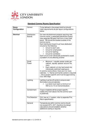
9.7inch e-Paper4.Mechanical Drawing of EPD Module9.7inch e-Paper2
9.7inch e-Paper5.Input / Output Interface5.1 Pin AssignmentIMSA-9637S-33Y905(IRISO)Pin #SignalDescriptionRemark1VNEGNegative power supply source driver-152NCNO Connection3VPOSPositive power supply source driver4NCNO Connection5VSSGround6NCNO Connection7VDDDigital power supply drivers8XCLClock source driver9XLELatch enable source driver10XOEOutput enable source driver11VDDDigital power supply drivers12XSTLStart pulse source driver13D0Data signal source driver14D1Data signal source driver15D2Data signal source driver16D3Data signal source driver17D4Data signal source driver18D5Data signal source driver19D6Data signal source driver20D7Data signal source driver21NCNO Connection22VCOMCommon voltage23NCNO Connection24VGHPositive power supply gate driver25NCNO Connection26VGLNegative power supply gate driver27NCNO Connection28MODE1Output mode selection gate driver29MODE1Output mode selection gate driver30VDDDigital power supply drivers31SPVStart pulse gate driver32CKVClock gate driver33BorderBorder connection3153.33.327-203.3
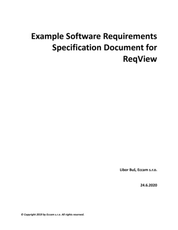
9.7inch e-Paper5.2 Panel Scan Direction4
9.7inch e-Paper6.Display Module Electrical Characteristics6.1 Absolute Maximum RatingParameterSymbolRatingUnitLogic Supply VoltageVDD-0.3 to 7VPositive Supply VoltageVPOS-0.3 to 18VNegative Supply VoltageVNEG 0.3 to -18VMax .Drive Voltage RangeVPOS - VNEG36VSupply VoltageVGH-0.3 to 45VSupply VoltageVGL-25.0 to 0.3VSupply RangeVGH-VGL-0.3 to 55VOperating Temp. RangeTOTR0 to 50 Storage TemperatureTSTG-25 to 70 Remark6.2 Display Module DC .3V-8000800mVVCOM-4Adjusted-0.3VICOM-0.43-mAPower PanelP--3980mWStandby Power PanelPSTBY--0.6mWParameterSymbolSignal GroundLogic Voltage SupplyGate Negative SupplyGate Positive supplySource Negative SupplySource Positive SupplyIDDVDD 3.3VVGLIGLVGL -20VVGHIGHVGH 27VVNEGINEGVNEG -15VVPOSIPOSBorder SupplyVCOMAsymmetry SourceVASMCommon VoltageConditionsVPOS 15VVPOS VNEG5
9.7inch e-Paper-The maximum power consumption is measured using 85Hz waveform with following pattern transition:from pattern of repeated 1 consecutive black scan lines followed by 1 consecutive white scan line to thatof repeated 1 consecutive white scan lines followed by 1 consecutive black scan lines (Note 6-1).-The Typical power consumption is measured using 85Hz waveform with following pattern transition: fromhorizontal 4 grey scale pattern to vertical 4 grey scale patterns (Note 6-2).-The standby power is the consumed power when the panel controller is in standby mode.-The listed electrical/optical characteristics are only guaranteed under the controller & waveform providedby manufactory-VCOM is recommended to be set in the range of assigned value 0.1V-The maximum ICOM inrush current is about 1.64 mANote6-1The maximum power consumptionNote6-2The typical power consumption6
9.7inch e-Paper6.3 Display Module AC k frequencyfckv--200kHzMinimum “L” clock pulse widthtwL0.5--usMinimum “H” clock pulse widthtwH0.5Clock rise timetrckv--100nsClock fall timetfckv--100nsSPV setup timetSU100--nsSPV hold timetH100--nsPulse rise timetrspv--100nsPulse fall timetfspv--100nsClock XCL cycle timetcy16.720-nsD0 . D7 setup timetsu8--nsD0 . D7 hold timeth8--nsXSTL setup timetstls8--nsXSTL hold timetstlh8--nsXLE on delay timetLEdly40--nsXLE high-level pulse width(When VDD 1.7V to 2.1V)tLEw40--nsXLE off delay timetLEoff200--nstout--12usOutput setting time to /- 30Mv(Cload 200pF)OUTPUT LATCH CONTROL SIGNALSOUT1 OUT12007us
9.7inch e-PaperCLOCK & DATA TIMINGCKV & SPV TIMINGGATE OUTPUT TIMINGNote:First gate line on timingAfter 5CKV, gate line is on.8
9.7inch e-Paper6.4 Refresh RateThe module is applied at a maximum screen refresh rate of 85Hz.Refresh RateMin.Max.-85Hz9
9.7inch e-Paper7.Power SequencePower rails must be sequenced in the following order:1. VSS VDD VNEG VPOS (Source driver) VCOM2. VSS VDD VGL VGH (Gate driver)POWER d100us-Ten0us-Tng1000us-Tgv100us-10
9.7inch e-PaperPOWER µs--Tne0µs--Ted0.5s-Discharged point @ -7.4 VoltNote 7-1: Supply voltages decay through pull-down resistors.Note 7-2: Begin to turn off VGL power after VNEG and VPOS are completely or almost discharged to GND state.Note 7-3: VGL must remain negative of VCOM during decay period.11
9.7inch e-Paper8.Optical Characteristics8.1 SpecificationsMeasurements are made with that the illumination is under an angle of 45 degrees, the detector is perpendicularunless otherwise specified.T ReflectanceWhite3342-%Note8-1GnNth Grey Level-L*-CRContrast Ratio-DS (WS-DS) n/(m-1)1016-WS: White state , DS: Dark state, Gray state from Dark to White :DS、G1、G2 、Gn 、Gm-2、WSm:4、8、16 when 2、3、4 bits modeNote 8-1: Luminance meter: Eye – One Pro Spectrophotometer8.2 Definition of contrast ratioThe contrast ratio (CR) is the ratio between the reflectance in a full white area (Rl) and the reflectance in a darkarea (Rd): CR Rl / Rd8.3 Reflection RatioThe reflection ratio is expressed as:R Reflectance Factorwhite board x ( Lcenter / Lwhite board )Lcenter is the luminance measured at center in a white area (R G B 1). Lwhite board is the luminance of a standardwhite board. Both are measured with equivalent illumination source. The viewing angle shall be no more than 2degrees.12-
9.7inch e-Paper9.Handling, Safety and Environmental Requirements and RemarkWarningThe display glass may break when it is dropped or bumped on a hard surface. Handle with care. Shouldthe display break, do not touch the electrophoretic material. In case of contact with electrophoreticmaterial, wash with water and soap.CautionThe display module should not be exposed to harmful gases, such as acid and alkali gases, which corrodeelectronic components.Disassembling the display module can cause permanent damage and invalidate the warranty agreements.IPA solvent can only be applied on active area and the back of a glass. For the rest part, it is not allowed.Mounting Precautions(1) It s recommended that you consider the mounting structure so that uneven force (ex. Twisted stress) isnot applied to the module.(2) It s recommended that you attach a transparent protective plate to the surface in order to protect theEPD. Transparent protective plate should have sufficient strength in order to resist external force.(3) You should adopt radiation structure to satisfy the temperature specification.(4) Acetic acid type and chlorine type materials for the cover case are not desirable because the formergenerates corrosive gas of attacking the PS at high temperature and the latter causes circuit break byelectro-chemical reaction.(5) Do not touch, push or rub the exposed PS with glass, tweezers or anything harder than HB pencil lead.And please do not rub with dust clothes with chemical treatment. Do not touch the surface of PS for barehand or greasy cloth. (Some cosmetics deteriorate the PS)(6) When the surface becomes dusty, please wipe gently with absorbent cotton or other soft materials likechamois soaks with petroleum benzene. Normal-hexane is recommended for cleaning the adhesives usedto attach the PS. Do not use acetone, toluene and alcohol because they cause chemical damage to the PS.(7) Wipe off saliva or water drops as soon as possible. Their long time contact with PS causesdeformations and color fading.Data sheet statusProduct specificationThis data sheet contains preliminary product specifications.Limiting valuesLimiting values given are in accordance with the Absolute Maximum Rating System (IEC 134). Stressabove one or more of the limiting values may cause permanent damage to the device. These are stressratings only and operation of the device at these or at any other conditions above those given in theCharacteristics sections of the specification is not implied. Exposure to limiting values for extendedperiods may affect device reliability.Application informationWhere application information is given, it is advisory and does not form part of the specification.RemarkAll The specifications listed in this document are guaranteed for module only. Post-assembled operationor component(s) may impact module performance or cause unexpected effect or damage and thereforelisted specifications is not warranted after any Post-assembled operation.13
9.7inch e-Paper10. Reliability TestTestHigh-Temperature1Operation2Low-Temperature Operation3High-Temperature Storage4Low-Temperature Storage5High-Temperature,High-Humidity Operation67ConditionMethodT 50 C, RH 30% for 240 hrsIEC 60 068-2-2BpT 0 C for 240 hrsIEC 60 068-2-2AbT 70 C, RH 23% for 240 hrs(Test In White Pattern)T -25 C for 240 hrs(Test In White Pattern)T 40 C, RH 90% for 168 hrsHigh Temperature,T 60 , RH 80% for 240hrsHigh- Humidity Storage(Test In White Pattern)Temperature Cycle-25 70 , 100 Cycles30mins 30 minsIEC 60 068-2-2BpIEC 60 068-2-1AbIEC 60 068-2-3CAIEC 60 068-2-3CAIEC 60 068-2-14(Test In White Pattern)8Solar Radiation Test765 W/m2 for 168hrs,40 (Test In White Pattern)IEC60 068-2-5Sa1.04G, Frequency: 10 500Hz9Package VibrationDirection: X,Y,ZFull packed for shipmentDuration: 1 hours in each directionDrop from height of 122 cm on concrete10Package Drop Impactsurface.Drop sequence: 1 corner, 3 edges, 6 facesfull packed for shipmentOne drop for each.11Electrostatic Effect(Machine model) /- 250V(non-operating)0Ω, 200pFPOLYACETAL Pen: Top R:0.8 mm12Stylus TappingLoad: 300gfSpeed: 2 times/secTotal 13,500times,IEC 62179, IEC 62180Test with bezel anddevice to simulate fullproduct testActual EMC level to be measured on customer application.Note:The protective film must be removed before temperature test.[Criteria]In the standard conditions, there is not display function NG issue occurred (Including: line defect, no image).All the cosmetic specification is judged before the reliability stress.14
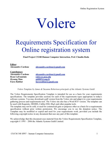
9.7inch e-Paper11. Border Definition15
9.7inch e-Paper12. Block Diagram16
9.7inch e-Paper13. Packing9.7inch e-Paper17
POS-0.3 to 18 V Negative Supply Voltage V NEG 0.3 to -18 V Max .Drive Voltage Range V POS - V NEG 36 V Supply Voltage V GH-0.3 to 45 V Supply Voltage V GL-25.0 to 0.3 V Supply Range V GH-V GL-0.3 to 55 V Operating Temp. Range T OTR 0 to 50 Storage


![[MS-ADTS-Diff]: Active Directory Technical Specification](/img/1/ms-adts-170316-diff.jpg)