Transcription
As originally published in the Pan Pacific Symposium Proceedings.ELECTROSTATIC DISCHARGE (ESD) – SOURCES OF ELECTROSTATICCHARGE IN A PRODUCTION LINE (SMT)Hartmut BerndtB.E.STAT European ESD competence centreKesslesdorf, Saxony, Germanyhberndt@bestat-esd.comABSTRACTThe number of failures caused by electrostatic discharges(ESD) has been increasing for some time now. So, it isnecessary for everyone, who handles electrostaticsensitive devices (ESDS), to know the reasons of suchfailures. This presentation will give an overview aboutpossible causes for ESD in a SMT production line.Particularly automated production lines have someprocessing steps, where electrostatic charges areincreasingly generated. So far one has been focused on thehuman being. This is controllable. Measurements inproduction lines show electrostatic charges at thefollowing processing steps: application of soldering paste(printer), assembling (automated and manual pick andplace), and labelling as well as optical and electrical tests(ICT). The electronic components are always assembleddirectly and without any covering on the PCBs. Thus, thewire bonding process leads to a damage of the electroniccomponents. This process step is a very critical part in theproduction line. The electronic devices will be directlycontacted with a metal needle.The process steps, where the PCBs are covered withenclosures must be inspected either. Such enclosures aremostly made of isolating materials, like plastics. Thus,those can be electrostatic charged highly, whileassembling.An optimized ESD Control System for machines with theemphasis on cost-effectiveness will be presented.Key words:Automation SMT production lineAutomation handling equipmentElectrostatic dischargeESD Control SystemProduct qualityINTRODUCTIONAll electronic components and assemblies are to be at riskof electrostatic discharges. Producers, suppliers,distributors and users have to realize the ESD controlsystem during the whole manufacturing process, duringthe measurements as well as during the application. Allactive electronic components, beginning with simplediodes, transistors or complex inner circuits, require anextern ESD control system. In the next step, SMDresistors and condensers, and prospectively NEMS andMEMS will be included in this danger category. Testsshow, that these passive components can be damagedthrough electrostatic discharges.The structures of electronic components become smaller.Already 5 volts of an electrostatic charge are enough tochange the structures in small electronic components. Thestructures will achieve such small dimensions, soelectrostatic charges can cause permanent damages. In theyear 2022 the sizes of the electronic components will beless than 10 nm. Electrostatic charges of 0,1 nC andelectrostatic fields of 10 V/cm will be enough then todamage ESDS permanently.PROCESS STEPS IN A SMT PRODUCTION LINEEvery time PCBs are handled, electrostatic charges aregenerated. A SMT production line has different processsteps, where such charges may be generated. As a matterof principle a PCB can always be charged by anymovements. The isolating plastic, which is used as basicmaterial, is mostly the main reason. The material iselectrostatically charged by friction, p. e. by conveyorbelts, although these are mostly made of conductivematerial.Soldering PrintingOne of these processes is the so called soldering printingof PCBs with soldering paste. This procedure and thefollowing slitting process PCB - printing colander leads tohigh charges. This would not be critical, unless ESDSexist on PCBs. Usually PCBs are assembled on bothsides. That means that electronic components alreadyexist during the second print or the backside-print. Veryhigh electrostatic charges may arise while separating theprinting colander from the PCB. This slitting process istypical example for the generation of electrostatic charges.It does not matter if the colander is made of metal orplastic.
As originally published in the Pan Pacific Symposium Proceedings.AOIAfterwards an optical/vision inspection, so called AOI,follows. This process does not generate any electrostaticcharges by itself, but the transportation does.Optical test procedures are probably the only processes,which do not cause any electrostatic charges.Pick-and-Place MachineThe PCBs arrive at the machine, which is electrostaticallycharged on the surface. Now a charge exchange happensinside the machine. Electronic components areelectrostatically charged and are assembled with the PCB.The PCB is charged either. While placing the ESDS onthe PCB the charge exchange takes place. This dischargecurrent damages the ESDS.Electronic components/ESDS are charged through theprocess „removing them from a tray or blister“.Electrostatic charges are generated during this slittingprocess. The ESDS are picked by the placement head andplaced on the several PCBs. In the past one hadexperienced with the material of such placement head.Nevertheless, electrostatic charges cannot be avoided oreven discharged by these. The reason therefore is theESDS’ enclosure, which is generally made of plastic(isolating).ICTPCBs may be electrostatically charged during thetransport between two process steps. The following ICT(integrated circuit test machine) leads to a suddendischarge of the existing electrostatic charges on the PCBor on the single electronic component. The reasontherefore is the direct contact of the metal needle(measurement probe) with the component’s pins. A seriesresistor would not be any solution, because the dischargehappens directly at the contact point between needle andpin.Assembly ProcessesDifferent assembly processes cause the contact ofisolating enclosure parts with static control sensitivecomponents. Thus, an influence of the ESDS happens bythe electrostatic field of isolating plastic parts. A chargetransfer on the ESDS effected, which probably can causedischarges during the production process or at thecustomer.Wire Bonding ProcessA very critical process is the wire bonding process, duringthe handling of ESDS (naked chips) as well as during thewire bonding of whole assemblies. Mostly, PCBs areelectrostatically charged by the enclosures or through thetransport process. During the wire bonding process adirect contact between a metal needle and an ESDS occursagain. Thus, a sudden discharge is provoked and theESDS is damaged.Further ProcessesLabeling processes, transport machines or systems,cutting systems or other steps can produce electrostaticpotential differences. These differences can damageelectronic parts: Isolating parts: plastic glass, plastic covers Pneumatic lines and cables: rubber transportationsystem, plastic rolls Anodized surfaces: aluminum Pick-up mechanisms: nozzles Vacuum cups GrippersFAILURE MODELS (CDM, CBM UND FICBM)Different failure models are used for the analyses ofhumans and machines. The HBM (Human Body Model) isalways used for the electrostatic charge of a person.Otherwise the CDM (Charged Device Model) is appliedfor the charge analysis of machines or production lines.Nevertheless, both will not be sufficient in the future.New failure models like the CBM (Charged Board Model)or the FICBM (Field Induce Charged Board Model)become necessary. The CDM only considers a singleelectronic component; however the CBM is applied toanalyze the whole PWB.Reflecting the following considerations, single failuremodels are caused: A person touches an electronic component and thestored electrostatic charges are transported from theperson to the electronic component. These charges aregrounded by the connection between the electroniccomponent and the earth potential. An electronic component or an electronic device actsas capacitor plate and stores electrostatic charges.While contacting the earth potential, damages arecaused by a discharge pulse. A charged object is in an electric field. A potential isgenerate over the gateoxid or the pn-junction of anelectronic component. Electrostatic charges are
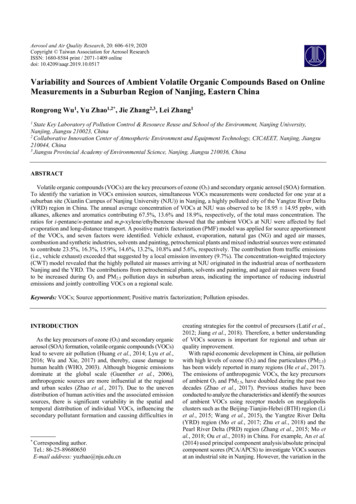
As originally published in the Pan Pacific Symposium Proceedings.generated and discharges cause damages (breakdown).Already known failure models: HBM (Human Body Model) MM (Machine Model) CDM (Charged Device Model) FIM (Field Induced Model)enough to bring the electronic component in the near of adischargeable point or object. So, an electrical orelectrostatic field may already provoke such a discharge.Damages of pn-junction, dielectric and other componentsare caused by a discharge impulse and its dischargecurrent, depending on the grounding via the enclosure orthe chip.The first failure model only considers the charged person.The second one is a specialization of the HBM (HumanBody Model). The third failure model assumes that theelectronic component charges itself electrostatically anddischarges itself suddenly by contacting metal. However,a person does not influence directly the charge anddischarge process any more at this third one.Reflecting the fact that quick discharges must beconsidered more and more in the future, all statementsabout electrostatic charges so far won’t be sufficient anymore. Very fast discharges in very short terms alreadyexist. Those are really energy loaded and damage ESDSof course.Nowadays, it is not enough to consider every singleelectronic component. One has to analyze the completeelectronic assembly either. However, a suitable failuremodel is still missing. Two models are in preparation: theCBM (Charged Board Model) and the FICBM (FieldInduce Charged Board Model). Both assume that theboard (PWB) is electrostatic charged. The board has ahigher capacity, so that it may store much moreelectrostatic charges. Those can also be grounded by asingle electronic component. The high energy causes anearly damage of the whole electronic component.Charged Device Model (CDM)The electronic component acts as a condenser. It gatherscharges, such caused while sliding through a magazine orwhile contacting another charged object. Additionally,electrostatic charges are generated by removing theelectronic component from a conductive tray or a belt.Electrostatic charges are generally caused by taking anelectronic component out of conductive material, becauseit is not equipped with a conductive enclosure. Thus, anelectronic component is always electrostatic charged afterevery mechanical process, independent of its actualhandling like the movement in a pick-and-place-machineor another production line. However, just only a dischargedamages the electronic component. The discharge can berealized directly or indirectly via further processes. It justPicture 1 Typical CDM dischargeAn electronic component can store energies up to 100 J.However, at a very low contact resistance ( m ) and aconduction inductivity of 10 nH, such energy, dependingon the charge amount, can realize a direct or an indirectconnection to the earth potential. An output per impulse ofseveral 100 W to 1000 W is reached by an increase of thedischarge current impulse of several ns. Such outputs areenough to change the component parameters considerablyor to destroy the electronic component finally (seeWunsch und Bell [6]).Charged Board Model (CBM)The previous models HBM and CDM are not enough todescribe ESD failures. There will be almost breakdownscaused by humans, but the most ESDS are moved inautomatically handling equipments. There is no directinfluence of the human. The electronic components andassemblies charge themselves electrostatic. The capacityconditions of a PWB are absolute different in comparisonto humans. That’s why one has been searched for a newmodel for some years because of starting with newconditions. One solution is the charged board model(CBM). Here the capacity proportions are very difficult.The value of the capacity is higher as the body of theperson. The result is a bigger electrostatic charge on theboard. We have a bigger energy at the discharge. Thisleads to the influence of ESDS and it damages the ESDS.
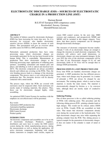
As originally published in the Pan Pacific Symposium Proceedings.discharge pointsingle electronic devicegrounded platePWBPicture 2 Typical CBM dischargeField Induce Charged Board Model (FICBM)A different model is the FICBM. The influence of theelectrical field on PCBs has been neglected or has beenthought that it is not important, until now. An electricalfield is able to produce electrostatic charges on a PCB,like demonstrated. These electrostatic charges will bestored by the bigger capacity of the PCB or by theelectronic components on it. The discharge process is notpredictable. It can always happen, when the PCB isgrounded or contacted. That’s why the description ofFICBM is not easy, but the effect is very important.Electrical fields can appear everywhere, where machines,motorized plants stand or where circuit processes areproduced.STEPS FOR THE MACHINE GROUNDINGThe first and only requirements are the demand for agrounding of all metal parts as well as the demand for theavoidance of plastic usage, which could generateelectrostatic charges and fields. He experiences show, thatit is not enough for the protection of ESDS in automatedmachines and systems. ESDS won’t be damaged by theoperator, but through the machines. The transportoperation of an ESDS in a machine can happen asfollowing:These examples show, that electrostatic charges alwaysdevelop, when ESDS are parted or moved. Electrostaticcharges will always generate because of the reason, whichthe components as well as the PWBs are made of anisolating material. Other acts and production steps show,that this is not the only possibility for the generation ofelectrostatic charges in a production process. Furthercritical steps are for example: the printing of PWBs, thelabeling of PWBs and assemblies as well as testconstructions.Manual handling of individual components is not commonanymore. PWB assemblies are handled mainly byequipment and the final phases of mechanical assemblyare done by both humans and robots. In consequence ofthis the Human Body Model (HBM) is not valid ESDsimulation model as much as previous. The mainelectrostatic risk during automated manufacturing is withCharged Device Model (CDM) type of electrostaticdischarges. The additional model, but not standardized yetis Charged Board Model (CBM).In the CBM type of ESD the assembled Printed WiringBoard (PWB) or some of the mechanics parts can becharged during handling and the discharge to ground orbetween the objects can happen. CBM type of discharge istypically more severe than other models for componentsdue to high capacitance and high stored charge of PWBassemblies or mechanics. There are some main ESDcontrol principles which are important in ESD ProtectedArea (EPA) as well as in automated process equipment:1. All conductive and dissipative items are grounded.1. Removal of the ESDS out of packaging. This is thefirst partition act. The ESDS has an isolating case, soit will be electrostatic charged during the removalout of the reel or the tray.2. Materials or parts to be contacted with ESDS aremade of electrostatic dissipative material.2. The electrostatic charged ESDS will be transportedto the PWB. Thereby a further electrostatic chargecan happen. The movement at High speed Pick-andPlace System should be enough of the generation ofelectrostatic charges.4. Where insulating materials or parts are needed, thepossible charges shall be minimized by specialmeasures, like ionization, shielding or coating.3. Through the placing on the PWB, different potentialbetween the ESDS and the PWB exist. So thepotential difference leads to a discharge, which willdamage the ESDS.3. Non-essential insulating materials are excluded.Enclosures of machines are normally made of conductivematerial. The conductive enclosure should have a straightand reliable connection to ground and the distance of theinsulating parts should be long enough in order not tocreate high electrostatic fields close to ESDS. Specialattention should be paid for grounding of parts which areseparated from the enclosure or are movable, likeadjustable conveyor.
As originally published in the Pan Pacific Symposium Proceedings.Type ofmeasurementResistance toground(only metalparts)Point-to-pointresistance orsurfaceresistanceElectrostaticpotential orelectrostaticvoltageElectrostaticfieldESD itemLimits1equipmentbody(enclosure)moving partsall surfaces, incontact withthe ESDSAll surfaces,in contactwith theESDSConductiveparts ofequipmentSurfaces incontact withESDS itemsor closer than15 cm of themESDS, PWBandmechanicalparts 3ESDS, PWBandmechanicalparts 2,3ESDS andPWBassemblies 3RG 2 R G 106 106 R G 109 106 R G 109 V 5 voltsmade of electrostatic dissipative material at least incontact area and a resistance to ground value shall bebetween 106 and 109 .Components and PWB material have plastic, insulatingmaterial and they can become charged by tribocharging,e.g. by rubbing against conveyor belt, touching on otherproduct parts or in routing process. The charged ESDSitem can subject to CDM or CBM risk. All rotating andsliding elements form an ESD risk. The tribochargingduring automated manufacturing shall be minimized andmetal contact to ESDS shall be prevented. Normally it isnot enough, an ionizer shell be installed in the area ofrotating material.V 50 voltsIonizers are applied sometimes to remove electrostaticcharges from machines. Electronic components and PWBscannot be grounded. Thus, ionization is the only methodminimizing electrostatic charges at the moment.V 100 voltsIonization is just one opportunity decreasing electrostaticcharges. Intelligent ionizers are able to detect electrostaticcharges in machines and to generate equivalent chargesfor their decrease either. The limits are shown in table 1.electrostatic fieldstrength 10000 volts/mmeasured at theposition of ESDS orelectrostatic chargeQ 5 10-9CoulombTable 1 Requirements for AHE (automated handlingequipments) [4]1Electrostatic potential, field and charge values areabsolute values, so they can have either positive ornegative readings.2If the potential of process essential insulators exceeds2000 volts the item must be kept a minimum of 30 cmfrom ESDS.3Stored charges should be less than required to causeCDM or CBM type of damage for the device.There are a lot of materials which can be in contact withESDS items. Components to be placed are stored in reelswith plastic tapes covered and nozzle picks the componentfrom reel. Components are placed on the PWB and PWBis contacted with conveyor belts and possible supportpins, gripper, clamps etc. All these materials should beThe mentioned ESD control steps are in common with thetoday’s knowledge.MEASUREMENT METHODS AND RESULTSThe following measurements are recommended toperform in order to evaluate the capability of automatedequipment:1.2.3.4.5.6.Resistance to groundPoint to point resistanceElectrostatic potentialElectrostatic fieldAccumulated chargeEMI (Electromagnetic Interference)Resistance to ground measurement is one of the mostimportant measurements in automated equipment. Eachindividual part is measured, like equipment body,conveyor reel, gripper, nozzle, jig, support table/pins etc.In additional to this point-to-point or surface resistancehave to measure from all surfaces which take a contactwith ESDS items. The appropriate probes can be used.Electrostatic potential is measured from ESDS and PWBassemblies by qualified meter. Electrostatic field ismeasured from insulating materials according to
As originally published in the Pan Pacific Symposium Proceedings.manufacturer’s instructions of meter. The largeconductive and grounded area can affect to themeasurements of potential and field.For evaluation of real ESD risk in automated processes,the handled ESD sensitive devices or products have to beanalyzed when production is ongoing. The methods are tomeasure the potential and charge of the devices. Thecharge can be measured by individual charge meter or bymeasuring th
ESD Control System . Product quality . INTRODUCTION . All electronic components and assemblies are to be at risk of electrostatic discharges. Producers, suppliers, distributors and users have to realize the ESD control system during the whole manufacturing process, durin