Transcription
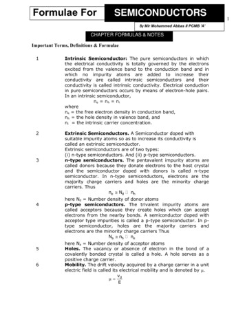
uFormulae ForSEMICONDUCTORS11 11By Mir Mohammed Abbas II PCMB 'A'CHAPTER FORMULAS & NOTESImportant Terms, Definitions & Formulae1Intrinsic Semiconductor: The pure semiconductors in whichthe electrical conductivity is totally governed by the electronsexcited from the valence band to the conduction band and inwhich no impurity atoms are added to increase theirconductivity are called intrinsic semiconductors and theirconductivity is called intrinsic conductivity. Electrical conductionin pure semiconductors occurs by means of electron-hole pairs.In an intrinsic semiconductor,ne nh niwherene the free electron density in conduction band,nh the hole density in valence band, andni the intrinsic carrier concentration.2Extrinsic Semiconductors. A Semiconductor doped withsuitable impurity atoms so as to increase its conductivity iscalled an extrinsic semiconductor.Extrinsic semiconductors are of two types:(i) n-type semiconductors. And (ii) p-type semiconductors.n-type semiconductors. The pentavalent impurity atoms arecalled donors because they donate electrons to the host crystaland the semiconductor doped with donors is called n-typesemiconductor. In n-type semiconductors, electrons are themajority charge carriers and holes are the minority chargecarriers. Thusne Nd nh3456here Nd Number density of donor atomsp-type semiconductors. The trivalent impurity atoms arecalled acceptors because they create holes which can acceptelectrons from the nearby bonds. A semiconductor doped withacceptor type impurities is called a p-type semiconductor. In ptype semiconductor, holes are the majority carriers andelectrons are the minority charge carriers ThusNa nh nehere Na Number density of acceptor atomsHoles. The vacancy or absence of electron in the bond of acovalently bonded crystal is called a hole. A hole serves as apositive charge carrier.Mobility. The drift velocity acquired by a charge carrier in a unitelectric field is called its electrical mobility and is denoted by .v dE1
CHAPTER FORMULAS & NOTESThe mobility of an electron in the conduction band is greaterthan that of the hole (or electron) in the valence band.78910Electrical conductivity of a Semiconductor. If a potentialdifference V is applied across a conductor of length L and areaof cross-section A, then the total current I through it is given byI eA (neve nh vh)where ne and nh are the electron and hole densities, and ve andvh are their drift velocities, respectively. If h are the electronand hole mobilities, then the conductivity of the semiconductorwill be e (ne e nh h)1and the resistivity will be e(ne e nh h )The conductivity of an intrinsic semiconductor increasesexponentially with temperature asEg 0 exp 2kB T Forward and Reverse Biasing of a pn-junction. If thepositive terminal of a battery is connected to the p-side and thenegative terminal to the n-side, then the pn-junction is said tobe forward biased. Both electrons and holes move towards thejunction. A current, called forward current, flows across thejunction. Thus a pn-junction offers a low resistance when it isforward biased.If the positive terminal of a battery is connected to the n-sideand negative terminal to the p-side, then pn-junction is said tobe reverse biased. The majority charge carriers move away fromthe junction. The potential barrier offers high resistance duringthe reverse bias. However, due to the minority charge carriers asmall current, called reverse or leakage current flows in theopposite direction.Thus junction diode has almost a unidirectional flow of current.Action of a transistor. When the emitter-base junction of annpn-transistor is forward biased, the electrons are pushedtowards the base. As the base region is very thin and lightlydoped, most of the electrons cross over to the reverse biasedcollector. Since few electrons and holes always recombine in thebase region, so the collector current Ic is always slightly lessthen emitter current IE.IE IC IBwhere IB is the base current.Three Configurations of a Transistor. A transistor can beused in one of the following three configurations:(i)Common-base (CB) circuit.(ii)Common-emitter (CE) circuit.2
CHAPTER FORMULAS & NOTES112(iii)Common-collector (CC) circuit.Current Gains of a Transistor. Usually low current gains aredefined:(i)Common base current amplification factor or accurrent gain . It is the ratio of the small change in thecollector current to the small change in the emitter currentwhenthecollector-basevoltageiskeptconstant. I C IE V cons tan tCB(ii) Common emitter current amplification factor or accurrent gain . It is the ratio of the small change in thecollector current to the small change in the base current whenthe collector emitter voltage is kept constant. I C IB V cons tantCE1213Relations between and . The current gains and arerelated as and 1 1 Transistor as an amplifier. An amplifier is a circuit which isused for increasing the voltage, current or power of alternatingform. A transistor can be used as an amplifier.ac current gain is defined as: I ac or Ai C IB V cons tan tCEdc current gain is defined as I dc C IB VCE cons tan tVoltage gain of an amplifier is defined asVA small change in output voltageAv o ViA small change in input voltage VCE VBEOrA v ac.R out Ai. ArRini.e., Voltage gain Current gain Resistance gainPower gain of an amplifier is defined asOutpur powerAp Current Voltage gainInput power
CHAPTER FORMULAS & NOTESOrAp Ai.A v 2ac.141516171819202122R outRinLogic Gate. A logic gate is a digital circuit that has one or moreinputs but only one output. It follows a logical relationshipbetween input and output voltage.Truth Table. This table shows all possible input combinationand the corresponding output for a logic gate.Boolean Expression. It is a shorthand method of describingthe function of a logic gate in the form of an equation or anexpression. It also relates all possible combination of the inputsof a logic gate to the corresponding outputs.Positive and Negative Logic. If in a system, the highervoltage level represents 1 and the lower voltage level represent0, the system is called a positive logic. If the higher voltagerepresents 0 and the lower voltage level represents 1, then thesystem is called a negative logic.OR Gate. An OR gate can have any number of inputs but onlyone output. It gives higher output (1) if either input A or B orboth are high (1), otherwise the output is low (0).A B Ywhich is read as ‘A or B equals Y’.AND gate. An AND gate can have any number of inputs butonly one output. It gives a high output (1) if inputs A and B areboth high (1), or else the output is low (0). It is described bythe Boolean expression.A.B Ywhich is read as ‘A and B equals Y’.NOT Gate. A NOT gate is the simplest gate, with one input andone output. It gives as high output (1) if the input A is low (0),and vice versa.Whatever the input is, the NOT gate inverts it. It is described bythe Boolean expression:A Ywhich is read as ‘not A equal Y’.NAND (NOT AND) gate. It is obtained by connecting theoutput of an AND gate to the input of a NOT gate. Its output ishigh if both inputs A and B are not high. If is described by theBoolean expression.A.B Y or A B Ywhich is read as ‘A and B negated equals Y’.NOR (NOT OR) Gate. It is obtained by connecting the outputof an OR gate to the input of a NOT gate. Its output is high ifneither input A nor input B is high. It is described by theBoolean expression.A B YWhich is read as ‘A and B negated equals Y’.2
CHAPTER FORMULAS & NOTES23242XOR or Exclusive OR gate. The XOR gate gives a high outputif either input A or B is high but not when both A and B are highor low. It can be obtained by using a combination of two NOTgates, two AND gates and one OR gate. It is described byBoolean expression:Y AB ABThe XOR gate is also known as difference gate because itsoutput is high when the inputs are different.Integrated Circuits. The concept of fabricating an entire circuit(consisting of many passive components like R and C and activedevices like diode and transistor) on a small single block (orchip) of a semiconductor has revolutionized the electronicstechnology. Such a circuit is known as Integrated Circuit (IC).TOP Diagrams & Circuit Diagrams1. Energy Band diagram of solids2. Energy Band Diagrams of Metals, Semiconductors & Insulators
CHAPTER FORMULAS & NOTES3. Energy Band Diagram of p-type & n-type semiconductors4. VI Characteristics of p-n Junction2
CHAPTER FORMULAS & NOTES5. p-n Diode as Rectifier2
CHAPTER FORMULAS & NOTES2
CHAPTER FORMULAS & NOTES6. Special type p-n Diodes2
CHAPTER FORMULAS & NOTES2
CHAPTER FORMULAS & NOTES(b) I-V Characteristics of photodiode2
CHAPTER FORMULAS & NOTES7. Symbolic Representations:2
CHAPTER FORMULAS & NOTES8. V-I Characteristics of transistors2
CHAPTER FORMULAS & NOTES9. Transistor as Amplifier2
CHAPTER FORMULAS & NOTES10. Transistor as Oscillator2
CHAPTER FORMULAS & NOTES 2 . 23 XOR or Exclusive OR gate. The XOR gate gives a high output if either input A or B is high but not when both A and B are high or low. It can be obtained by using a combination of two NOT gates, two AND gates and one OR gate. It is described by Boolean expression: Y AB AB The XOR gate is also known as difference gate because its output is high when the inputs