Transcription
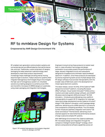
TECHNICAL BRIEFRF to mmWave Design for SystemsEmpowered by AWR Design Environment V16RF-enabled next-generation communication systems andconnected devices are differentiated by their performance,size, and cost. Traditionally, custom proprietary IC designs,leveraging the latest advanced-node technology, weredeveloped to meet these product requirements.Increasingly these challenges are being met by movingbeyond single IC solutions. Today’s electronic systems oftenintegrate heterogeneous technologies (Figure 1) to mitigatethe high cost of homogeneous system-on-chip (SoC)solutions by enabling designers to combine proven RFICand monolithic microwave IC (MMIC) designs on substratesusing newer packaging and integration technologies.Engineers trying to bring these products to market needbest-in-class simulation technology and designautomation to accurately predict the performance oflarger, densely integrated circuits and subsystemsdesigned for broadband and millimeter-wave (mmWave)spectrum. In addition, since these products are developedby diverse engineering teams across multiple design tools,RF design software must provide interoperability with thebroader class of EDA tools used in the development ofmixed-signal electronic systems.The latest release, version 16 (V16), of the Cadence AWRDesign Environment platform, including MicrowaveOffice software. Visual System Simulator (VSS) communications and radar systems design software, and AXIEM 3D planar electromagnetic (EM) and Analyst 3D FEMsimulators, introduces groundbreaking cross-platforminteroperability to support RF IP integration for heterogeneous technology development across Cadence Virtuoso ,Allegro PCB, Spectre simulation, and IC package designplatforms, delivering up to a 50% reduction in turnaroundtime compared to competing workflows. The V16 releasefurther introduces seamless integration with Clarity 3DSolver and Celsius Thermal Solver, delivering unconstrained capacity for electrothermal performance analysisof large-scale and complex RF systems.With AWR Design Environment V16, Cadence addressesRF/ microwave design and integration through thecompany’s Intelligent System Design strategy, whichdelivers computational software capabilities across allFigure 1. RF-enabled heterogeneous technologies integratedacross IC, package, and PCB
RF to mmWave Design for Systemsdesign elements of electronic systems. At the core of thisstrategy is design excellence, including an optimized EDAportfolio of tools with best-in-class RF, microwave, andmmWave circuit, system, and EM analysis, IP for semiconductor, package, and PCB design, and scalable access inthe cloud.Figure 2: Adaptive mesh of stacked MMIC die in package onPCB structureThe V16 AdvantageAdvanced integration methodologies result in smaller andmore efficient systems. However, these highly integratedsystems are more complicated and prone to error due tothe interdependencies of the individual components, thecomplex network of cross-fabric interconnects, and thechallenges of assembling cross-platform design data frommultiple sources. To address these design obstacles, AWRDesign Environment V16 provides an enhanced platform fordeveloping MMIC and RF PCB IP (Figure 2). Design teamscan incorporate their MMIC and RF PCB IP into electronicsystems composed of ICs and interposers, PCBs, andmodules from a wide array of process technologies throughproven capabilities in Cadence’s EDA software portfolio,including Allegro PCB Designer for PCBs and SiPs, and theVirtuoso platform for RFICs and modules.fPowerful - Turn concepts into real RF/microwavecomponents, optimized for performance and ready foreasy integration into multi-fabric systems that are rightthe first timefInsightful - Capture true RF system performance withtightly coupled EM and thermal analysis for solving large,complex structures and heat-generating RF powerapplicationsfConnected - Embeddable and re-usable MicrowaveOffice software ushers in a new era of unprecedentedcross-platform workflows to Allegro and Virtuosoplatforms for chip, package, board, and module designHighlightsPlatform InteroperabilityLeveraging shared architecture/data across Cadence EDAsolutions, the V16 release provides for new RF workflowsthat take completed IP design from Microwave Officesoftware and pass both the schematic and layout designsto the Virtuoso and/or Allegro platforms as data in a unifiedlibrary that contains all the building blocks of the circuitdesign. This enables design teams to operate the AllegroSiP or Virtuoso SiP bi-directional implementation flow andVirtuoso RF Solution physical implementation flow as theprimary layout tool, with the AWR Design Environmentsoftware providing the RF IP schematic/layout design data.The Virtuoso RF Solution flow captures Microwave Office RFIP, allowing designers to represent, integrate, and verify theMMIC and embedded RF package design within a singleenvironment. The shared database enables more practicalpackage and IC co-design by simplifying the design flowwith easy and reliable access to RF IP developed withinMicrowave Office software.Microwave Office/Virtuoso WorkflowExport IP generated from Microwave Office software andimplement it as MMIC or package/laminate technologies intoVirtuoso Schematic Editor and/or Virtuoso Layout Suite tointegrate these designs into multi-technology systems. Thenew interoperability eliminates the need for manual designre-entry, reducing time, costs, and the potential for errors.Schematic and layout sourced from Microwave Officesoftware will have the same look and feel in the Virtuosoenvironment as the original design (Figure 3). Since mostMMIC model and PCell libraries are defined and implementedby the III-V foundry as a process design kit (PDK), theMicrowave Office MMIC design flow still utilizes this PDK forthe target semiconductor process in the design.Microwave OfficeVirtuosoFigure 3. Microwave Office software’s 2-stage MMIC design(schematic/layout) integrated into the Virtuoso environmentwww.cadence.com2
RF to mmWave Design for SystemsThe Spectre Simulation Platform can simulate RF IP basedon Microwave Office software linear models, enablingco-design of RFICs, packages, and modules, inclusive of RFcontent such as off-chip matching and resonators. Forexample, Microwave Office software users can designpassive off-chip components through circuit design,optimization, and EM verification, and then decide the bestimplementation technology. In some cases, a network ofpassive components may be more optimally implementedacross the IC package boundary. This is often true for RFmodules, where the ideal filter design, matching networks,and power amplifier (PA) output stage load terminationoften leverage components on both the die and in thepackage substrate.Microwave Office/Allegro WorkflowRF/microwave IP created and analyzed in Microwave Officesoftware can be developed using Allegro libraries andtechnologies, ensuring compatibility with the Allegro PCBDesigner schematic and layout editors, as well as thetargeted manufacturing technologies using corporate-approved components. Using an organization’s approved billof materials (BOM) eliminates the need to replace components in the RF design when edited inside the manufacturing framework. In addition, physical design constraintsset in the Allegro platform are available within MicrowaveOffice software for dynamic voiding of ground/powerplanes.The Microwave Office to Allegro PCB workflow (Figure 4)provides a seamless schematic and layout data transferfrom Microwave Office software to Allegro PCB Designplatform, eliminating time-consuming and error-pronemanual re-entry. By using parts with identical symbols,footprints, and properties between Allegro and MicrowaveOffice software, RF designs are instantly recognizable to thelayout engineer, allowing RF and layout design teams towork collaboratively, yet independently. The Allegro designcan be imported back into the AWR Design Environmentplatform for high-performance, multiphysics analysis anddesign verification of the entire system after the RF IP hasbeen incorporated with the rest of the PCB.Microwave OfficeAXIEM, Analyst,Clarity, and CelsiusAllegroLayoutUnified LibrariesRF IPTechnology FileFigure 4. Design and manufacturing work flows forMicrowave Office/Allegro PCB support RF IP integration anddesign verificationMicrowave Office/High-PerformanceMultiphysics Analysis WorkflowClarity 3D Solver IntegrationLarge RF structures such as phased array feed networks areoften manually sectioned into smaller structures foranalysis using the largest and most powerful computingresources. The Clarity 3D Solver 3D EM simulator, used fordesigning critical interconnect, RFIC/MMIC, module, PCB,and SoIC designs, overcomes the limitations of legacy EManalysis software by leveraging Cadence’s distributedmultiprocessing technology to deliver virtually unlimitedcapacity and 10X speed.Figure 5. Clarity 3D Solver integration within the MicrowaveOffice software expands the available EM simulators to coverlarge, complex 3D structureswww.cadence.com3
RF to mmWave Design for SystemsNow integrated within AWR software, the Clarity 3D Solverprovides RF designers with ready access to high-capacityEM analysis for design verification and signoff of large,complex RF/ mixed-signal systems beyond the capabilitiesoffered by the AXIEM 3D planar and Analyst 3D finiteelement method (FEM) solvers.The Clarity 3D Solver integration with the Microwave Officesoftware (Figure 5) is an automated process in which theentire analysis experience is fully within the AWRenvironment. Once the simulation is complete, a datasetwith input geometry, simulation setup, and S-parameterresults is automatically assembled and associated with thegiven EM document for plot/measurement and subsequentextraction, circuit simulation, tuning, and optimization. Thelink also supports mesh, current, and field visualization datain addition to S-parameters, enabling designers to take fulladvantage of the rich set of EM 3D annotations that alreadyexist in the Microwave Office software.Celsius Thermal Solver IntegrationIC and electronic system companies, particularly thoseincorporating IC packaging and/or multi-technologymodules, face tremendous thermal challenges that cancause late-stage design modifications and derail projectschedules.The Celsius Thermal Solver embedded within the MicrowaveOffice software offers a solution (Figure 6) for RF PA andMMIC designs, RF PCBs, and modules, supporting electrothermal analysis through model information sourced fromMicrowave Office sofware’s project information, includingexisting MMIC (die or packaged device) design data andgeometries such as layout, material properties, and powersource values from RF simulation. Celsius Thermal Solverstructures can be created either by drawing/importing thegeometry in the EM editor, or using EM extraction withsimulated temperature results automatically returned intoMicrowave Office software.www.cadence.comFigure 6. The Celsius Thermal Solver’s analysis providescolor-coded temperature overlay on multi-cell GaN powerFET showing heat distribution across device3D plots of the thermal temperature distribution can beviewed in the Celsius Thermal Solver native editor. For MMICstructures, the solver also provides a full-chip temperatureprofile at the relevant resolution of the IC layout, available asa graphically viewable 3D structure temperature overlay inthe Celsius Thermal Solver’s native editor as well as atemperature-annotated netlist for circuit simulation.4
RF to mmWave Design for SystemsAdditional Analysis and Productivity EnhancementsEnvironment/AutomationCircuit Simulation Job scheduler now Robust parallel simplexsupports multiple simuloptimizers with variabletaneous remote queues,step size provide moreenabling designers to runflexibility and greaterlong circuit simulation orresistant to local minimaoptimization jobs in Microwave Office softparallel, either locally orware now supportsremotely, including Linuxmultiple versions of aclustersPDK within the same Version control manprojectages group design proj Support for new circuitects, allowing groupmodels and simulationdesign data managementmeasurementsof complex, multi-function designs and prevents unintentionaloverwriting when multiple users edit the samefile in central repository New Python supportoffers an alternateapproach for interfacingto the AWR DesignEnvironment platform bymeans of the pyawrlibrary, which incorporates win32com and addsAWR software-specificAPI functionalityEM SimulationSystem Simulation AXIEM: Store option Interconnect systemallows users to includeblock in VSS softwareor exclude the EM strucmodels the effects ofture’s de-embeddingtransmission line loss,network data in theimpedance mismatch,simulation data setand coupling AXIEM solver speed androbustness enhancements Analyst: Improvedsupport for multipleterminal configurationsin wave ports, includingstability and support formultiple positive terminals Analyst: Expandedfrequency modifiersettings for index inwhich the mesh will beadaptively refinedPhysical Design/Layout Dynamic voiding automatically adds clearancebetween layout shapesand nets as defined byconstraint rules Net management Enhanced VSS modelingfacilitates identificationof RF amplifiers inof net objects in layoutsaturation now yields aand schematicsmoother power output Connectivity modeversus power inputenables automaticcurveassociation of a shape to Frequency multiplieran overlapping netmodel for both saturated output power andspur level, yielding closeagreement betweentime domain, RF budgetanalysis, and RFI simulationsCadence is a pivotal leader in electronic design and computational expertise, using its IntelligentSystem Design strategy to turn design concepts into reality. Cadence customers are the world’smost creative and innovative companies, delivering extraordinary electronic products from chipsto boards to systems for the most dynamic market applications. www.cadence.com 2021 Cadence Design Systems, Inc. All rights reserved worldwide. Cadence, the Cadence logo, and the other Cadence marksfound at www.cadence.com/go/trademarks are trademarks or registered trademarks of Cadence Design Systems, Inc. All othertrademarks are the property of their respective owners.16708 06/21 SA/VY/PDF
developing MMIC and RF PCB IP (Figure 2). Design teams can incorporate their MMIC and RF PCB IP into electronic systems composed of ICs and interposers, PCBs, and modules from a wide array of process technologies through proven capabilities in Cadence's EDA software portfolio, including Allegro PCB Designer for PCBs and SiPs, and the