Transcription
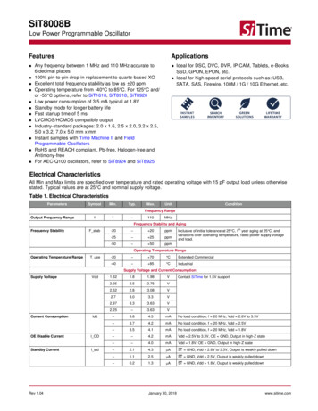
SiT8008BLow Power Programmable Oscillatorow Power, Standard Frequency OscillatorFeatures ApplicationsAny frequency between 1 MHz and 110 MHz accurate to6 decimal places100% pin-to-pin drop-in replacement to quartz-based XOExcellent total frequency stability as low as 20 ppmOperating temperature from -40 C to 85 C. For 125 C and/or -55 C options, refer to SiT1618, SiT8918, SiT8920Low power consumption of 3.5 mA typical at 1.8VStandby mode for longer battery lifeFast startup time of 5 msLVCMOS/HCMOS compatible outputIndustry-standard packages: 2.0 x 1.6, 2.5 x 2.0, 3.2 x 2.5,5.0 x 3.2, 7.0 x 5.0 mm x mmInstant samples with Time Machine II and FieldProgrammable OscillatorsRoHS and REACH compliant, Pb-free, Halogen-free andAntimony-freeFor AEC-Q100 oscillators, refer to SiT8924 and SiT8925 Ideal for DSC, DVC, DVR, IP CAM, Tablets, e-Books,SSD, GPON, EPON, etc.Ideal for high-speed serial protocols such as: USB,SATA, SAS, Firewire, 100M / 1G / 10G Ethernet, etc.Electrical CharacteristicsAll Min and Max limits are specified over temperature and rated operating voltage with 15 pF output load unless otherwisestated. Typical values are at 25 C and nominal supply voltage.Table 1. Electrical itConditionFrequency RangeOutput Frequency Range110MHzFrequency Stability and AgingFrequency StabilityF stab-20– 20ppm-25– 25ppm-50– 50ppmInclusive of initial tolerance at 25 C, 1st year aging at 25 C, andvariations over operating temperature, rated power supply voltageand load.Operating Temperature RangeOperating Temperature RangeT use-20– 70 CExtended Commercial-40– 85 CIndustrialSupply Voltage and Current ConsumptionSupply VoltageCurrent ConsumptionOE Disable CurrentStandby CurrentRev 1.04VddIddI ODI .973.33.63V2.25–3.63V–3.84.5mANo load condition, f 20 MHz, Vdd 2.8V to 3.3V–3.74.2mANo load condition, f 20 MHz, Vdd 2.5V–3.54.1mANo load condition, f 20 MHz, Vdd 1.8V––4.2mAVdd 2.5V to 3.3V, OE GND, Output in high-Z state––4.0mAVdd 1.8V, OE GND, Output in high-Z state–2.14.3 AST̅ ̅ ̅ GND, Vdd 2.8V to 3.3V, Output is weakly pulled down–1.12.5 AST̅ ̅ ̅ GND, Vdd 2.5V, Output is weakly pulled down–0.21.3 AST̅ ̅ ̅ GND, Vdd 1.8V, Output is weakly pulled downJanuary 30, 2018Contact SiTime for 1.5V supportwww.sitime.com
SiT8008B Low Power Programmable OscillatorTable 1. Electrical Characteristics onLVCMOS Output CharacteristicsDC45–55%All Vdds. See Duty Cycle definition in Figure 3 and Footnote 6Tr, Tf–12nsVdd 2.5V, 2.8V, 3.0V or 3.3V, 20% - 80%–1.32.5nsVdd 1.8V, 20% - 80%Vdd 2.25V - 3.63V, 20% - 80%Duty CycleRise/Fall Time––2nsOutput High VoltageVOH90%––VddOutput Low VoltageVOL––10%VddInput High VoltageVIH70%––VddPin 1, OE or ST̅ ̅̅Input Low VoltageVIL––30%VddPin 1, OE or ST̅ ̅̅Input Pull-up ImpedanceZ in5087150k Pin 1, OE logic high or logic low, or ST̅ ̅ ̅ logic high2––M Pin 1, ST̅ ̅ ̅ logic lowIOH -4 mA (Vdd 3.0V or 3.3V)IOH -3 mA (Vdd 2.8V and Vdd 2.5V)IOH -2 mA (Vdd 1.8V)IOL 4 mA (Vdd 3.0V or 3.3V)IOL 3 mA (Vdd 2.8V and Vdd 2.5V)IOL 2 mA (Vdd 1.8V)Input CharacteristicsStartup and Resume TimingStartup TimeT start––5msMeasured from the time Vdd reaches its rated minimum valueT oe––130nsf 110 MHz. For other frequencies, T oe 100 ns 3 * cyclesT resume––5msMeasured from the time ST̅ ̅ ̅ pin crosses 50% thresholdEnable/Disable TimeResume TimeJitterRMS Period JitterT jittPeak-to-peak Period JitterT pkRMS Phase Jitter (random)T phj–1.83psf 75 MHz, Vdd 2.5V, 2.8V, 3.0V or 3.3V–1.83psf 75 MHz, Vdd 1.8V–1225psf 75 MHz, Vdd 2.5V, 2.8V, 3.0V or 3.3V–1430psf 75 MHz, Vdd 1.8V–0.50.9psf 75 MHz, Integration bandwidth 900 kHz to 7.5 MHz–1.32psf 75 MHz, Integration bandwidth 12 kHz to 20 MHzTable 2. Pin DescriptionPinSymbolTop ViewFunctionality[1]Output Enable1OE/ST̅ ̅ ̅ /NCStandbyNo ConnectH : specified frequency outputL: output is high impedance. Only output driver is disabled.OE/ST/NCH[1]: specified frequency outputL: output is low (weak pull down). Device goes to sleep mode. Supplycurrent reduces to I std.Any voltage between 0 and Vdd or Open[1]: Specified frequencyoutput. Pin 1 has no function.2GNDPowerElectrical ground3OUTOutputOscillator output4VDDPowerPower supply voltage[2]Figure 1. Pin AssignmentsNotes:1. In OE or ST̅ ̅ ̅ mode, a pull-up resistor of 10 kΩ or less is recommended if pin 1 is not externally driven. If pin 1 needs to be left floating, use the NC option.2. A capacitor of value 0.1 µF or higher between Vdd and GND is required.Rev 1.04Page 2 of 17www.sitime.com
SiT8008B Low Power Programmable OscillatorTable 3. Absolute Maximum LimitsAttempted operation outside the absolute maximum ratings may cause permanent damage to the part. Actual performanceof the IC is only guaranteed within the operational specifications, not at absolute maximum ratings.ParameterMin.Max.UnitStorage Temperature-65150 CVdd-0.54VElectrostatic Discharge–2000VSoldering Temperature(follow standard Pb free soldering guidelines)–260 C[3]–150 CJunction TemperatureNote:3. Exceeding this temperature for extended period of time may damage the device.Table 4. Thermal Consideration[4]Package JA, 4 Layer Board JA, 2 Layer Board JC, Bottom( C/W)( C/W)( 6201615225236Note:4. Refer to JESD51 for JA and JC definitions, and reference layout used to determine the JA and JC values in the above table.Table 5. Maximum Operating Junction Temperature[5]Max Operating Temperature (ambient)Maximum Operating Junction Temperature70 C80 C85 C95 CNote:5. Datasheet specifications are not guaranteed if junction temperature exceeds the maximum operating junction temperature.Table 6. Environmental ComplianceParameterCondition/Test MethodMechanical ShockMIL-STD-883F, Method 2002Mechanical VibrationMIL-STD-883F, Method 2007Temperature CycleJESD22, Method A104SolderabilityMIL-STD-883F, Method 2003Moisture Sensitivity LevelMSL1 @ 260 CRev 1.04Page 3 of 17www.sitime.com
SiT8008B Low Power Programmable OscillatorTest Circuit and Waveform[6]VddVoutTest PointtrPowerSupply4312tf80% Vdd15pF(including probeand fixturecapacitance)0.1 uF50%20% VddHigh Pulse(TH)Low Pulse(TL)VddPeriod1 kΩOE/ST FunctionFigure 3. WaveformFigure 2. Test CircuitNote:6. Duty Cycle is computed as Duty Cycle TH/Period.Timing Diagrams90% VddVddVdd50% VddPin 4 VoltageT start[7]No Glitchduring start upT resumeST VoltageCLK OutputCLK OutputHZHZT start: Time to start from power-offT resume: Time to resume from STFigure 4. Startup Timing (OE/ ST̅ ̅ ̅ Mode)Figure 5. Standby Resume Timing ( ST̅ ̅ ̅ Mode Only)VddVdd50% VddOE VoltageOE VoltageT oe50% VddT oeCLK OutputCLK OutputHZHZT oe: Time to re-enable the clock outputT oe: Time to put the output in High Z modeFigure 6. OE Enable Timing (OE Mode Only)Figure 7. OE Disable Timing (OE Mode Only)Note:7. SiT8008 has “no runt” pulses and “no glitch” output during startup or resume.Rev 1.04Page 4 of 17www.sitime.com
SiT8008B Low Power Programmable OscillatorPerformance DUT8DUT9DUT102015Frequency (ppm)5.55.0Idd 8090100-40110-30-20-10Frequency (MHz)Figure 8. Idd vs Frequency1.8 V2.5 V2.8 V3.0 V01020304050607080Temperature ( C)Figure 9. Frequency vs Temperature3.3 V1.8 V2.5 V2.8 V3.0 V3.3 V55RMS period jitter (ps)5453ty cyc(52515049484746450Frequency (MHz)2030405060708090100110Frequency (MHz)Figure 10. RMS Period Jitter vs FrequencyFigure 11. Duty Cycle vs FrequencyTemperature ( C)Temperature ( C)Figure 12. 20%-80% Rise Time vs TemperatureRev 1.0410Page 5 of 17Figure 13. 20%-80% Fall Time vs Temperaturewww.sitime.com
SiT8008B Low Power Programmable OscillatorPerformance Plots[8]1.8 V2.5 V2.8 V3.0 V3.3 V0.9IPJ ency (MHz)Frequency (MHz)Figure 15. RMS Integrated Phase Jitter Random(900 kHz to 20 MHz) vs Frequency[9]Figure 14. RMS Integrated Phase Jitter Random(12 kHz to 20 MHz) vs Frequency[9]Notes:8. All plots are measured with 15 pF load at room temperature, unless otherwise stated.9. Phase noise plots are measured with Agilent E5052B signal source analyzer. Integration range is up to 5 MHz for carrier frequencies below 40 MHz.Rev 1.04Page 6 of 17www.sitime.com
SiT8008B Low Power Programmable OscillatorProgrammable Drive StrengthThe SiT8008 includes a programmable drive strengthfeature to provide a simple, flexible tool to optimize theclock rise/fall time for specific applications. Benefits fromthe programmable drive strength feature are: Improves system radiated electromagnetic interference(EMI) by slowing down the clock rise/fall time. Improves the downstream clock receiver’s (RX) jitter bydecreasing (speeding up) the clock rise/fall time.The SiT8008 can support up to 60 pF or higher inmaximum capacitive loads with drive strength settings.Refer to the Rise/Fall Time Tables (Table 7 to 11) todetermine the proper drive strength for the desiredcombination of output load vs. rise/fall time.SiT8008 Drive Strength SelectionTables 7 through 11 define the rise/fall time for a givencapacitive load and supply voltage.1.Ability to drive large capacitive loads while maintainingfull swing with sharp edge rates.Select the table that matches the SiT8008 nominalsupply voltage (1.8V, 2.5V, 2.8V, 3.0V, 3.3V).2.For more detailed information about rise/fall time controland drive strength selection, see the SiTime ApplicationNotes section.Select the capacitive load column that matchesthe application requirement (5 pF to 60 pF)3.Under the capacitive load column, select thedesired rise/fall times.4.The left-most column represents the part numbercode for the corresponding drive strength.5.Add the drive strength code to the part number forordering purposes. EMI Reduction by Slowing Rise/Fall TimeFigure 16 shows the harmonic power reduction as therise/fall times are increased (slowed down). The rise/falltimes are expressed as a ratio of the clock period. For theratio of 0.05, the signal is very close to a square wave. Forthe ratio of 0.45, the rise/fall times are very close to neartriangular waveform. These results, for example, show thatthe 11th clock harmonic can be reduced by 35 dB if therise/fall edge is increased from 5% of the period to 45% ofthe period.trise 0.05trise 0.1trise 0.15trise 0.2trise 0.25trise 0.3trise 0.35trise 0.4trise 0.4510Harmonic amplitude (dB)0-10-20Calculating Maximum FrequencyAny given rise/fall time in Table 7 through 11 dictates themaximum frequency under which the oscillator can operatewith guaranteed full output swing over the entire operatingtemperature range. This max frequency can be calculatedas the following:Max Frequency 15 x Trf 20/80where Trf 20/80 is the typical value for 20%-80% rise/fall time.-30-40Example 1-50-60Calculate fMAX for the following condition:-70-8013579 Vdd 1.8V (Table 7) Capacitive Load: 30 pF Desired Tr/f time 3 ns(rise/fall time part number code E) fMAX 66.66666011Harmonic numberFigure 16. Harmonic EMI reduction as a Functionof Slower Rise/Fall TimeJitter Reduction with Faster Rise/Fall TimePower supply noise can be a source of jitter for the downstream chipset. One way to reduce this jitter is to speed upthe rise/fall time of the input clock. Some chipsets may alsorequire faster rise/fall time in order to reduce their sensitivityto this type of jitter. Refer to the Rise/Fall Time Tables(Table 7 to Table 11) to determine the proper drive strength.High Output Load CapabilityPart number for the above example:SiT8008IE12-18E-66.666660Drive strength code is inserted here. Default setting is “-”The rise/fall time of the input clock varies as a function ofthe actual capacitive load the clock drives. At any givendrive strength, the rise/fall time becomes slower as theoutput load increases. As an example, for a 3.3V SiT8008device with default drive strength setting, the typical rise/falltime is 1 ns for 15 pF output load. The typical rise/fall timeslows down to 2.6 ns when the output load increases to 45 pF.One can choose to speed up the rise/fall time to 1.83 ns bythen increasing the drive strength setting on the SiT8008.Rev 1.04Page 7 of 17www.sitime.com
SiT8008B Low Power Programmable OscillatorRise/Fall Time (20% to 80%) vs CLOAD TablesTable 8. Vdd 2.5V Rise/Fall Timesfor Specific CLOADTable 7. Vdd 1.8V Rise/Fall Timesfor Specific CLOADRise/Fall Time Typ (ns)Rise/Fall Time Typ (ns)Drive Strength \ CLOAD5 pF15 pF30 pF45 pF60 pFDrive Strength \ CLOAD5 pF15 pF30 pF45 pF60 pFLARBTEUF or "‐": 214.4711.086.485.745.094.56LARBTE or "‐": 3.102.792.544.013.653.3245 pF18.749.866.765.203.072.712.402.1660 pF24.3012.688.626.643.903.513.132.85Table 9. Vdd 2.8V Rise/Fall Timesfor Specific CLOADTable 10. Vdd 3.0V Rise/Fall Timesfor Specific CLOADRise/Fall Time Typ (ns)Rise/Fall Time Typ (ns)Drive Strength \ CLOADLARBT5 pF3.771.941.290.970.5515 pF7.543.902.572.001.1230 pF12.287.034.723.542.0845 pF19.5710.247.015.433.2260 pF25.2713.349.066.934.08E or "‐": .522.293.673.302.99Drive Strength \ CLOADLARBT or "‐": defaultEUF5 pF3.601.841.220.890.510.380.300.2715 pF7.213.712.461.921.000.920.830.7630 pF11.976.724.543.391.971.721.551.39Table 11. Vdd 3.3V Rise/Fall Timesfor Specific CLOADRise/Fall Time Typ (ns)Drive Strength \ CLOAD5 pF15 pF30 pF45 pF60 93.2217.568.986.044.5223.5912.198.346.33T or "‐": 1.461.312.602.302.051.833.843.352.932.61Rev 1.04Page 8 of 17www.sitime.com
SiT8008B Low Power Programmable OscillatorPin 1 Configuration Options (OE, ST̅ ̅ ̅ , or NC)Pin 1 of the SiT8008 can be factory-programmed to supportthree modes: Output Enable (OE), Standby (ST̅ ̅ ̅ ) orNo Connect (NC). These modes can also be programmedwith the Time Machine using field programmable devices.Output Enable (OE) ModeIn the OE mode, applying logic Low to the OE pin onlydisables the output driver and puts it in Hi-Z mode. Thecore of the device continues to operate normally. Powerconsumption is reduced due to the inactivity of the output.When the OE pin is pulled High, the output is typicallyenabled in 1 µs.Standby (ST̅ ̅ ̅ ) ModeIn the ST̅ ̅ ̅ mode, a device enters into the standby modewhen Pin 1 pulled Low. All internal circuits of the device areturned off. The current is reduced to a standby current,typically in the range of a few µA. When ST̅ ̅ ̅ is pulled High,the device goes through the “resume” process, which cantake up to 5 ms.No Connect (NC) ModeIn the NC mode, the device always operates in its normalmode and outputs the specified frequency regardless of thelogic level on pin 1.Figure 18. Startup Waveform vs. Vdd(Zoomed-in View of Figure 17)Instant Samples with Time Machine andField Programmable OscillatorsSiTime supports a field programmable version of the SiT8008low power oscillator for fast prototyping and real timecustomization of features. The field programmable devices(FP devices) are available for all five standard SiT8008package sizes and can be configured to one’s exactspecification using the Time Machine II, an USB poweredMEMS oscillator programmer.Customizable Features of the SiT8008 FP Devices IncludeTable 12 below summarizes the key relevant parametersin the operation of the device in OE, ST̅ ̅ ̅ , or NC mode.Table 12. OE vs. ST̅ ̅ ̅ vs. NCOEActive current 20 MHz (max, 1.8V)OE disable current (max. 1.8V)Standby current (typical 1.8V)OE enable time at 77.76 MHz (max)Resume time from standby(max, all frequency)Output driver in OE disable/standbymode4.1 mA4 mAN/AST̅ ̅̅4.1 mA Frequency between 1 MHz to 110 MHz Three frequency stability options, 20 ppm, 25 ppm, 50 ppm Two operating temperatures, -20 to 70 C or-40 to 85 C Six supply voltage options, 1.8V, 2.5V, 2.8V, 3.0V,3.3V and 2.25 to 3.63V continuous Output drive strength OE, ST̅ ̅ ̅ or NC modeNC4.1 mAN/AN/A0.6 µAN/A138 nsN/AN/AN/A5 msN/AHigh Zweakpull-downN/AOutput on Startup and ResumeThe SiT8008 comes with gated output. Its clock output isaccurate to the rated frequency stability within the first pulsefrom initial device startup or resume from the standby mode.For more information regarding SiTime’s field programmablesolutions, see Time Machine II and Field ProgrammableOscillators.SiT8008 is typically factory-programmed per customerordering codes for volume delivery.In addition, the SiT8008 features “no runt” pulses and “noglitch” output during startup or resume as shown in thewaveform captures in Figure 17 and Figure 18.Figure 17. Startup Waveform vs. VddRev 1.04Page 9 of 17www.sitime.com
SiT8008B Low Power Programmable OscillatorDimensions and PatternsPackage Size – Dimensions (Unit: mm)[10]Recommended Land Pattern (Unit: mm)[11]2.0 x 1.6 x 0.75 mm2.5 x 2.0 x 0.75 mm2.5 0.05#41.51.1#30.5#2#2#11.0YXXXX#11.91.00#32.0 0.05#40.751.10.75 0.053.2 x 2.5 x 0.75 mm3.2 0.052.22.1#3#4#11.90.7YXXXX#2#21.2#32.5 0.050.9#4#10.91.40.75 0.055.0 x 3.2 x 0.75 mm2.545.0 0.05#2#12.2#21.6#1#41.1YXXXX#30.8#33.2 0.05#42.391.151.50.75 0.05Rev 1.04Page 10 of 17www.sitime.com
SiT8008B Low Power Programmable OscillatorDimensions and PatternsPackage Size – Dimensions (Unit: mm)[10]Recommended Land Pattern (Unit: mm)[11]7.0 x 5.0 x 0.90 mm5.083.812.65.082.01.1YXXXX5.0 0.057.0 0.051.42.20.90 0.10Notes:10. Top marking: Y denotes manufacturing origin and XXXX denotes manufacturing lot number. The value of “Y” will depend on the as sembly location ofthe device.11. A capacitor of value 0.1 µF or higher between Vdd and GND is required.Rev 1.04Page 11 of 17www.sitime.com
SiT8008B Low Power Programmable OscillatorOrdering InformationThe Part No. Guide is for reference only. To customize and build an exact part number, use the SiTimePart Number Generator.SiT8008BC-12-18E- 66.666660DPacking MethodRevision LetterTemperature Rangeal, -20ºC toSupply VoltagePackage SizeFrequency StabilityTable 13. Ordering Codes for Supported Tape & Reel Packing MethodDevice Size(mm x mm)16 mm T&R (3ku)16 mm T&R (1ku)12 mm T&R (3ku)12 mm T&R (1ku)8 mm T&R (3ku)8 mm T&R (1ku)2.0 x 1.6––––DE2.5 x 2.0––––DE3.2 x 2.5––––DE5.0 x 3.2––TY––7.0 x 5.0TY––––Rev 1.04Page 12 of 17www.sitime.com
SiT8008B Low Power Programmable OscillatorTable 14. Additional InformationDocumentDescriptionDownload LinkTime Machine IIMEMS oscillator ne-oscillator-programmerField ProgrammableOscillatorsDevices that can be programmable in the field byTime Machine e-oscillatorsManufacturing NotesTape & Reel dimension, reflow profile and othermanufacturing related fication ReportsRoHS report, reliability reports, composition eliabilityPerformance ReportsAdditional performance data such as phase noise,current consumption and jitter for selected ce-measurement-reportTermination TechniquesTermination design cation-notesLayout TechniquesLayout cation-notesTable 15. Revision HistoryRevisionRelease Date1.006/10/2014First Production ReleaseChange Summary1.0105/07/20151.0206/18/2015Revised the Electrical Characteristics, Timing Diagrams and Performance PlotsRevised 2016 package diagramAdded 16 mm T&R information to Table 13Revised 12 mm T&R information to Table 131.0308/30/2016Revised part number example in the ordering information1.0401/30/2018Updated logo and company address, other page layout changesRevised 2520 package land patternSiTime Corporation, 5451 Patrick Henry Drive, Santa Clara, CA 95054, USA Phone: 1-408-328-4400 Fax: 1-408-328-4439 SiTime Corporation 2014-2018. The information contained herein is subject to change at any time without notice. SiTime assumes no responsibility or liability f or any loss, damageor defect of a Product which is caused in whole or in part by (i) use of any circuitry other than circuitry embodied in a SiTime product, (ii) misuse or abuse including static discharge, neglector accident, (iii) unauthorized modification or repairs which have been soldered or altered during assembly and are not capable of being tested by SiTime under its normal test conditions, or(iv) improper installation, storage, handling, warehousing or transportation, or (v) being subjected to unusual physical, thermal, or electrical stress.Disclaimer: SiTime makes no warranty of any kind, express or implied, with regard to this material, and specifically disclaims any and all express or implied warranties, either in fact or byoperation of law, statutory or otherwise, including the implied warranties of merchantability and fitness for use or a particular purpose, and any implied warranty arising from course of dealing orusage of trade, as well as any common-law duties relating to accuracy or lack of negligence, with respect to this material, any SiTime product and any product documentation. Products sold bySiTime are not suitable or intended to be used in a life support application or component, to operate nuclear facilities, or in other mission critical applications where human life may be involvedor at stake. All sales are made conditioned upon compliance with the critical uses policy set forth below.CRITICAL USE EXCLUSION POLICYBUYER AGREES NOT TO USE SITIME'S PRODUCTS FOR ANY APPLICATION OR IN ANY COMPONENTS USED IN LIFE SUPPORT DEVICES OR TO OPERATE NUCLEARFACILITIES OR FOR USE IN OTHER MISSION-CRITICAL APPLICATIONS OR COMPONENTS WHERE HUMAN LIFE OR PROPERTY MAY BE AT STAKE.SiTime owns all rights, title and interest to the intellectual property related to SiTime's products, including any software, firmware, copyright, patent, or trademark. The sale of SiTime products doesnot convey or imply any license under patent or other rights. SiTime retains the copyright and trademark rights in all documents, catalogs and plans supplied pursuant to or ancillary to the saleof products or services by SiTime. Unless otherwise agreed to in writing by SiTime, any reproduction, modification, translation, compilation, or representation of this material shall be strictlyprohibited.Rev 1.04Page 13 of 17www.sitime.com
Silicon MEMS Outperforms QuartzSupplemental InformationThe Supplemental Information section is not part of the datasheet and is for informational purposes only.Rev 1.04Page 14 of 17www.sitime.com
Silicon MEMS Outperforms QuartzBest ReliabilityBest Electro Magnetic Susceptibility (EMS)Silicon is inherently more reliable than quartz. Unlikequartz suppliers, SiTime has in-house MEMS and analogCMOS expertise, which allows SiTime to develop themost reliable products. Figure 1 shows a comparisonwith quartz technology.SiTime’s oscillators in plastic packages are up to 54 timesmore immune to external electromagnetic fields thanquartz oscillators as shown in Figure 3.Why is SiTime Best in Class:Why is SiTime Best in Class:SiTime’s MEMS resonators are vacuum sealedusing an advanced EpiSeal process, whicheliminates foreign particles and improves longterm aging and reliability Internal differential architecture for best commonmode noise rejection Electrostatically driven MEMS resonator is moreimmune to EMSWorld-class MEMS and CMOS design expertise Reliability (Million 8Figure 3. Electro Magnetic Susceptibility (EMS)Figure 1. Reliability ComparisonBest Power Supply Noise Rejection[1]SiTime’s MEMS oscillators are more resilient against noiseon the power supply. A comparison is shown in Figure 4.Best AgingUnlike quartz, MEMS oscillators have excellent longterm aging performance which is why every new SiTimeproduct specifies 10-year aging. A comparison is shownin Figure 2.Why is SiTime Best in Class:Why is SiTime Best in Class:SiTime’s MEMS resonators are vacuum sealedusing an advanced EpiSeal process, whicheliminates foreign particles and improves longterm aging and reliability [3] On-chip regulators and internal differentialarchitecture for common mode noise rejection MEMS resonator is paired with advanced analogCMOS ICSiTimeEPSNKYCAInherently better immunity of electrostaticallydriven MEMS resonator MEMS vs. Quartz artzOscillatorOscillator108Aging ( PPM)864233.5Figure 4. Power Supply Noise Rejection[4]1.501-Year10-Year[2]Figure 2. Aging ComparisonRev 1.04Page 15 of 17www.sitime.com
Silicon MEMS Outperforms QuartzBest Vibration RobustnessBest Shock RobustnessHigh-vibration environments are all around us. All electronics,from handheld devices to enterprise servers and storagesystems are subject to vibration. Figure 5 shows acomparison of vibration robustness.SiTime’s oscillators can withstand at least 50,000 g shock.They all maintain their electrical performance in operationduring shock events. A comparison with quartz devices isshown in Figure 6.Why is SiTime Best in Class:Why is SiTime Best in Class: The moving mass of SiTime’s MEMS resonatorsis up to 3000 times smaller than quartz The moving mass of SiTime’s MEMS resonatorsis up to 3000 times smaller than quartz Center-anchored MEMS resonator is the mostrobust design Center-anchored MEMS resonator is the mostrobust designVibration Sensitivity (ppb/g)TXCTXCEPSCWKYCAKYCASLABEpiSealSiTime MEMS100.010.01.00.10.0101001000KYCAVibration Frequency (Hz)Figure 5. Vibration Robustness[5]EPSNTXCCWSLABSiTime[6]Figure 6. Shock RobustnessFigure labels: TXC TXCEpson EPSNConnor Winfield CWKyocera KYCASiLabs SLABSiTime EpiSeal MEMSRev 1.04Page 16 of 17www.sitime.com
Silicon MEMS Outperforms QuartzNotes:1. Data source: Reliability documents of named companies.2. Data source: SiTime and quartz oscillator devices datasheets.3. Test conditions for Electro Magnetic Susceptibility (EMS): According to IEC EN61000-4.3 (Electromagnetic compatibility standard) Field strength: 3V/m Radiated signal modulation: AM 1 kHz at 80% depth Carrier frequency scan: 80 MHz – 1 GHz in 1% steps Antenna polarization: Vertical DUT position: Center aligned to antennaDevices used in this test:LabelManufacturerPart NumberTechnologyEpiSeal MEMSSiTimeSiT9120AC-1D2-33E156.250000MEMS PLLEPSNEpsonEG-2102CA156.2500M-PHPAL3Quartz, SAWTXCTXCBB-156.250MBE-TQuartz, 3 OvertoneCWConner WinfieldP123-156.25MQuartz, 3rd OvertoneKYCAAVX KyoceraKC7050T156.250P30E00Quartz, SAWSLABSiLab590AB-BDGQuartz, 3rd Overtone PLLLabelManufacturerPart NumberTechnologyEpiSeal MEMSSiTimeSiT8208AI-33-33E-25.000000MEMS PLLNDKNDKNZ2523SB-25.6MQuartzKYCAAVX 5M0-MB3Quartzrd4. 50 mV pk-pk Sinusoidal voltage.Devices used in this test:5. Devices used in this test:same as EMS test stated in Note 3.6. Test conditions for shock test: MIL-STD-883F Method 2002 Condition A: half sine wave shock pulse, 500-g, 1ms Continuous frequency measurement in 100 μs gate time for 10 secondsDevices used in this test:same as EMS test stated in Note 3.7. Additional data, including setup and detailed results, is available upon request to qualified customer. Please contact productsupport@sitime.com.Rev 1.04Page 17 of 17www.sitime.com
SiT8008B Low Power Programmable Oscillator ow Power, Standard Frequency Oscillator Features Any frequency between 1 MHz and 110 MHz accurate to 6 decimal places 100% pin-to-pin drop-in replacement to quartz-based XO Excellent total frequency stability as low as 20 ppm Operating temperature from -40 C to 85 C. For 125 C and/ or -55 C options, refer to SiT1618, SiT8918, SiT8920