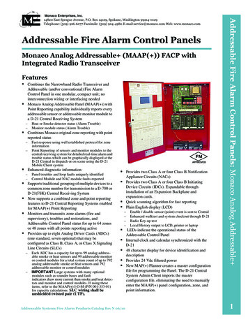
Transcription
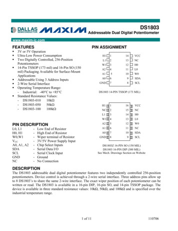
DS1803Addressable Dual Digital Potentiometerwww.maxim-ic.comFEATURES PIN ASSIGNMENT3V or 5V OperationUltra-Low Power ConsumptionTwo Digitally Controlled, 256-PositionPotentiometers14-Pin TSSOP (173 mil) and 16-Pin SO (150mil) Packaging Available for Surface-MountApplicationsAddressable Using 3 Address Inputs2-Wire Serial InterfaceOperating Temperature Range:- Industrial: -40 C to 85 CStandard Resistance Values:- DS1803-01010kΩ- DS1803-05050kΩ- 0A069SDAGND78SCLDS1803 14-PIN TSSOP (173 MIL)PIN DESCRIPTIONL0, L1H0, H1W0,W1VCCA0, A1, A2SDASCLGNDNCH1Low End of ResistorHigh End of ResistorWiper terminal of Resistor3V/5V Power Supply InputChip Select InputsSerial Data I/OSerial Clock InputGroundNo 1NCA0710SDAGND89SCLDS1803Z 16-PIN SO (150 MIL)DS1803 16-PIN DIP (300 MIL)See Mech. Drawings Section on WebsiteDESCRIPTIONThe DS1803 addressable dual digital potentiometer features two independently controlled 256-positionpotentiometers. Device control is achieved through a 2-wire serial interface. Three address pins allow upto 8 DS1803’s to share the same 2-wire interface. The exact wiper position of each potentiometer can bewritten or read. The DS1803 is available in a 16-pin DIP, 16-pin SO, and 14-pin TSSOP package. Thedevice is available in three standard resistance values: 10kΩ, 50kΩ, and 100kΩ and is specified over theindustrial temperature range.1 of 11110706
DS1803DEVICE OPERATIONThe DS1803 is an addressable, digitally controlled device which has two 256-position potentiometers. Afunctional block diagram of the part is shown in Figure 1. Communication and control of the device isaccomplished via a 2-wire serial interface. Address inputs A0, A1, and A2 allow up to 8 DS1803s toshare the same 2-wire interface.Each potentiometer is composed of a 256 position resistor array. Two 8-bit registers, each assigned to arespective potentiometer, are used to set the wiper position on the resistor array. The wiper terminal ismultiplexed to one of 256 positions on the resistor array based on its corresponding 8-bit register value.For example, the high-end terminals, H0 and H1, have wiper position values FFh while the low-endterminals, L0 and L1, have wiper position values 00h.The DS1803 is a volatile device that does not maintain the position of the wiper during power-down orloss of power. On power-up, the DS1803 wipers’ position will be set to position 00h - the low-endterminals. The user may then set the wiper value to a desired position.Communication with the DS1803 takes place over the 2-wire serial interface consisting of the bidirectional pin, SDA, and the serial clock input, SCL. Complete details of the 2-wire interface arediscussed in the section entitled “2-wire Serial Data Bus.”Application ConsiderationsThe DS1803 is offered in three standard resistor values, which include 10kΩ, 50kΩ, and 100kΩ. Theresolution of the potentiometer is defined as RTOT/255, where RTOT is the total resistor value of thepotentiometer. The DS1803 is designed to operate using 3V or 5V power supplies over the industrial(-40 C to 85 C) temperature range. Maximum input signal levels across the potentiometer cannotexceed the operating power supply of the device.2-WIRE SERIAL DATA BUSThe DS1803 supports a bi-directional 2-wire bus and data transmission protocol. A device that sends dataon the bus is defined as a transmitter, and a device receiving data as a receiver. The device that controlsthe message is called a “master”. The devices that are controlled by the master are “slaves”. The bus mustbe controlled by a master device which generates the serial clock (SCL), controls the bus access, andgenerates the START and STOP conditions. The DS1803 operates as a slave on the 2-wire bus.Connections to the bus are made via the open-drain I/O lines SDA and SCL.The following bus protocol has been defined (see Figure 2). Data transfer may be initiated only when the bus is not busy. During data transfer, the data line must remain stable whenever the clock line is HIGH. Changes inthe data line while the clock line is high will be interpreted as control signals.Accordingly, the following bus conditions have been defined:Bus not busy: Both data and clock lines remain HIGH.Start data transfer: A change in the state of the data line, from HIGH to LOW, while the clock isHIGH, defines a START condition.2 of 11
DS1803Stop data transfer: A change in the state of the data line, from LOW to HIGH, while the clock line isHIGH, defines the STOP condition.Data valid: The state of the data line represents valid data when, after a START condition, the data lineis stable for the duration of the HIGH period of the clock signal. The data on the line must be changedduring the LOW period of the clock signal. There is one clock pulse per bit of data. Figure 2 details howdata transfer is accomplished on the 2-wire bus. Depending upon the state of the R/ W * bit, two types ofdata transfer are possible.Each data transfer is initiated with a START condition and terminated with a STOP condition. Thenumber of data bytes transferred between START and STOP conditions is not limited, and is determinedby the master device. The information is transferred byte-wise and each receiver acknowledges with aninth bit.Acknowledge: Each receiving device, when addressed, is obliged to generate an acknowledge after thereception of each byte. The master device must generate an extra clock pulse which is associated with thisacknowledge bit.A device that acknowledges must pull down the SDA line during the acknowledge clock pulse in such away that the SDA line is stable LOW during the HIGH period of the acknowledge related clock pulse. Ofcourse, setup and hold times must be taken into account. A master must signal an end of data to the slaveby not generating an acknowledge bit on the last byte that has been clocked out of the slave. In this case,the slave must leave the data line HIGH to enable the master to generate the STOP condition.1. Data transfer from a master transmitter to a slave receiver: The first byte transmitted by themaster is the control byte (slave address). Next follows a number of data bytes. The slave returns anacknowledge bit after each received byte.2. Data transfer from a slave transmitter to a master receiver: The first byte (the slave address) istransmitted by the master. The slave then returns an acknowledge bit. Next follows a number of databytes transmitted by the slave to the master. The master returns an acknowledge bit after all receivedbytes other than the last byte. At the end of the last received byte, a ‘not acknowledge’ is returned.The master device generates all of the serial clock pulses and the START and STOP conditions. Atransfer is ended with a STOP condition or with a repeated START condition. Since a repeated STARTcondition is also the beginning of the next serial transfer, the bus will not be released.The DS1803 may operate in the following two modes:1. Slave receiver mode: Serial data and clock are received through SDA and SCL. After each byte isreceived, an acknowledge bit is transmitted. START and STOP conditions are recognized as thebeginning and end of a serial transfer. Address recognition is performed by hardware after receptionof the slave address and direction bit.2. Slave transmitter mode: The first byte is received and handled as in the slave receiver mode.However, in this mode the direction bit will indicate that the transfer direction is reversed. Serial datais transmitted on SDA by the DS1803 while the serial clock is input on SCL. START and STOPconditions are recognized as the beginning and end of a serial transfer.3 of 11
DS1803SLAVE ADDRESSThe control byte is the first byte received following the START condition from the master device. Thecontrol byte consists of a four bit control code; for the DS1803, this is 0101 binary. The next three bits ofthe control byte are the device select bits (A2, A1, A0). They are used by the master device to selectwhich of the devices on the bus are to be accessed. The last bit of the control byte (R/ W *) defines theoperation to be performed. When set to a one a read operation is selected, and when set to a zero a writeoperation is selected. Figure 3 shows the control byte for the DS1803.Following the START condition, the DS1803 monitors the SDA bus for the control byte beingtransmitted. Upon receiving a matching control byte, the DS1803 outputs an acknowledge signal on theSDA line.COMMAND AND PROTOCOLThe command and protocol structure of the DS1803 allows the user to read or write the potentiometer(s).The command structures for the part are presented in Figures 4 and 5. Data is transmitted most significantbit (MSB) first. During communication, the receiving unit always generates the acknowledge.Reading the DS1803As shown in Figure 4, the DS1803 provides one read command operation. This operation allows the userto read both potentiometers. Specifically, the R/ W bit of the control byte is set equal to a 1 for a readoperation. Communication to read the DS1803 begins with a START condition which is issued by themaster device. The control byte from the master device will follow the START condition. Once thecontrol byte has been received by the DS1803, the part will respond with an ACKNOWLEDGE. TheR/ W bit of the control byte as stated should be set equal to ‘1’ for reading the DS1803.When the master has received the ACKNOWLEDGE from the DS1803, the master can then begin toreceive potentiometer wiper data. The value of the potentiometer-0 wiper position will be the firstreturned from the DS1803. Once the eight bits of the potentiometer-0 wiper position has been transmitted,the master will need to issue an ACKNOWLEDGE, unless it is the only byte to be read, in which case themaster issues a NOT ACKNOWLEDGE. If desired the master may stop the communication transfer atthis point by issuing the STOP condition. However, if the value of the potentiometer-1 wiper positionvalue is needed, communication transfer can continue by clocking the remaining eight bits of thepotentiometer-1 value, followed by an NOT ACKNOWLEDGE. Final communication transfer isterminated by issuing the STOP command.Writing the DS1803A data flow diagram for writing the DS1803 is shown in Figure 5. The DS1803 has three writecommands. These include write pot-0, write pot-1, and write pot-0/1. The write pot-0 command allowsthe user to write the value of potentiometer-0 and as an option the value of potentiometer-1. The write-1command allows the user to write the value of potentiometer-1 only. The last write command, write-0/1,allows the user to write both potentiometers to the same value with one command and one data valuebeing issued.All the write operations begin with a START condition. Following the START condition, the masterdevice will issue the control byte. The read/write bit of the control byte will be set to ‘0’ for writing theDS1803. Once the control byte has been issued and the master receives the acknowledgment from theDS1803, the command byte is transmitted to the DS1803. As mentioned above, there exist three write4 of 11
DS1803operations that can be used with the DS1803. The binary value of each write command is shown in Figure5 and also in the Table 1.2-WIRE COMMAND WORDS Table 1COMMANDCOMMAND VALUEWrite Potentiometer-0101010 01Write Potentiometer-1101010 10Write Both Potentiometers101011 115 of 11
DS1803ABSOLUTE MAXIMUM RATINGS*Voltage on Any Pin Relative to GroundOperating TemperatureStorage TemperatureSoldering Temperature-1.0V to 7.0V-40 to 85 C; industrial-55 C to 125 C260 C for 10 seconds* This is a stress rating only and functional operation of the device at these or any other conditions abovethose indicated in the operation sections of this specification is not implied. Exposure to absolutemaximum rating conditions for extended periods of time may affect reliability.RECOMMENDED OPERATING CONDITIONSPARAMETERSYMBOLMINSupply VoltageVCCResistors InputsL,H,WMAXUNITSNOTES 2.75.5V1GND-0.5VCC 0.5V1DC ELECTRICAL CONDITIONSPARAMETER(-40 C to 85 C)TYP(-40 C to 85 C; VCC 2.7V to 5.5V)SYMBOL CONDITIONMINTYPMAXUNITSNOTES200μA3 1μA1000ohms1mASupply Current (Active)ICCInput LeakageILIWiper ResistanceRWWiper CurrentIWInput Logic 1VIH0.7VCCVCC 0.5V2Input Logic 0VIL-0.50.3VCCV212-1400Input Logic Levels A0, A1,A2Input Logic 1Input Logic 00.7VCC-0.5VCC 0.50.3VCCVInput Current each I/O Pin0.4 VI/O 0.9VCC-10 10μA40μAStandby CurrentISTBYLow Level Output VoltageVOL13 mA sinkcurrent0.00.4VVOL26 mA sinkcurrent0.00.6V10pF50nsI/O CapacitanceCI/0Pulse Width of Spikeswhich must be suppressedby the input filtertSP20Fast Mode6 of 1104
DS1803ANALOG RESISTOR CHARACTERISTICSPARAMETERSYMBOLEnd-to-End Resistor Tolerance(-40 C to 85 C;VCC 2.7V to 5.5V)MINTYP-20MAXUNITSNOTES 20%17Absolute Linearity 0.75LSB13Relative Linearity 0.3LSB14Hz11-3 dB Cutoff FrequencyfCUTOFFTemperature CoefficientCapacitance750CI5AC ELECTRICAL CHARACTERISTICSPARAMETERSCL Clock FrequencyBus Free Time BetweenSTOP and START ConditionHold Time (Repeated)START ConditionSYMBOLfSCLtBUFtHD:STALow Period of SCL ClocktLOWHigh Period of SCL ClocktHIGHData Hold TimetHD :DATData Setup TimetSU :DATRise Time of both SDA andSCL SignalsFall Time of both SDA andSCL SignalsSetup Time for STOPConditionCapacitive Load for each BusLineppm/ C(-40 C to 85 C;VCC 2.7V to 5.5V)MINTYP001.34.70.64.01.34.70.64.000100250tR20 1CBtF20 pF9NOTES:1. All voltages are referenced to ground. Currents flowing into device pins are positive. Currents out ofthe device pins are negative.2. I/O pins of fast mode devices will not obstruct SDA and SCL even if VCC is switched off.3. ICC specified with SDA pin open, SCL 400 kHz clock rate.4. ISTBY specified with VCC at 5.0V and SDA, SCL 5.0V.7 of 11
DS18035. After this period, the first clock pulse is generated.6. A device must internally provide a hold time of at least 300 ns for the SDA signal (referred to theVIHMIN of the SCL signal) in order to bridge the undefined region of the falling edge of SCL.7. The maximum tHD:DAT has only to be met if the device does not stretch the LOW period (tLOW) of theSCL signal.8. A fast mode device can be used in a standard mode system, but the requirement tSU:DAT 250 ns mustthen be met. This will automatically be the case if the device does not stretch the LOW period of theSCL signal. If such a device does stretch the LOW period of the SCL signal, it must output the nextdata bit to the SDA line tRMAX tSU:DAT 1000 250 1250 ns before the SCL line is released.9. CB - total capacitance of one bus line in picofarads, timing referenced to (0.9)(VCC) and (0.1)(VCC).10. Typical values are for tA 25 C and nominal supply voltage.11. -3 dB cutoff frequency characteristics for the DS1803 depend on potentiometer total resistance:DS1803-010; 1 MHz, DS1803-50; 200 kHz, DS1803-100; 100 kHz.12. Address Inputs, A0, A1, and A2, should be tied to either VCC or GND depending on the desiredaddress selections.13. Absolute linearity is used to determine wiper voltage versus expected voltage as determined by wiperposition. Device test limits are 1.6 LSB.14. Relative linearity is used to determine the change in voltage between successive tap positions. Devicetest limits 0.5 LSB.15. Fast mode.16. Standard mode.17. Valid at 25 C only.8 of 11
DS1803DS1803 BLOCK DIAGRAM Figure 12–WIRE DATA TRANSFER OVERVIEW Figure 29 of 11
DS1803CONTROL BYTE Figure 32–WIRE READ PROTOCOL Figure 42–WIRE WRITE PROTOCOL Figure 5Write Pot-010 of 11
DS1803TIMING DIAGRAM Figure 6DS1803 ORDERING 10DS1803Z-050DS1803Z-100DS1803E-010 DS1803E-50 DS1803E-100 DS1803E-010 T&RDS1803E-50 T&RDS1803Z-010 DS1803Z-050 DS1803Z-100 DS1803Z-010 T&RDS1803Z-050 T&RDS1803Z-100 T&RDS1803-100 L DIP16L DIP16L DIP14L TSSOP (173 MIL)14L TSSOP (173 MIL)14L TSSOP (173 MIL)16L SOIC (150 MIL)16L SOIC (150 MIL)16L SOIC (150 MIL)14L TSSOP (173 MIL) LEAD FREE14L TSSOP (173 MIL) LEAD FREE14L TSSOP (173 MIL) LEAD FREE14L TSSOP (173 MIL) LEAD FREET&R14L TSSOP (173 MIL) LEAD FREET&R16L SOIC (150 MIL) LEAD FREE16L SOIC (150 MIL) LEAD FREE16L SOIC (150 MIL) LEAD FREE16L SOIC (150 MIL) LEAD FREET&R16L SOIC (150 MIL) LEAD FREET&R16L SOIC (150 MIL) LEAD FREET&R16L DIP T&R14L TSSOP (173 MIL) T&R14L TSSOP (173 MIL) T&R14L TSSOP (173 MIL) T&R16L SOIC (150 MIL) T&R16L SOIC (150 MIL) T&R16L SOIC (150 MIL) T&R11 of 11OPERATINGTEMPERATURE-40 C TO 85 C-40 C TO 85 C-40 C TO 85 C-40 C TO 85 C-40 C TO 85 C-40 C TO 85 C-40 C TO 85 C-40 C TO 85 C-40 C TO 85 C-40 C TO 85 C-40 C TO 85 C-40 C TO 85 CVERSION10 kΩ50 kΩ100 kΩ10 kΩ50 kΩ100 kΩ10 kΩ50 kΩ100 kΩ10 kΩ50 kΩ100 kΩ-40 C TO 85 C10 kΩ-40 C TO 85 C50 kΩ-40 C TO 85 C-40 C TO 85 C-40 C TO 85 C10 kΩ50 kΩ100 kΩ-40 C TO 85 C10 kΩ-40 C TO 85 C50 kΩ-40 C TO 85 C100 kΩ-40 C TO 85 C-40 C TO 85 C-40 C TO 85 C-40 C TO 85 C-40 C TO 85 C-40 C TO 85 C-40 C TO 85 C100 kΩ10 kΩ50 kΩ100 kΩ10 kΩ50 kΩ100 kΩ
loss of power. On power-up, the DS1803 wipers' position will be set to position 00h - the low-end terminals. The user may then set the wiper value to a desired position. Communication with the DS1803 takes place over the 2-wire serial interface consisting of the bi-directional pin, SDA, and the serial clock input, SCL.